Paper Sharing
【Member Papers】Review of Ga₂O₃ X-ray detectors: from material properties to device applications
日期:2026-04-07阅读:280
Researchers from the research group of Professor Chunfu Zhang at Xidian University have published a dissertation titled "Review of Ga₂O₃ X-ray detectors: from material properties to device applications" in Semiconductor Science and Technology.
Background
Since Wilhelm Conrad Röntgen's discovery of X-rays in 1895, X-rays have been widely used in medical diagnostics, industrial non-destructive testing, security screening and scientific research. Traditional commercial X-ray detectors (a-Se, Si, CdZnTe) have limitations such as high operating voltage, poor stability, high cost, lead toxicity and low spatial resolution. Gallium oxide (Ga₂O₃), as an ultra-wide bandgap semiconductor, has become a promising candidate for next-generation X-ray detection due to its high breakdown electric field, strong X-ray absorption, good stability and low-cost large-size crystal growth capability.
Abstract
Gallium oxide (Ga₂O₃) has emerged as a highly promising semiconductor material for next-generation X-ray detection, owing to its ultra-wide bandgap, high breakdown electric field, and strong X-ray absorption capability. This review systematically summarizes recent advances in Ga₂O₃-based X-ray detectors from the perspectives of material properties, device design, and practical applications. It begins by elucidating the intrinsic material characteristics of Ga₂O₃ and their underlying physical mechanisms in X-ray detection. Then, it focuses on analyzing the performance of detectors based on different forms, including bulk single crystals, epitaxial thin films, amorphous films, and heterostructures, while addressing key challenges such as inefficient hole transport and deep-level defects along with corresponding mitigation strategies. Finally, the application prospects of Ga₂O₃ detectors in cutting-edge fields such as imaging arrays and flexible sensors are discussed, and future research directions in material optimization, device structure design, and system integration are outlined.
Highlights
Systematically review the material properties, growth methods and detection mechanisms of Ga₂O₃ for X-ray applications.
Classify and compare detectors based on bulk single crystals, epitaxial films, amorphous films and heterostructures.
Summarize key challenges (hole transport, defects) and solutions (doping engineering, interface engineering, heterojunction design).
Prospects for applications in flexible devices, imaging arrays, low-dose detection and integrated systems.
Conclusion
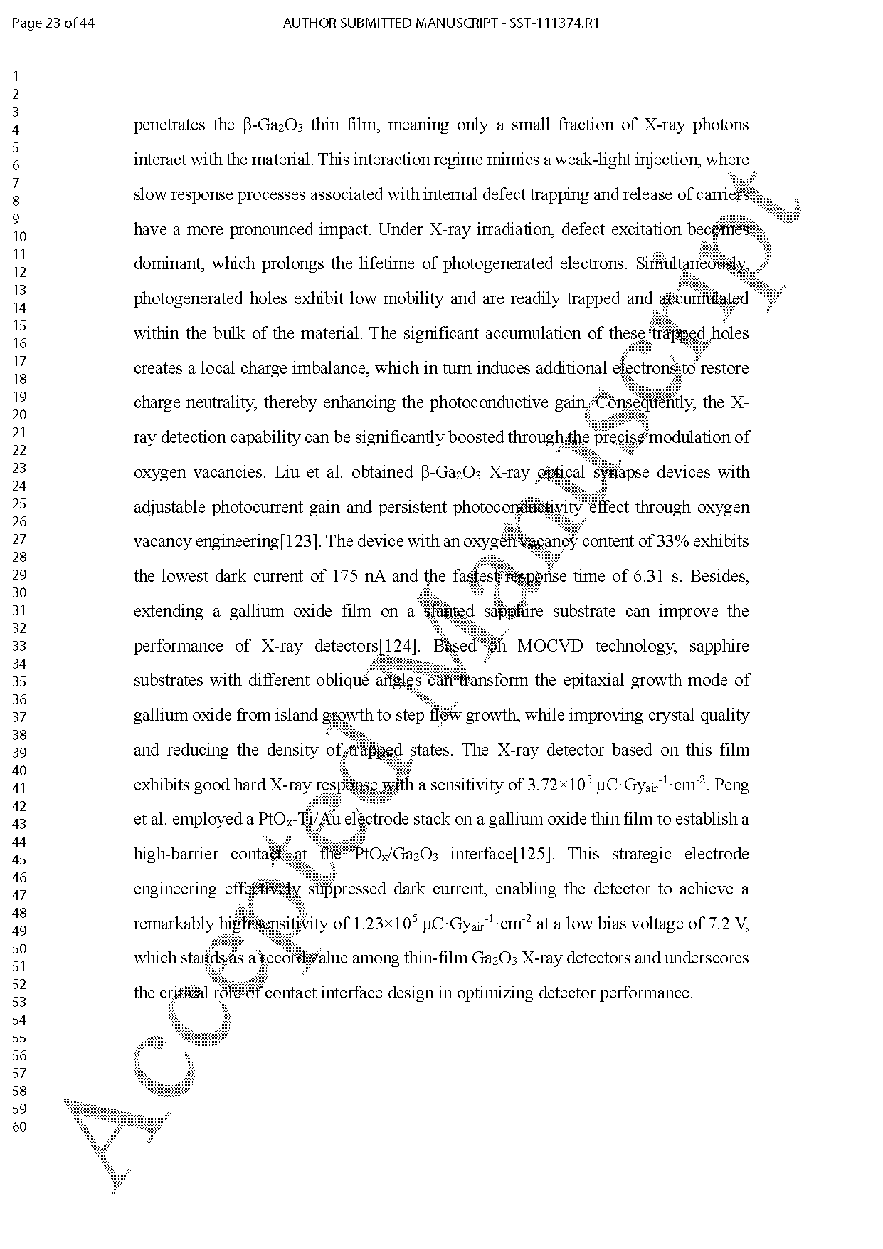
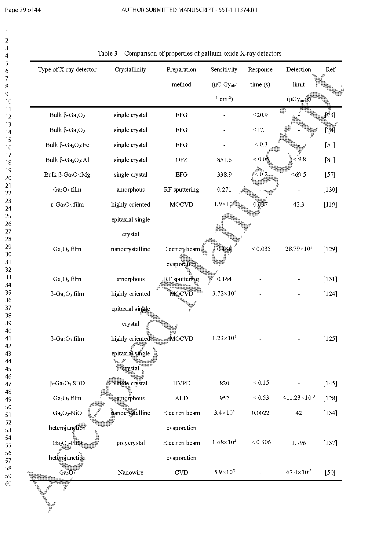
Gallium oxide, as an emerging wide-bandgap semiconductor material, exhibits remarkable properties including a high breakdown electric field, excellent stability, and a strong X-ray absorption coefficient, demonstrating significant potential in the field of X-ray detection. However, Ga₂O₃-based X-ray detectors still face numerous challenges in terms of sensitivity, response time, and large-scale application. At the material level, achieving precise control from bulk single crystals to epitaxial thin films represents a core challenge. Defects such as dislocations and oxygen vacancies act as non-radiative recombination centers, significantly reducing the carrier mobility-lifetime product and directly impairing charge collection efficiency. Particularly in unintentionally doped crystals, shallow donor levels formed by oxygen vacancies lead to excessively high background electron concentrations, severely limiting detector resistivity and dark current performance. Furthermore, the compensation efficiency of acceptor doping (e.g., Fe, Mg) is constrained by dopant solubility, lattice site preference, and their relatively high ionization energy, resulting in only partial ionization at room temperature. Future efforts must focus on systematic defect engineering and doping kinetics studies to establish a correlation model among defect formation energy, doping efficiency, and electrical properties, thereby providing theoretical guidance for producing high-resistivity, low-defect-density Ga₂O₃ materials and fundamentally enhancing detector performance. For devices, the extremely low hole mobility induces space-charge effects, leading to electric field distortion and incomplete charge collection. This not only prolongs carrier transit time but also generates persistent current due to hole trapping, significantly degrading response speed. To overcome this bottleneck, researchers are innovating device structures to implement different photoelectric conversion mechanisms. Examples include constructing heterojunctions to utilize built-in electric fields for directional separation of photogenerated carriers, designing avalanche multiplication structures to achieve carrier number multiplication for substantially improved detection sensitivity, and developing cold-cathode vacuum tube detectors leveraging photoelectric multiplication mechanisms such as electron bombardment-induced photoconductivity (EBIPC). Ga₂O₃ detectors show broad prospects in medical diagnostics and security inspection. Current research has preliminarily demonstrated their potential in X-ray imaging and alarm systems. Ga₂O₃ thin films are particularly suitable for large-area, uniform imaging arrays, where amorphous or polycrystalline films can be integrated with commercial TFT arrays via low-temperature processes, while single-crystal films are suited for high-performance patterned readout systems. However, the limited thickness of thin-film devices (typically only a few hundred nanometers) results in low X-ray attenuation efficiency, restricting absorption efficiency, as a critical trade-off for future applications. Meanwhile, low-dimensional Ga₂O₃ structures such as nanowires offer unique advantages in compact, portable X-ray warning systems due to their high surface-to-volume ratio and distinctive optoelectronic properties. Although research on Ga₂O₃-based X-ray detectors is still in its early stages, continued advancements at the material, device, and application levels will undoubtedly enable them to play an increasingly important role in the future of X-ray detection.
Project Support
This work was supported by the National Key R&D Program of China (No.2022YFB3605400); the National Natural Science Foundation of China (under Grants 62274132).
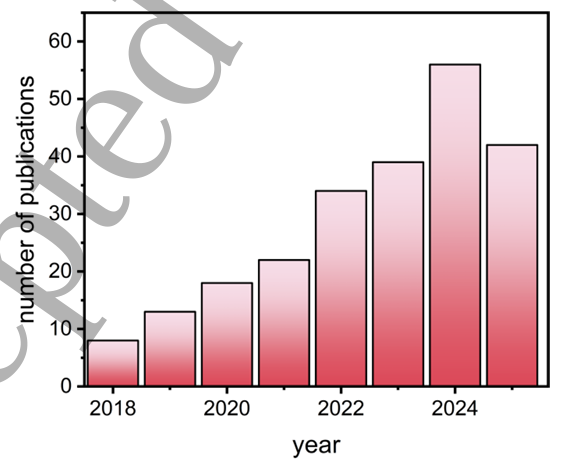
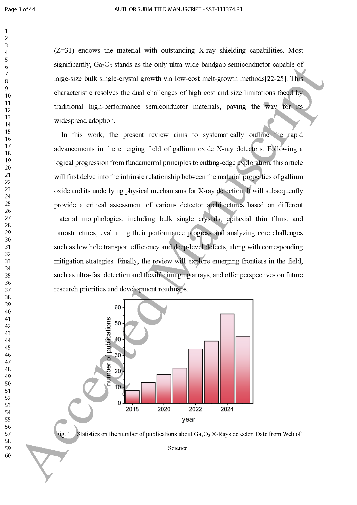
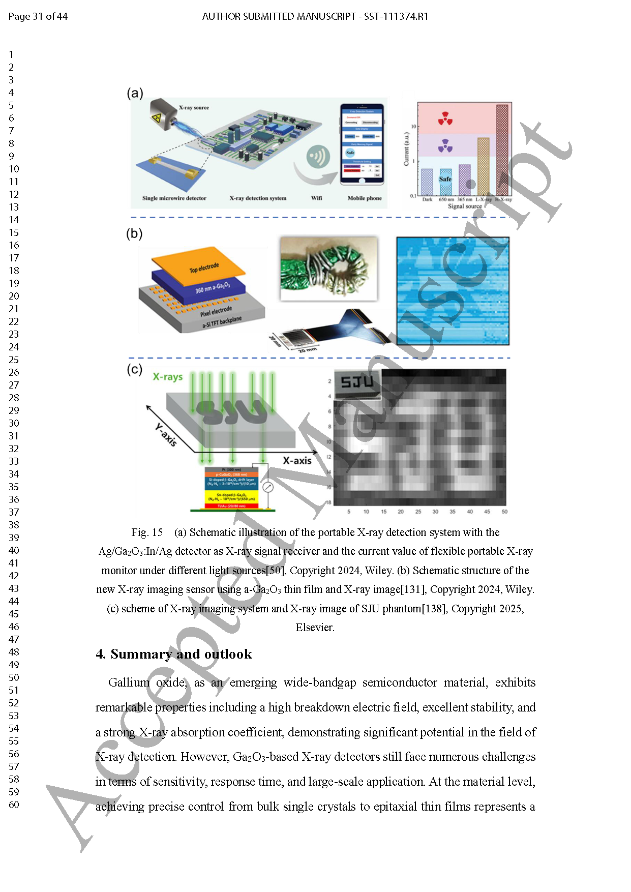
Figure 1 Statistics on the number of publications about Ga₂O₃ X-Rays detector.
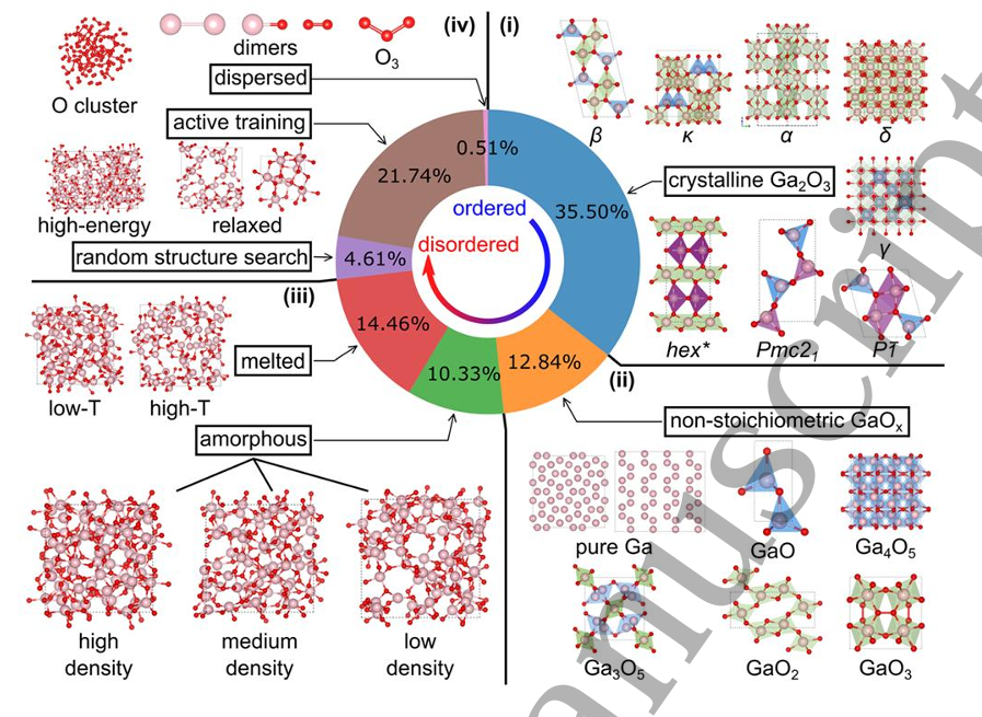
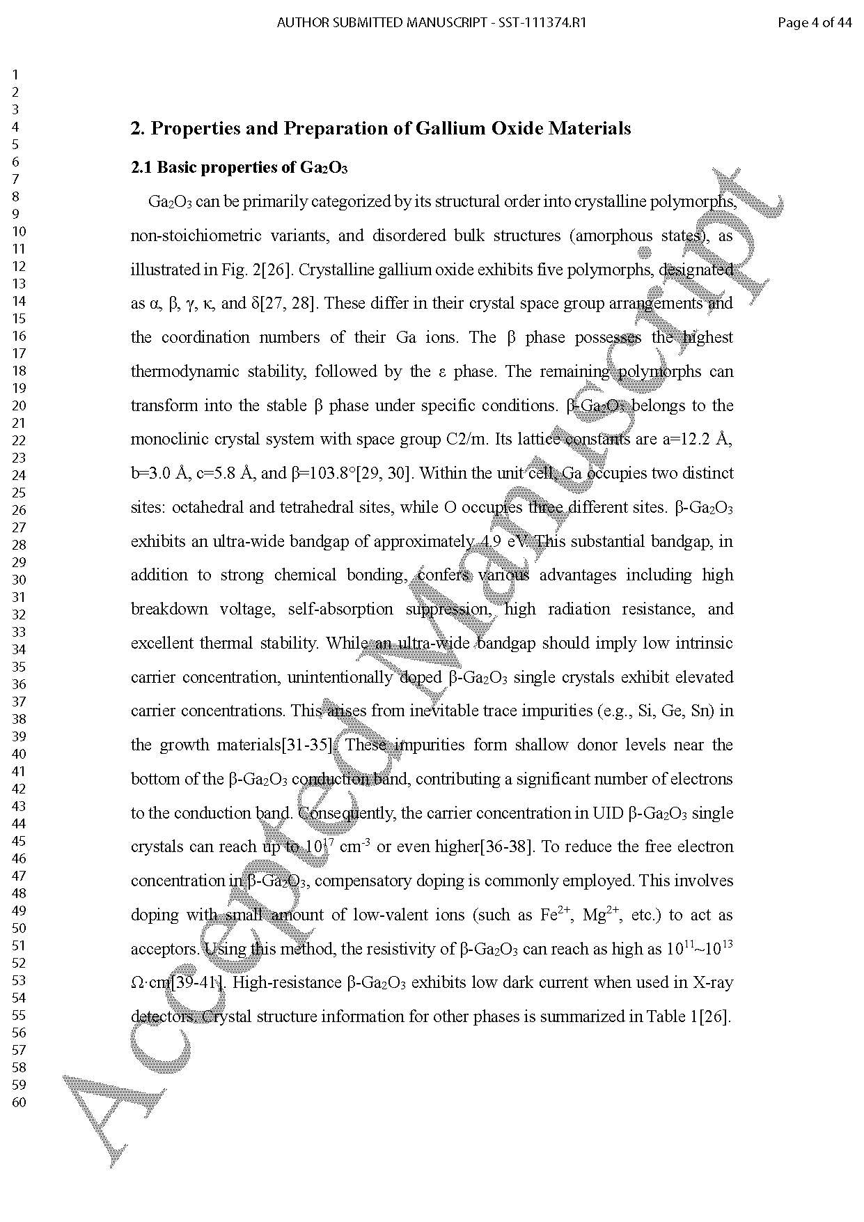
Figure 2 Overview of gallium oxide with different structures.
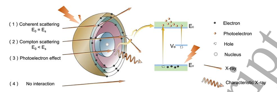
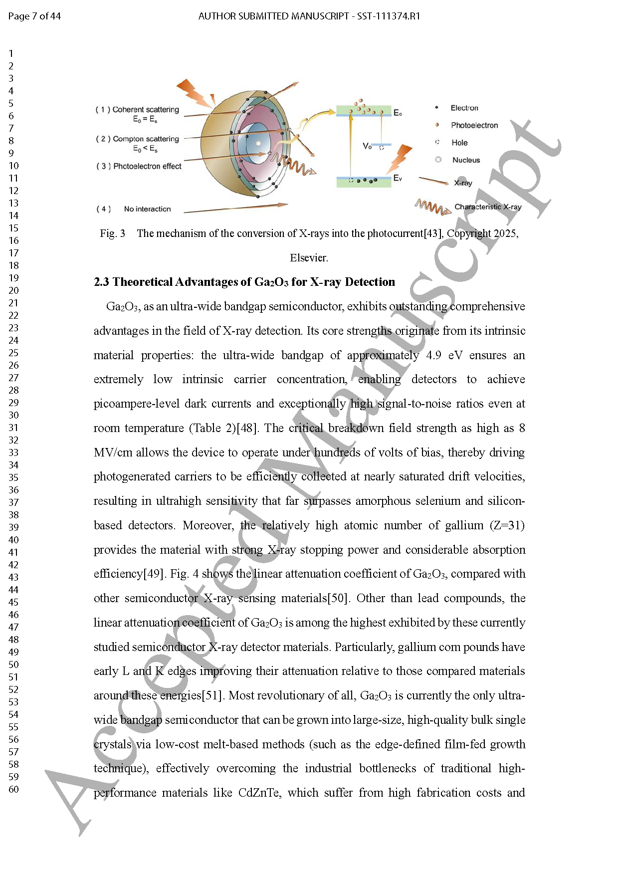
Figure 3 The mechanism of the conversion of X-rays into the photocurrent.
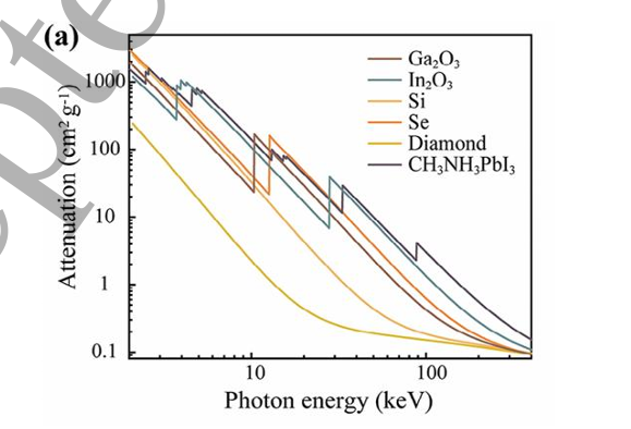
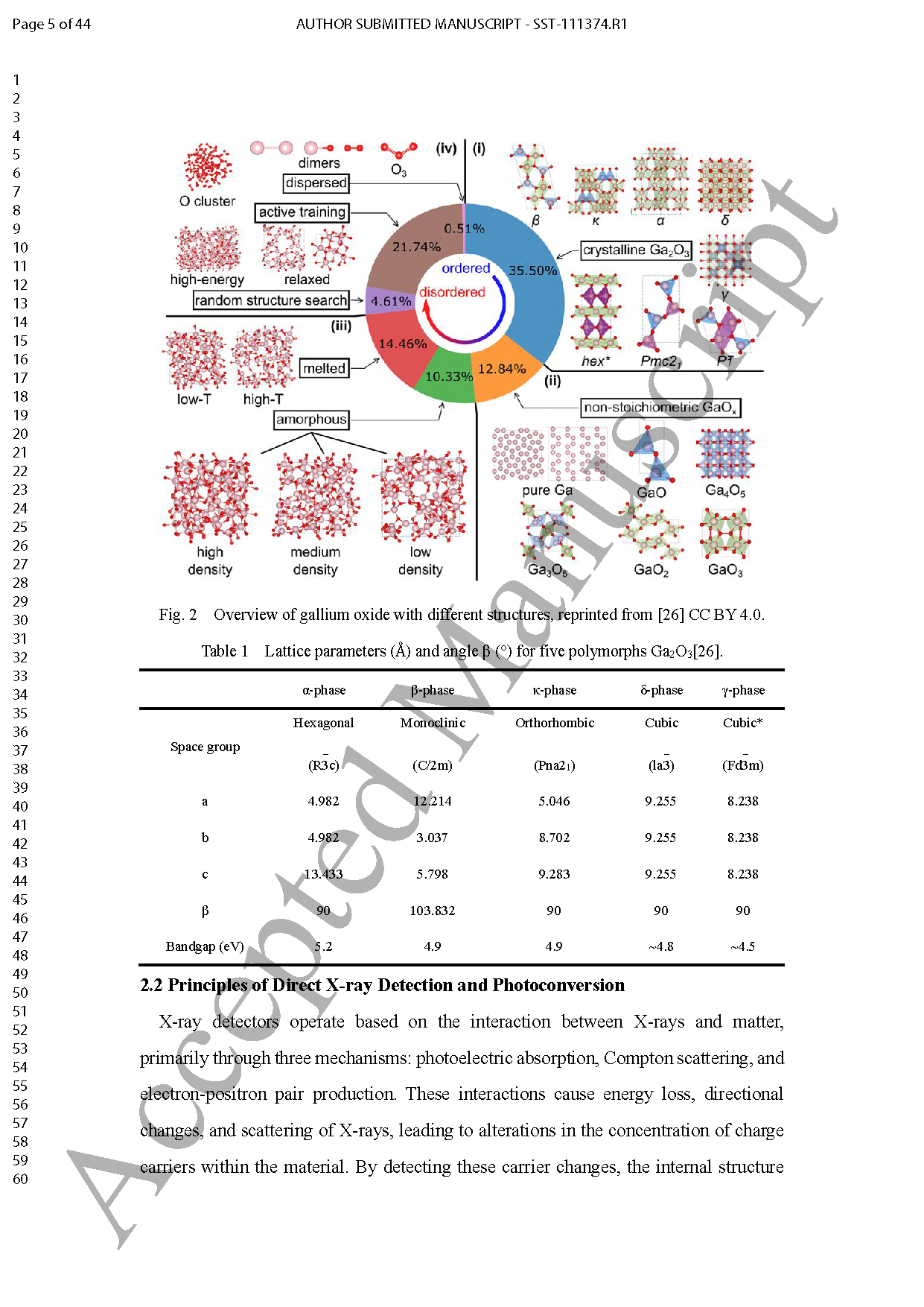
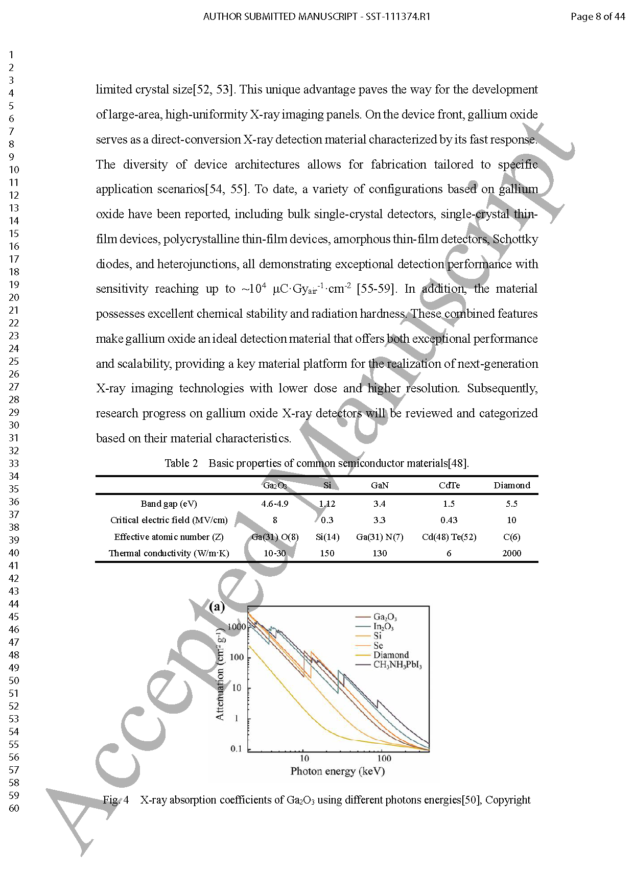
Figure 4 X-ray absorption coefficients of Ga₂O₃ using different photons energies.
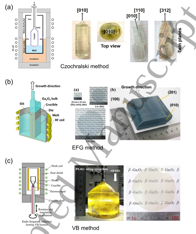
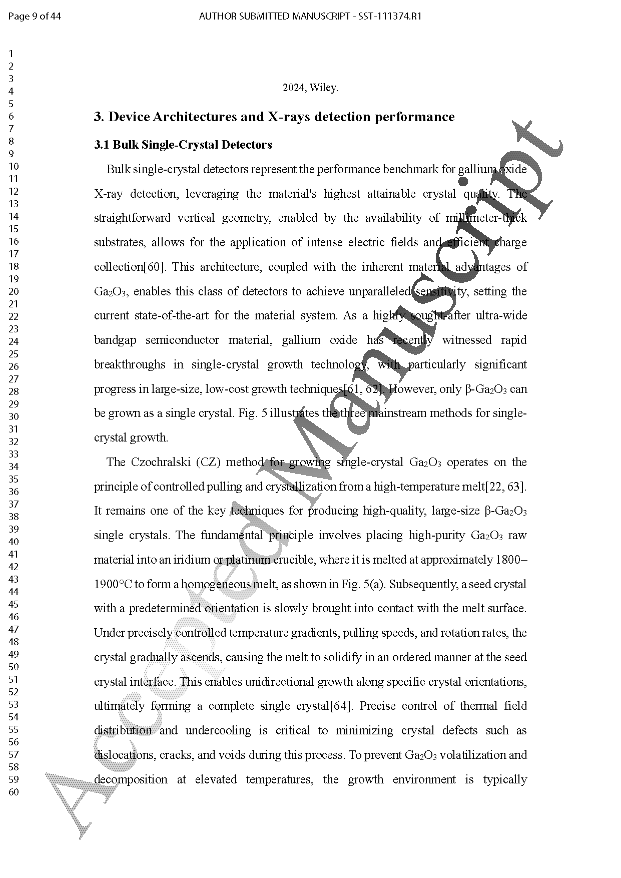
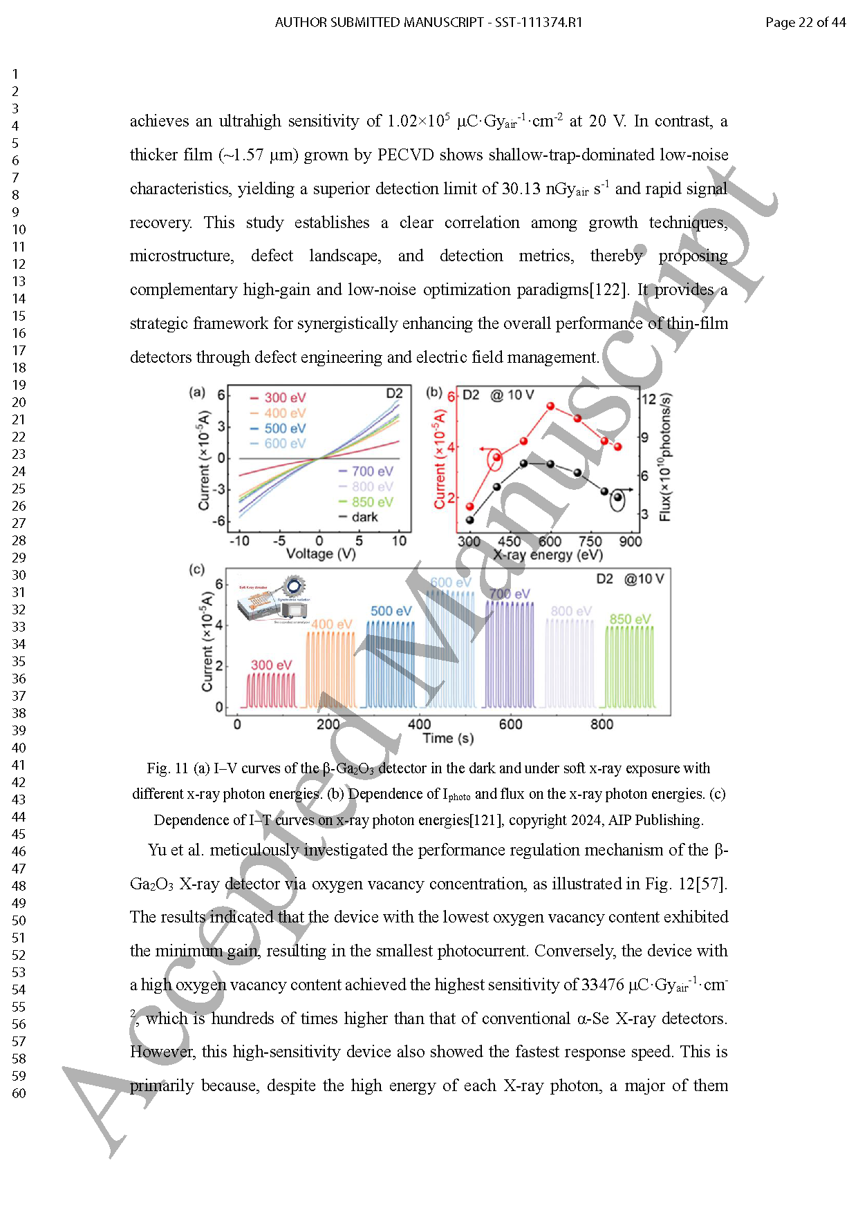
Figure 5 (a) Schematic representation of a Czochralski growth furnace and β-Ga₂O₃ crystals pictures(b) Schematic diagram of the EFG method and Photograph of EFG-grown β-Ga₂O₃ bulk crystal (c) Schematics of Vertical Bridgman furnace and Photographs of 2-inch diameter Fe-doped β-Ga₂O₃ single crystal
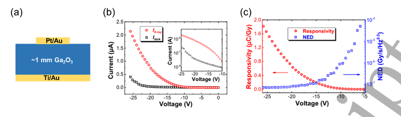
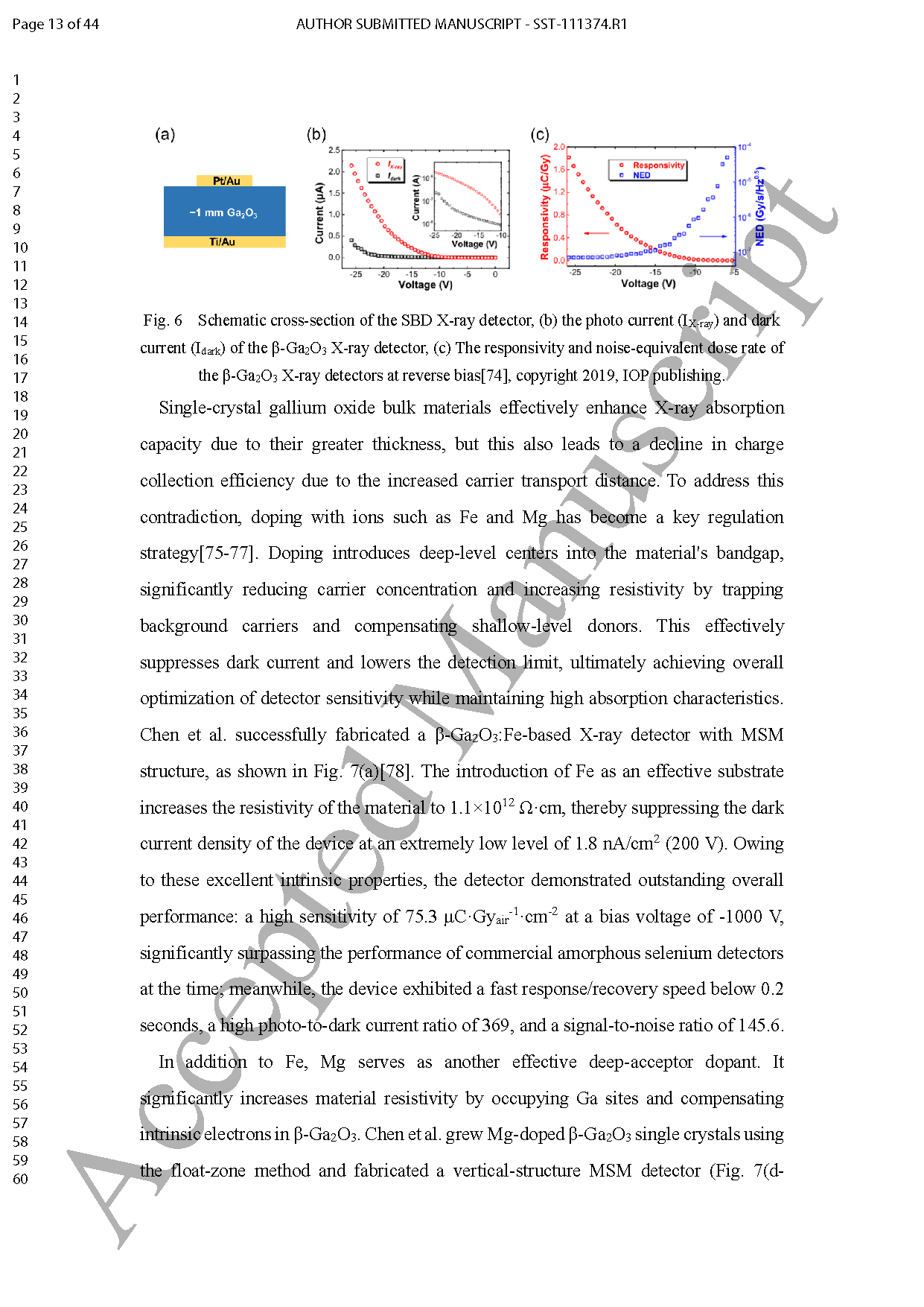
Figure 6 Schematic cross-section of the SBD X-ray detector, (b) the photo current (IX-ray) and dark current (Idark) of the β-Ga₂O₃ X-ray detector, (c) The responsivity and noise-equivalent dose rate of the β-Ga₂O₃ X-ray detectors.
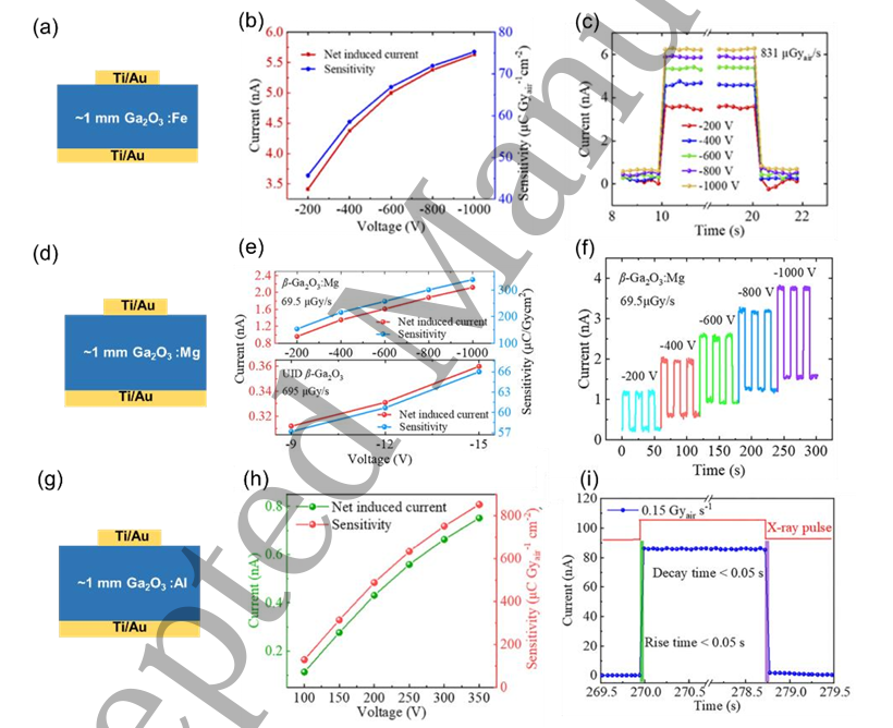
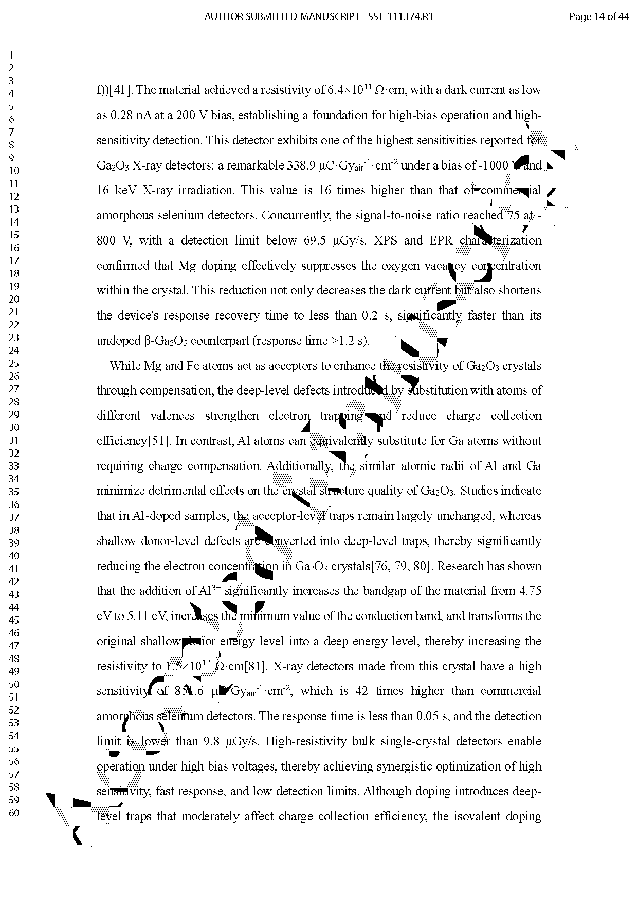
Figure 7 (a) Schematic cross-section of the Ga₂O₃:Fe detector, (b) Both the net induced current and sensitivity of the fabricated Ga₂O₃:Fe detector, (c) Zoom-in time traces of the fabricated detector at different voltages (d) Schematic cross-section of the Ga₂O₃:Mg detector, (e) Net induced current and sensitivity of the detectors at different bias voltages, (f) Transient response of the Ga₂O₃:Mg detectors under X-ray irradiation (g) Schematic cross-section of the Ga₂O₃:Al detector, (h) Net induced current and sensitivity characteristics of Ga₂O₃:Al detector, (i) Response time characteristics of the Ga₂O₃:Al detector measured at 200V.
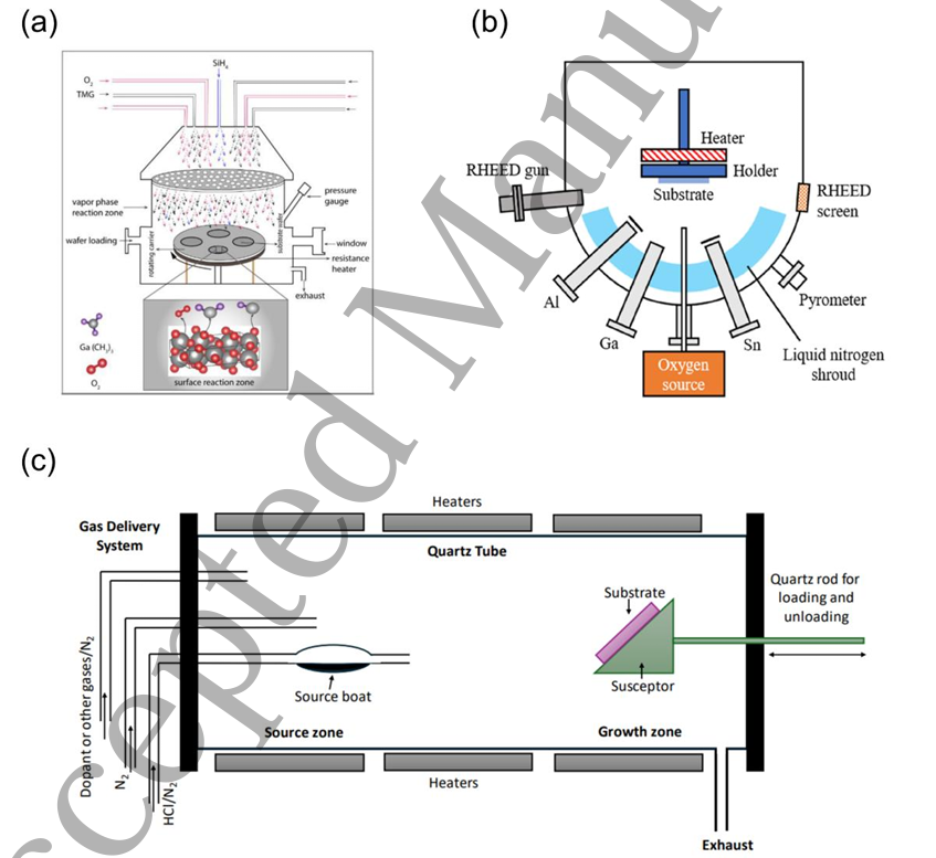
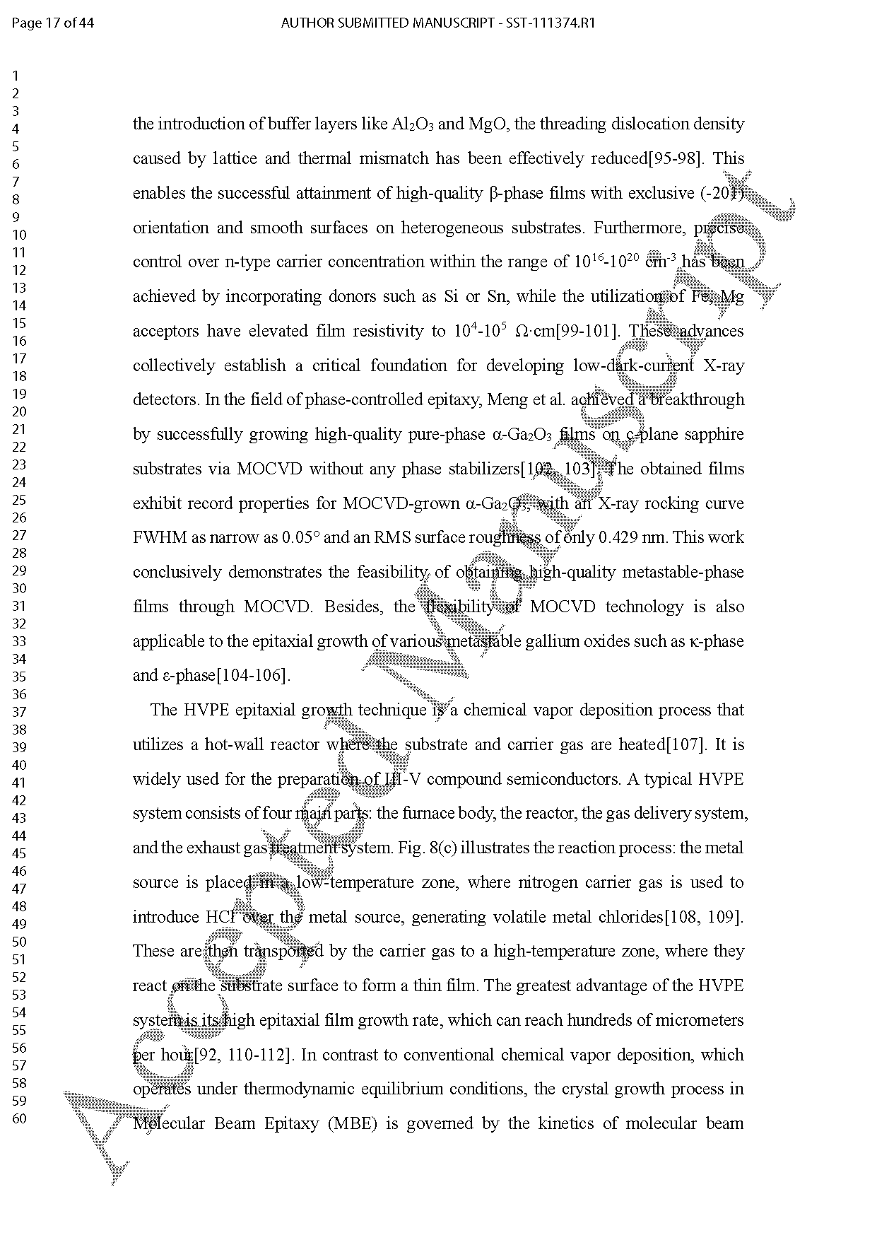
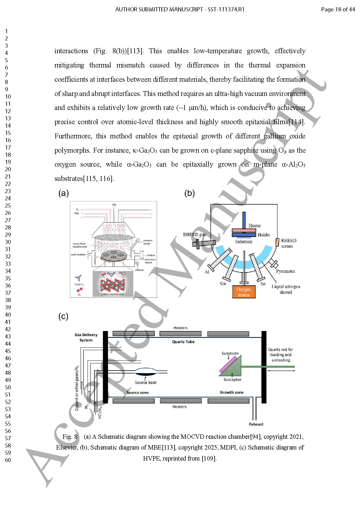
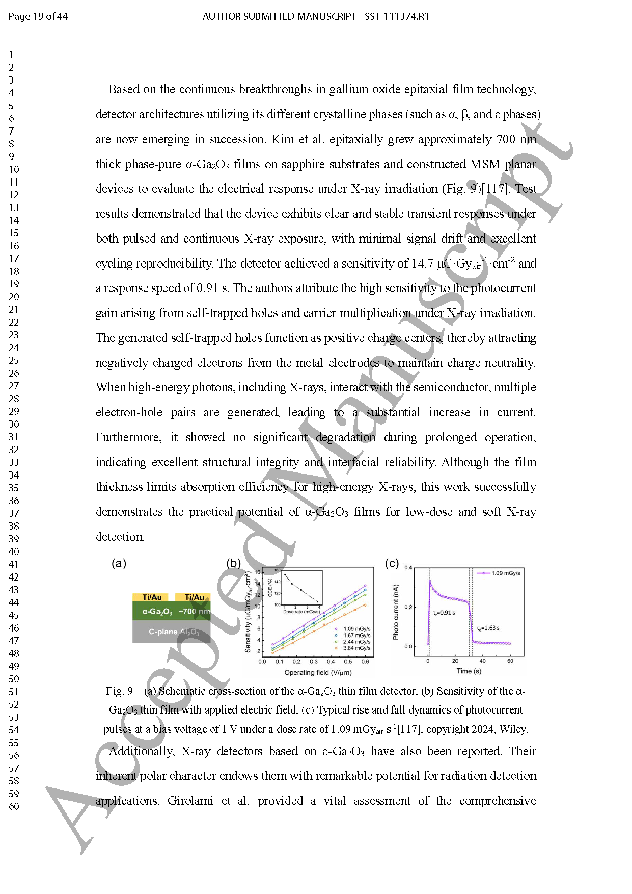
Figure 8 (a) A Schematic diagram showing the MOCVD reaction chamber(b), Schematic diagram of MBE[113], copyright 2025, MDPI, (c) Schematic diagram of HVPE.
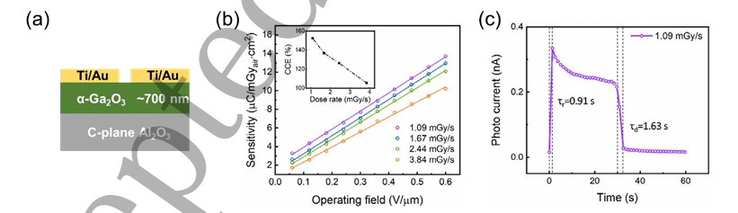
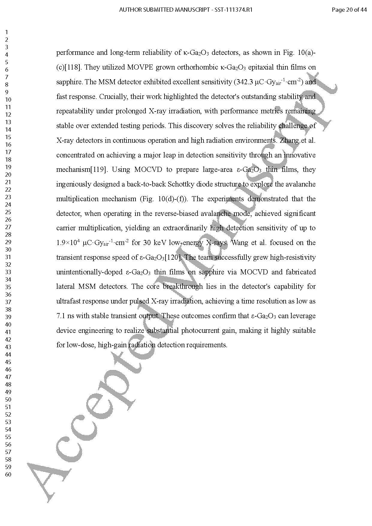
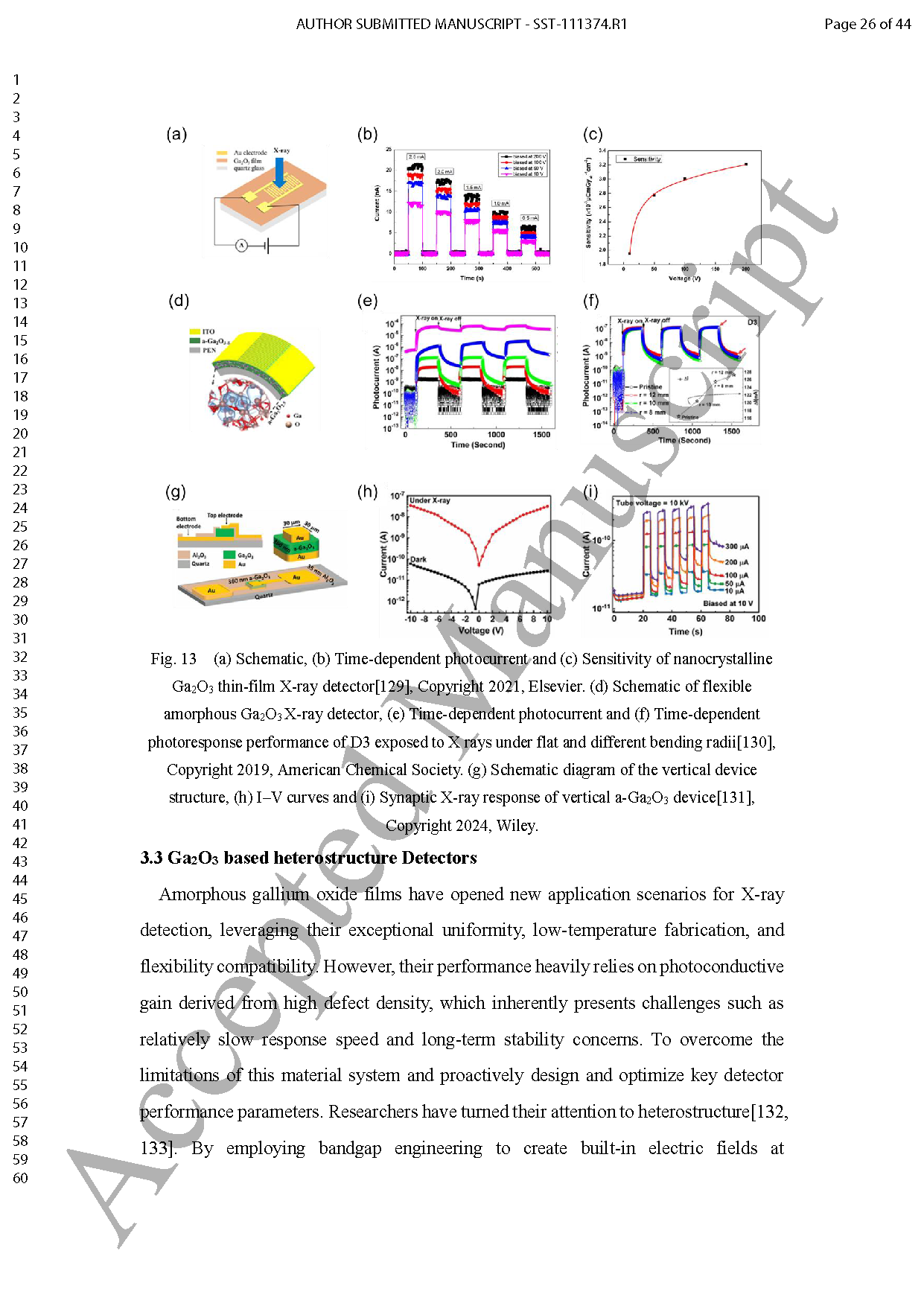
Figure 9 (a) Schematic cross-section of the α-Ga₂O₃ thin film detector, (b) Sensitivity of the α-Ga₂O₃ thin film with applied electric field, (c) Typical rise and fall dynamics of photocurrent pulses at a bias voltage of 1 V under a dose rate of 1.09 mGyair s⁻¹.
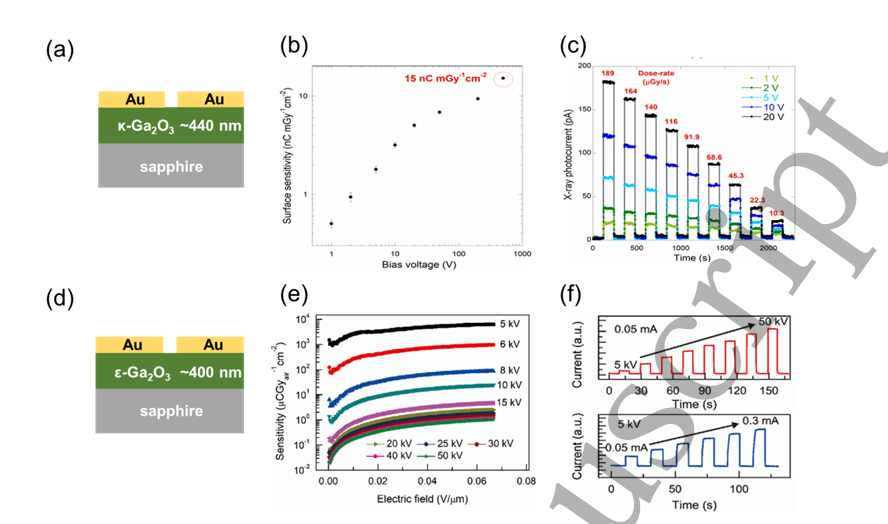
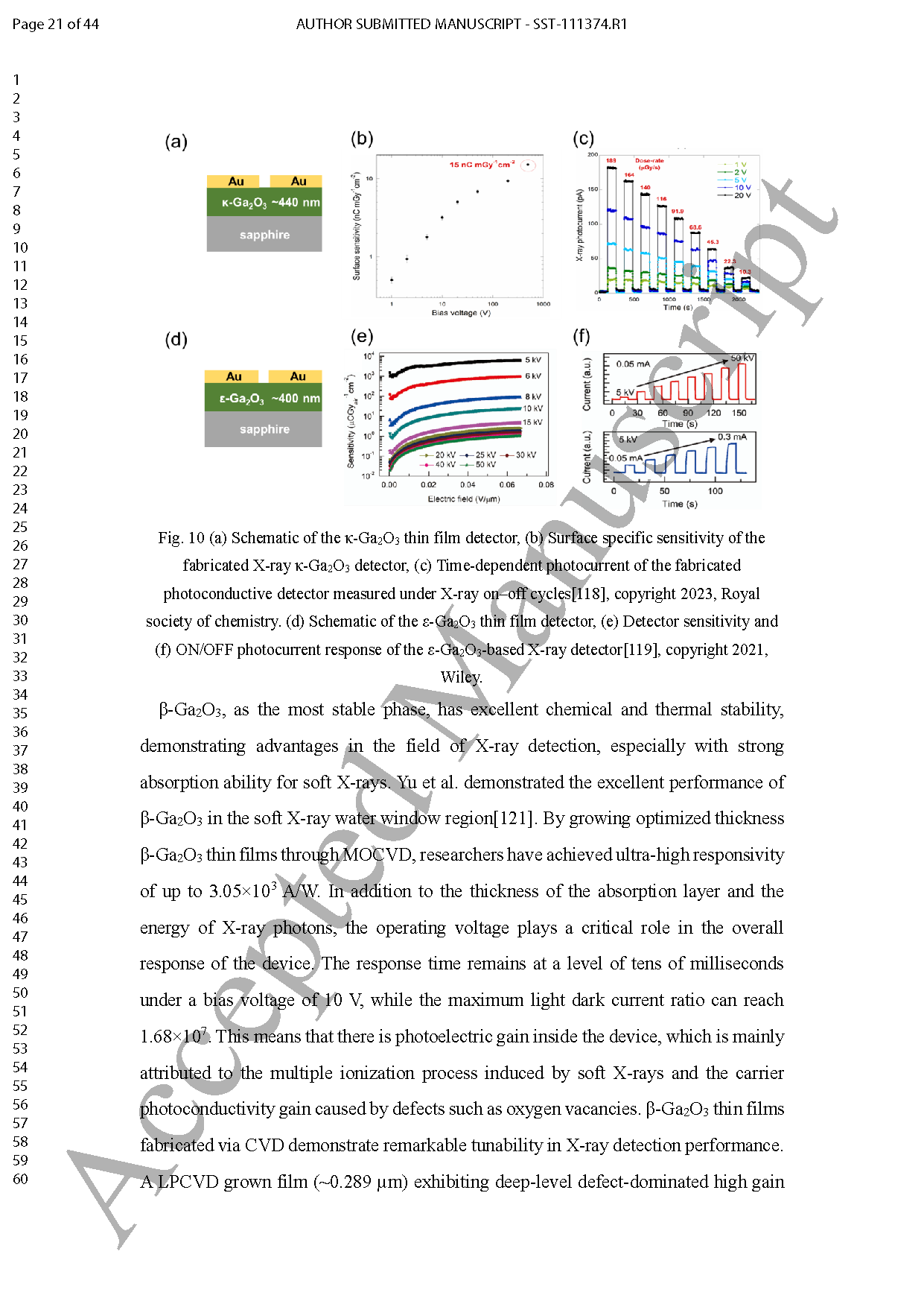
Figure 10 (a) Schematic of the κ-Ga₂O₃ thin film detector, (b) Surface specific sensitivity of the fabricated X-ray κ-Ga₂O₃ detector, (c) Time-dependent photocurrent of the fabricated photoconductive detector measured under X-ray on–off cycles (d) Schematic of the ε-Ga₂O₃ thin film detector, (e) Detector sensitivity and (f) ON/OFF photocurrent response of the ε-Ga₂O₃-based X-ray detector.
DOI:
doi.org/10.1088/1361-6641/ae55bf