


Member News
【Member News】First to Exceed 10 kV! Garen Semiconductor Enables Pinghu Lab to Develop 10 kV-Class Ultra-Low On-Resistance Gallium Oxide Photoconductive Switch
日期:2026-04-07阅读:350
Shenzhen Pinghu Lab, in collaboration with top domestic research teams, has successfully developed a 10 kV-class ultra-low on-resistance Gallium Oxide photoconductive switch. This key device relies on high-quality semi-insulating Gallium Oxide substrates independently developed by Hangzhou Garen Semiconductor and was officially validated and released in February 2026. The achievement breaks the 10 kV barrier, marking China’s global lead in practical 10 kV-class Gallium Oxide devices and securing a leading position in fourth-generation ultra-wide bandgap semiconductor materials and devices.
High-Quality Material Ensures Excellent Devices
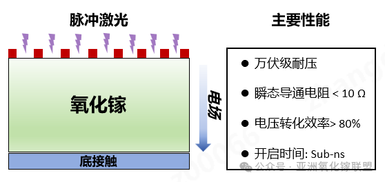
The switch achieves breakdown voltage > 10,000 V, ultra-low on-resistance (<10 Ω), sub-nanosecond (<1 ns) response, high stability, and other outstanding performance, reaching international leading levels. Compared with traditional industry standards, it greatly enhances voltage capability while reducing conduction loss, applicable in high-voltage DC intelligent control, high-power pulse generation, advanced accelerators, and defense high-tech equipment, solving the long-standing bottleneck of high-voltage, ultra-fast, low-resistance devices.
Garen Semiconductor’s 8-inch Gallium Oxide substrates play a decisive role, offering excellent crystal quality, high thickness uniformity, and stable electrical properties. They meet stringent requirements for large, low-defect, highly consistent high-voltage devices and support engineering validation of 10 kV-class devices, laying a solid foundation for large-power, high-voltage Gallium Oxide devices.
Leading the Full Technology Chain
Garen Semiconductor continues to advance the Gallium Oxide field and achieved the world’s first 8-inch Gallium Oxide homoepitaxial growth in March 2026, effectively breaking a key bottleneck in Gallium Oxide industrialization and reshaping the global competitive landscape. In addition, the company has developed the “SCIENCE Series” research-grade VB crystal growth systems tailored for Gallium Oxide research, leveraging fully proprietary core technologies to enable efficient scientific exploration.
The company has established large-scale manufacturing capabilities for Gallium Oxide substrates across multiple sizes, with substrate flatness, dislocation density, and electrical properties all reaching world-leading levels. It also possesses mature Gallium Oxide homoepitaxy processes, enabling the stable production of high-voltage, low-loss, high-power epitaxial wafers. Its product portfolio comprehensively supports devices including photoconductive switches, MOSFETs, diodes, and detectors.
Currently, Garen Semiconductor has achieved stable supply of 8-inch Gallium Oxide homoepitaxial wafers, with multiple key metrics reaching internationally advanced levels, fully supporting universities, research institutes, and device companies in cutting-edge research across high-voltage, high-frequency, high-power, and optoelectronic applications.
Intelligent Core Equipment Supports Advanced Research
The “SCIENCE Series” ensures stability, precision, and compatibility. It flexibly supports different single-crystal sizes without frequent component changes, achieves ±0.1 °C temperature control accuracy with automated composite measurement and control, and provides visual interfaces and intelligent data recording for real-time monitoring and reduced errors.
The “SCIENCE Series” is now fully available. Garen Semiconductor remains committed to open collaboration and co-innovation, partnering with global labs, chip designers, and system manufacturers to empower top-tier devices with first-class materials, drive the industrial ecosystem, and promote Gallium Oxide from research breakthroughs to large-scale industrialization.
About GAREN SEMI
Hangzhou Garen Semiconductor Co., Ltd. is a world-leading provider of Gallium Oxide materials and equipment solutions, focusing on R&D and industrialization in the ultra-wide bandgap semiconductor field. The company’s core products include 2–8-inch Gallium Oxide single crystals and substrates (with 8-inch being the world’s first), Gallium Oxide Vertical Bridgman (VB) crystal growth equipment, Gallium Oxide epitaxial wafers, etc. It is committed to building a full-chain product system of “equipment–crystal–substrate–epitaxy” to provide systematic solutions for global customers. The company’s achievements in Gallium Oxide have been specially reported by well-known media including People’s Daily, Xinhua News Agency, Science and Technology Daily, Sina Finance, China Blue News, and The Paper.
Enterprise Honors Summary
Recognized as a National-level Science and Technology Small and Medium-sized Enterprise and Zhejiang Innovative Small and Medium-sized Enterprise in 2023;Awarded Zhejiang Specialized, Sophisticated, Unique and New Small and Medium-sized Enterprise in 2024;Approved as a High-tech Enterprise in 2025;Won the SEMI Outstanding Contribution Award for Sustainable Development at SEMICON CHINA 2025, the Together Progress Award at the Jufeng Summit Forum (JFSC) and Compound Semiconductor Industry Expo, the Innovation Vitality Award of Zhejiang Semiconductor Industry, the Second Prize in the Enterprise Group of the 10th “Maker China” Zhejiang Provincial Finals, the Top 500 Enterprise Group of the 10th “Maker China” SME Innovation and Entrepreneurship Competition, and the 2024–2025 Semiconductor Material Industry Contribution Award;The major breakthrough in the preparation of 8-inch Gallium Oxide single crystals and substrates was selected as one of the “Top 10 Advances in China’s Third-Generation Semiconductor Technology 2025” and “Major Scientific and Technological Achievements 2025” by the Department of Science and Technology of Zhejiang Province;Led the formulation of 2 group standard drafts, participated in drafting 1 national standard, and participated in promoting 1 group standard draft in the Gallium Oxide field;Supported by the “5213” Excellence Program of Xiaoshan District, Hangzhou, Zhejiang Province, and approved to establish Zhejiang Enterprise Research Institute;Obtained the quality management system certification;Granted 14 authorized invention patents at home and abroad (including patents in the US, Japan and other countries), with more than 50 patents pending.
For more information about Garen Semiconductor and its products, please visit our official website: http://garen.cc/
Or contact us via the following ways:
Mr. Jiang: 15918719807
E-mail: jiangjiwei@garen.cc
Mr. Xia: 19011278792
E-mail: xianing@garen.cc
