Paper Sharing
【Domestic Papers】All-Optical Artificial Synapse Based on ε-Ga₂O₃ and β-Ga₂O₃ Mixed-Phase Thin Films
日期:2026-04-08阅读:281
Researchers from the North China Electric Power University have published a dissertation titled " All-Optical Artificial Synapse Based on ε-Ga2O3 and β-Ga2O3 Mixed-Phase Thin Films " in Materials
Background
With the advent of the era of artificial intelligence and big data, the traditional von Neumann computing architecture faces increasingly prominent challenges due to the separation of storage and computation and high energy consumption. Neuromorphic computing offers a revolutionary pathway to achieving energy-efficient, parallelized novel computing paradigms by simulating the dynamic plasticity of neurons and synapses. Among these, artificial synapses serve as the fundamental building blocks of neural networks, with their performance directly determining the functionality and complexity of neuromorphic systems. In recent years, a wide variety of neuromorphic devices primarily relying on electrical stimulation have emerged in large numbers. Although these artificial synapses provide a promising hardware foundation for the development of neuromorphic computing chips, inherent issues such as electrical crosstalk limit their operational speed and response bandwidth. Significant progress has been made in developing artificial synapses based on structures such as memristors, floating-gate transistors, and photoconductive devices. Among these, oxide semiconductors (e.g., ZnO, TiO2) have been extensively studied due to their ion migration and oxygen vacancy regulation mechanisms. However, existing devices mostly rely on electrical stimulation to update synaptic weights, which leads to issues such as electrical crosstalk and high energy consumption. Optical synapse devices utilize light as the stimulus source instead of electrical pulses, enabling neuromorphic systems with high-speed transmission, high bandwidth, low crosstalk, and greater energy efficiency. This represents a crucial direction for overcoming the limitations of electrical synapses, demonstrating unique advantages particularly in all-optical neuromorphic systems
Abstract
All-optical memristors possess light-sensing and storage capabilities while simultaneously simulating human synaptic functions, demonstrating immense potential in the field of brain-inspired computing for realizing bionic synapses and brain-like intelligence. In this work, we successfully produced ε-Ga2O3 films, ε/β-Ga2O3 mixed-phase films, and β-Ga2O3 films via chemical vapor deposition (CVD). The optical output and optical response characteristics of the thin films are investigated under 254 nm and 365 nm lasers. The CVD-grown ε-Ga2O3 is found to process a small amount of defects and insignificant memristive properties and the β-Ga2O3 obtained from the annealing of ε-Ga2O3 exhibits superior crystal quality but lacks memristive properties, while the ε/β-Ga2O3 mixed-phase films grown directly by CVD contain a fair amount of defects and demonstrate persistent resistance retention exceeding 104 s. Based on the excellent memristive properties of ε/β-Ga2O3 mixed-phase films, we conducted experiments simulating optical synapses. By adjusting optical pulse parameters (intensity, repetition rate, and duration), we successfully modeled the short-term plasticity (STP) and long-term plasticity (LTP) observed in biological synapses. Experiments confirm that light stimulation can effectively induce synaptic behaviors, such as the progressive conversion of short-term memory (STM) into long-term memory (LTM), and further fully reproduce the neuroplasticity process of “learning-forgetting-relearning.” This study demonstrates a photoconductive synapse memristor based on the wide-bandgap material gallium oxide, exhibiting exceptional air stability with sustained photoconductivity maintained for over a year. This study provides new insights into the practical application feasibility of all-optical artificial synapses based on gallium oxide.
Conclusion
This study demonstrates a photoresistive memristor based on the wide-bandgap material gallium oxide, integrating functions such as optical synapses and data storage. CVD technology has been successfully applied to deposit epsilon-Ga2O3 and beta-Ga2O3 films on sapphire (0001) substrates. This study further utilized CVD technology to fabricate beta/epsilon mixed-phase Ga2O3 films. By comparing three distinct gallium oxide films, it was discovered that the film exhibiting both beta and epsilon crystalline phases demonstrates significant absorption under deep ultraviolet light at 254 nm wavelength. It also exhibits solar-blind sensitivity characteristics. Compared to pure epsilon-phase and beta-phase gallium oxide, it exhibits more pronounced memristive properties. Further testing demonstrates that the MSM structure fabricated from this film exhibits outstanding optoelectronic synaptic functionality as a synapse device and memory unit, including STP, LTP, and “learning-forgetting-relearning” processes. Benefiting from the synergistic properties of two gallium oxide crystal phases, the device exhibits outstanding non-volatility. Notably, its resistive state retention time exceeds 104 s, coupled with long-term stability on an annual scale (>1 year). This achievement lays a crucial foundation for developing advanced neuromorphic systems that simulate long-term memory and sustained learning. Looking ahead, the introduction of paired spike-timing-dependent plasticity (STDP)-like learning rules in such devices, thereby further simulating the temporal plasticity observed in biological synapses. Based on the photonic–electrical synergistic properties of gallium oxide, the all-optical artificial synapse demonstrated significant potential in the field of neuromorphic computing.
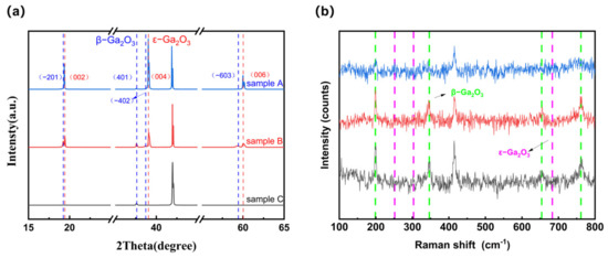
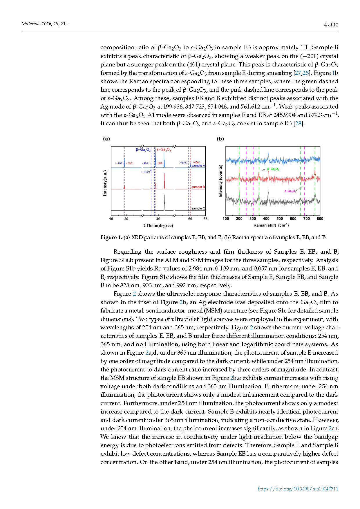
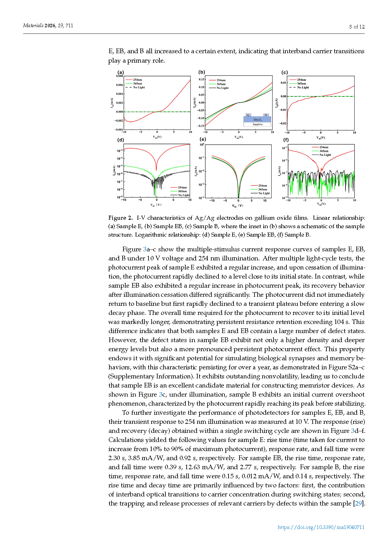
图1. (a) 样品 E、EB 和 B 的 X 射线衍射(XRD)图谱;(b) 样品 E、EB 和 B 的拉曼光谱图。
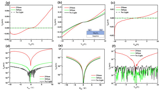
图2: 氧化镓薄膜上 Ag/Ag 电极的 I - V 特性。线性关系:(a)样品 E,(b)样品 EB,(c)样品 B,其中(b)中的插图显示了样品结构的示意图。对数关系:(d)样品 E,(e)样品 EB,(f)样品 B。
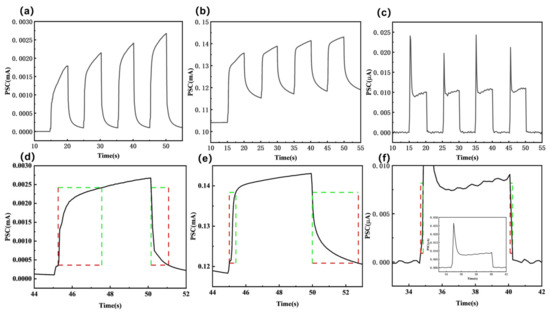
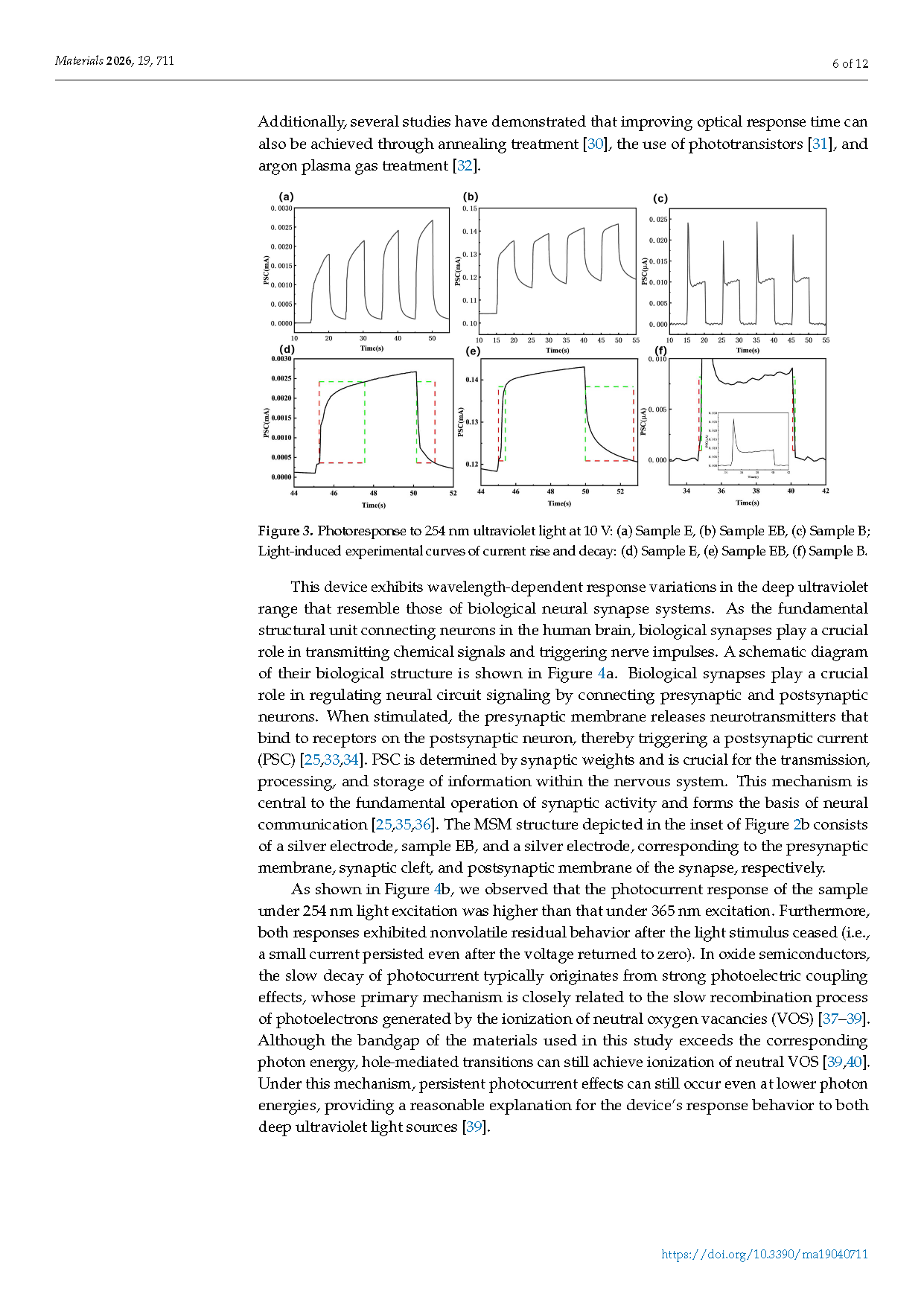
图3. 在 10 V 电压下对 254 nm 紫外光的光响应:(a)样品 E(b)样品 EB(c)样品 B;光诱导电流上升和衰减的实验曲线:(d)样品 E,(e)样品 EB,(f)样品 B。
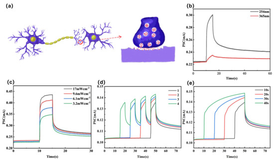
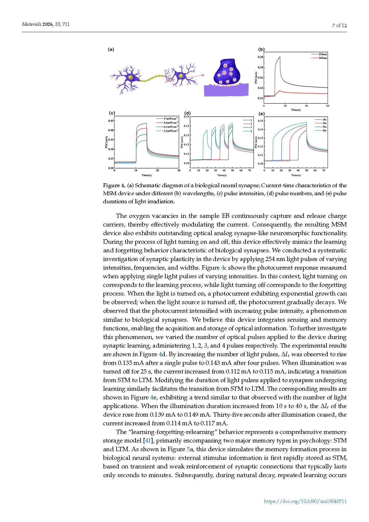
图4. (a) 生物神经突触示意图;MSM 器件在不同(b)波长(c)脉冲强度(d)脉冲次数和(e)光照射脉冲持续时间下的电流-时间特性。
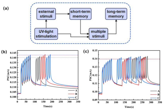
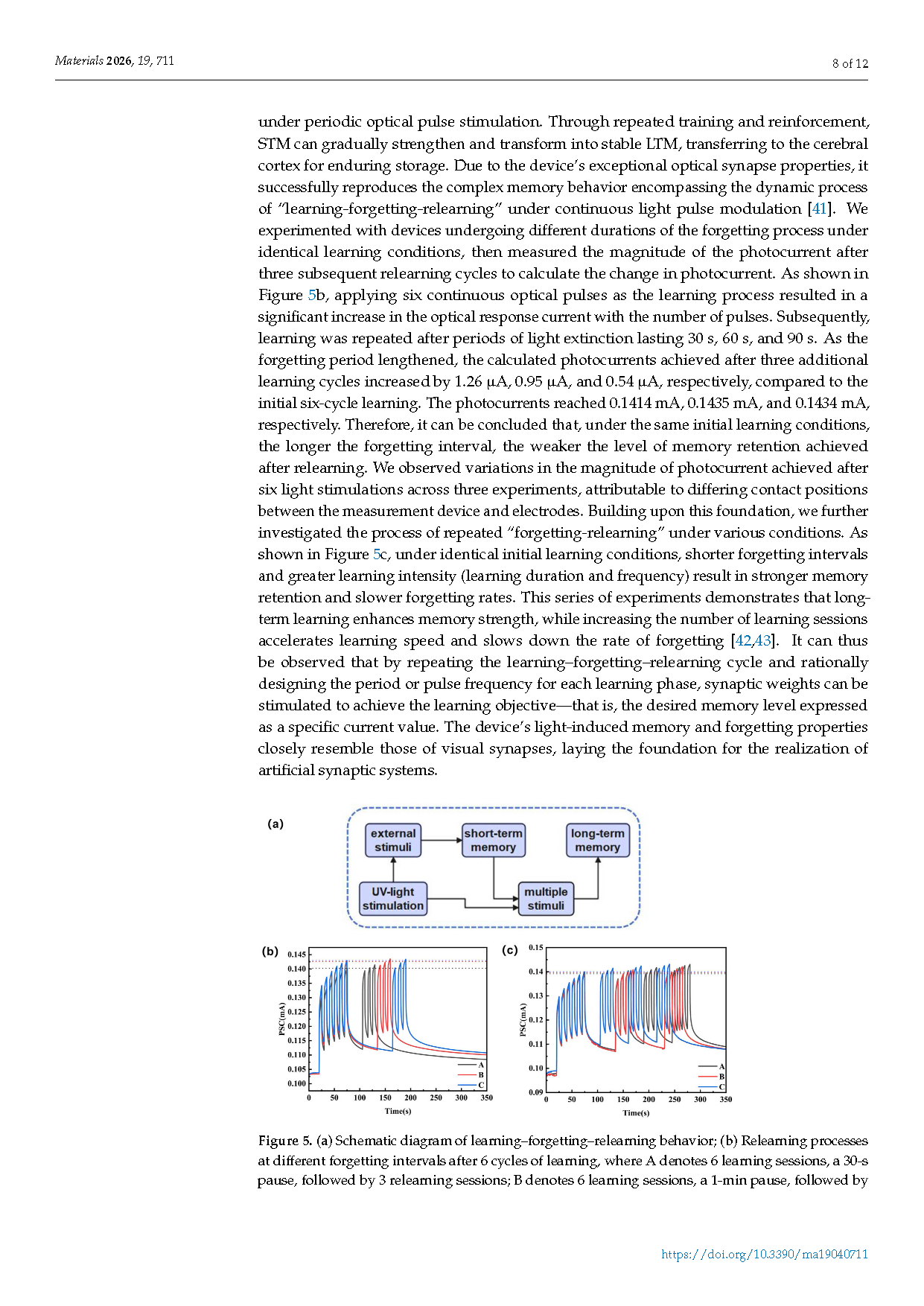
图5. (a) 学习-遗忘-再学习行为示意图;(b) 6个学习周期后不同遗忘间隔的再学习过程,其中 A 表示 6 次学习后暂停 30 秒,接着进行 3 次再学习;B表示 6 次学习后暂停 1 分钟,接着进行 3 次再学习;C 表示 6 次学习后暂停 1 分钟 30 秒,接着进行 3 次再学习;(c) 6 个学习周期后的不同“遗忘-再学习”模式:A 表示 6 次学习后遗忘 1 分钟,接着进行 3 轮再学习,每轮间隔 30 秒;B 表示 6 次学习后遗忘 1 分钟,接着进行 2 轮再学习,每轮间隔 1 分钟;C 表示 6 次学习后遗忘 30 秒,接着进行 3 轮再学习,每轮间隔 30 秒。
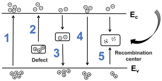
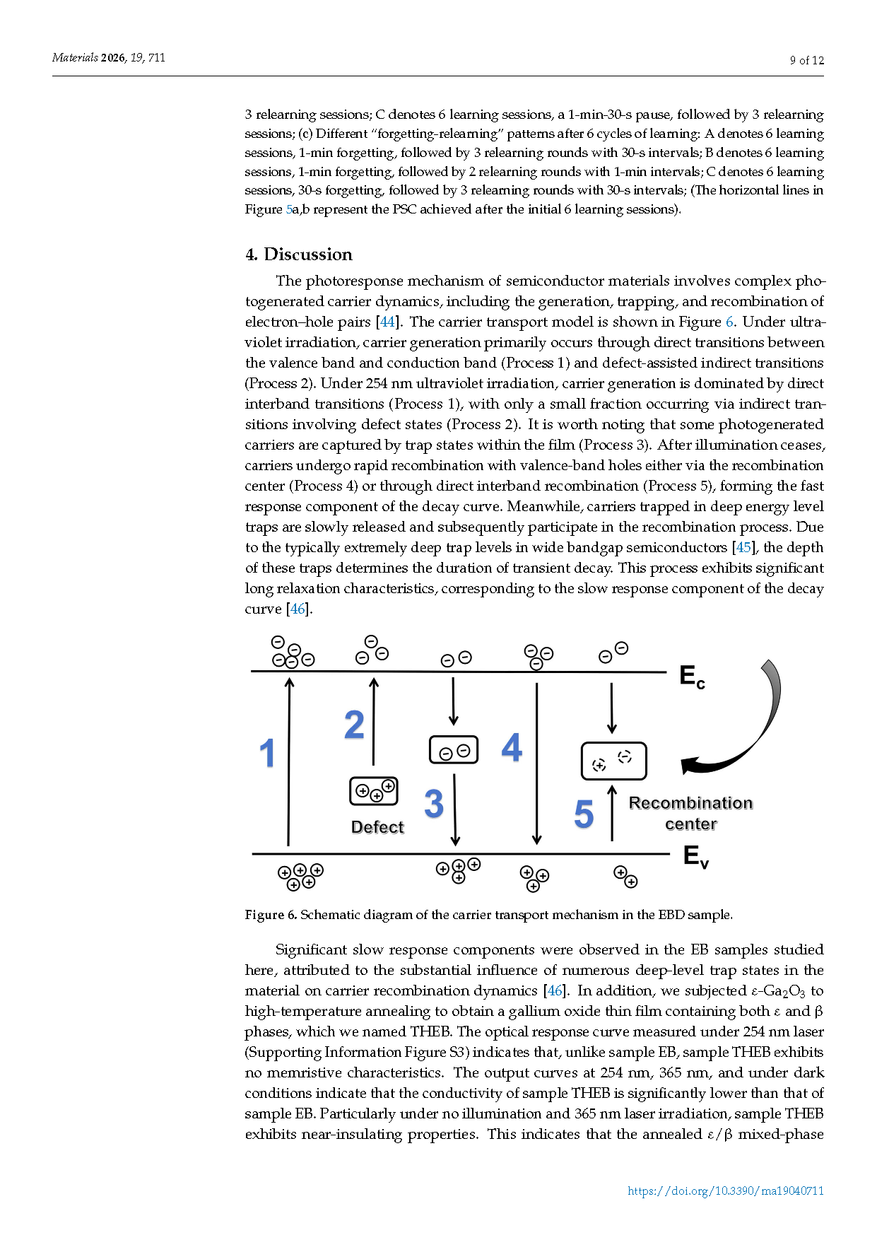
图6. EBD 样品中载流子传输机制的示意图。
DOI:
doi.org/10.3390/ma19040711