Paper Sharing
【International Papers】Synaptic κ-Ga₂O₃ Photodetectors for Privacy-Enhancing Neuromorphic Computing
日期:2026-04-09阅读:236
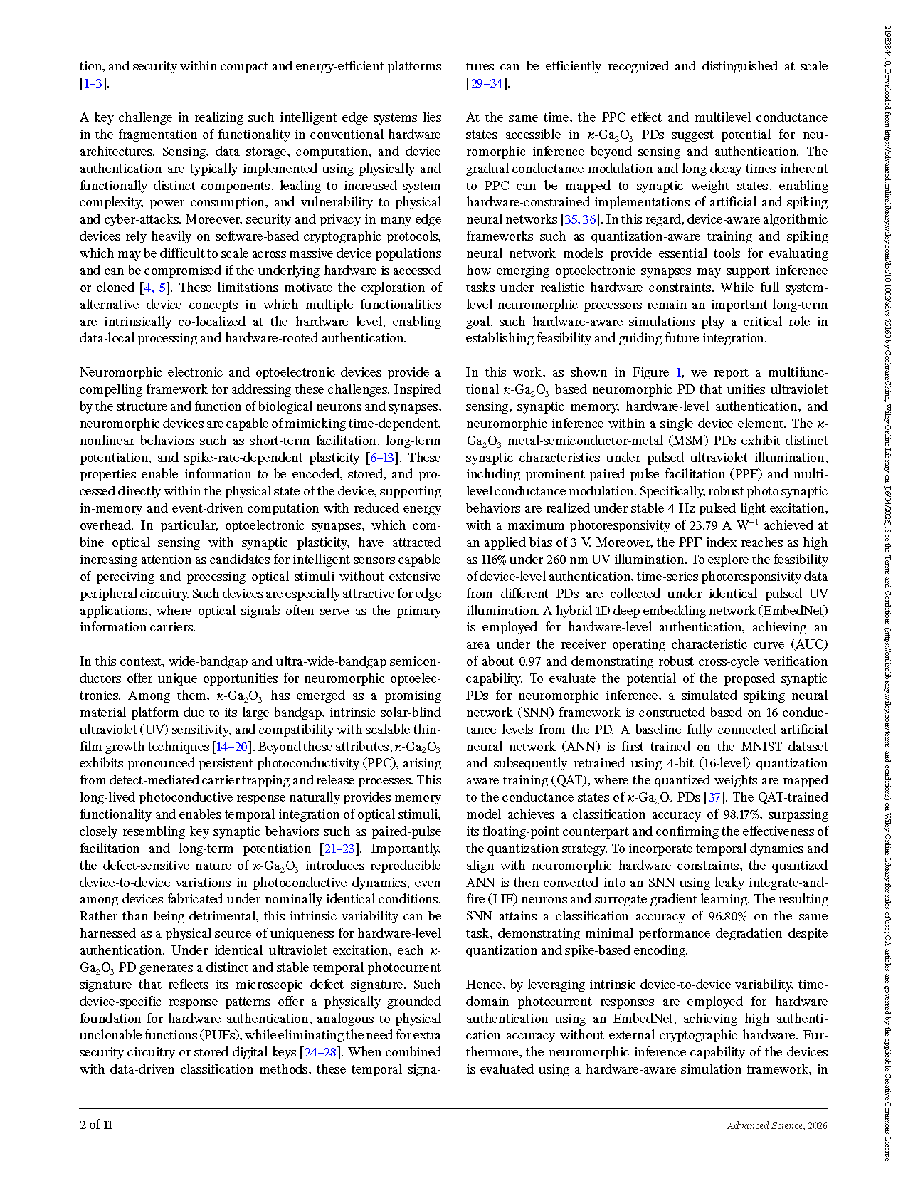
Researchers from the King Abdullah University of Science and Technology (KAUST) have published a dissertation titled "Synaptic κ-Ga₂O₃ Photodetectors for Privacy-Enhancing Neuromorphic Computing" in Advanced Science.
Background
The rapid proliferation of the Internet of Things (IoT) is driving the deployment of vast numbers of distributed sensing nodes across application domains ranging from smart infrastructure and industrial automation to environmental monitoring and healthcare. As the volume and dimensionality of data generated at the network edge continue to increase, conventional cloud-centric computing architectures face growing challenges related to latency, energy consumption, and data privacy. In response, edge computing has emerged as a critical paradigm that seeks to process and interpret data as close as possible to the point of acquisition, thereby reducing communication overhead while enabling faster, more context-aware responses. This shift places new and stringent demands on edge hardware, which must increasingly integrate sensing, memory, computation, and security within compact and energy-efficient platforms.
A key challenge in realizing such intelligent edge systems lies in the fragmentation of functionality in conventional hardware architectures. Sensing, data storage, computation, and device authentication are typically implemented using physically and functionally distinct components, leading to increased system complexity, power consumption, and vulnerability to physical and cyber-attacks. Moreover, security and privacy in many edge devices rely heavily on software-based cryptographic protocols, which may be difficult to scale across massive device populations and can be compromised if the underlying hardware is accessed or cloned. These limitations motivate the exploration of alternative device concepts in which multiple functionalities are intrinsically co-localized at the hardware level, enabling data-local processing and hardware-rooted authentication.
Abstract
Optoelectronic devices that unify sensing, memory, and computation offer a promising route toward intelligent and data-local edge systems. Here, a multifunctional metal-semiconductor-metal neuromorphic photodetector based on the persistent photoconductivity (PPC) of κ-phase gallium oxide (κ-Ga2O3) is reported, enabling in-sensor information processing and long-term state retention within a single device element. Owing to pronounced PPC effect, nominally identical devices exhibit reproducible yet device-distinguishable temporal photocurrent responses. These responses are exploited for hardware-level authentication using a hybrid 1D deep embedding network, which achieves robust cross-cycle verification performance with an Area Under the Curve (AUC) of about 0.97 and an Equal Error Rate (EER) of about 9%. Beyond authentication, the neuromorphic inference capability of the devices is evaluated using a hardware-aware simulation framework, in which experimentally extracted conductance states are mapped to a quantization-aware trained (QAT) artificial neural network (ANN) with 16 discrete levels. The quantized network achieves 98.17% accuracy and is subsequently converted into a leaky integrate-and-fire (LIF) spiking neural network (SNN), retaining 96.80% accuracy under device-constrained operation. By performing sensing, authentication, and inference at device level, the κ-Ga2O3 synaptic photodetectors establish a materials-enabled pathway toward compact, intelligent, and privacy-enhancing optoelectronic hardware for next-generation edge systems.
Conclusion
In summary, we present a comprehensive investigation of κ-Ga2O3-based PDs as multifunctional photo-synaptic devices for intelligent optoelectronic systems, encompassing thin film growth, device fabrication, optoelectronic characterization, AI-assisted extraction of device-specific features for hardware authentication, and hardware-aware evaluation of neuromorphic inference. The κ-Ga2O3 MSM PDs exhibit pronounced light and bias controlled synaptic behaviors, achieving a peak photoresponsivity of 23.79 A W−1 at 3 V under 260 nm illumination and a PPF index of 116% under the same conditions. Leveraging the intrinsic defect-mediated variability in temporal photocurrent dynamics, device-specific response signatures are exploited as physical entropy sources for hardware-level authentication and are effectively resolved by a hybrid 1D EmbedNet, yielding an AUC of about 0.97 under cross-cycle evaluation. In parallel, the multi-level, optically tunable conductance states of the PDs are mapped to analog synaptic weights and evaluated within a hardware-aware SNN framework. By employing QAT and LIF neuron models, MNIST handwritten digit recognition is achieved with high inference accuracy and limited performance degradation under device-constrained operation. By co-localizing sensing, memory, authentication, and inference within a single wide-bandgap material platform, this work establishes κ-Ga2O3-based synaptic photodetectors as a promising building block for compact, intelligent, and privacy-enhancing optoelectronic hardware targeting next-generation edge intelligence applications.
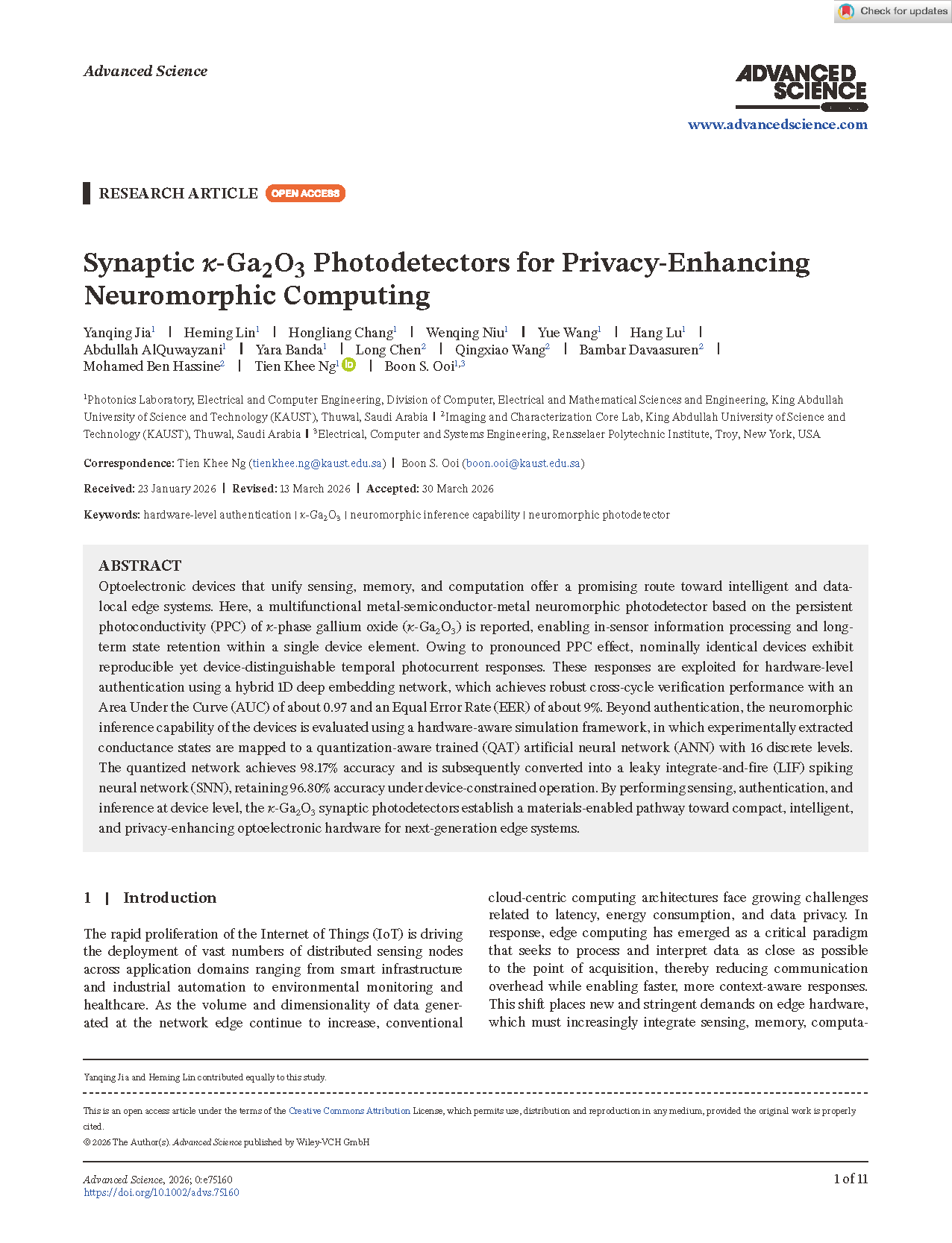
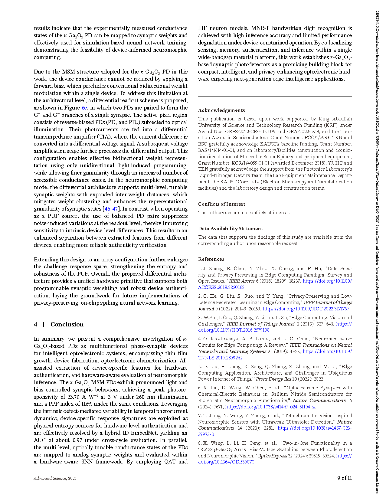
FIGURE 1. The device design concept, its structure, and PPC characterization. Schematic diagram of the functional classification of the device, including UV sensing, synaptic memory, device authentication and neuromorphic computing.
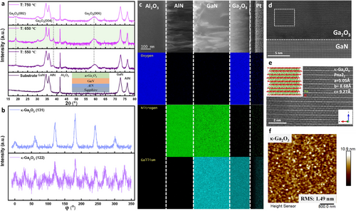
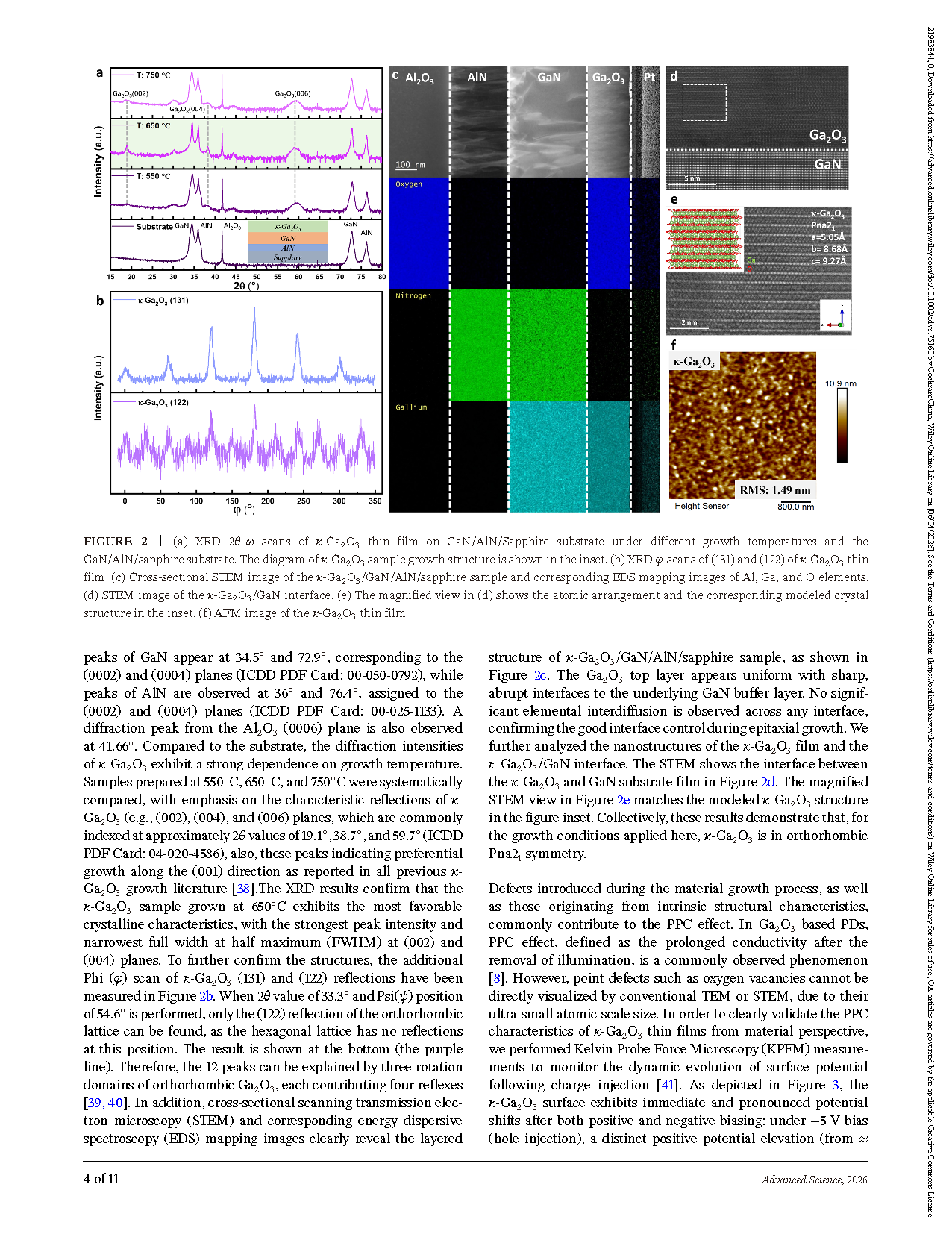
FIGURE 2. (a) XRD 2θ–ω scans of κ-Ga2O3 thin film on GaN/AlN/Sapphire substrate under different growth temperatures and the GaN/AlN/sapphire substrate. The diagram of κ-Ga2O3 sample growth structure is shown in the inset. (b) XRD φ-scans of (131) and (122) of κ-Ga2O3 thin film. (c) Cross-sectional STEM image of the κ-Ga2O3/GaN/AlN/sapphire sample and corresponding EDS mapping images of Al, Ga, and O elements. (d) STEM image of the κ-Ga2O3/GaN interface. (e) The magnified view in (d) shows the atomic arrangement and the corresponding modeled crystal structure in the inset. (f) AFM image of the κ-Ga2O3 thin film.
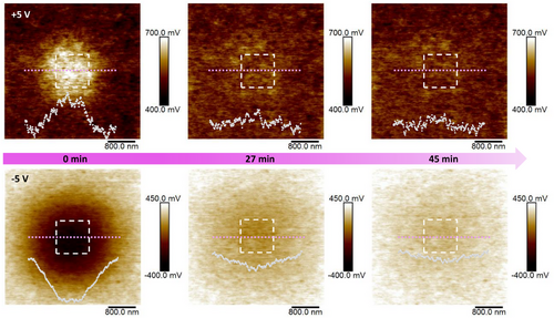
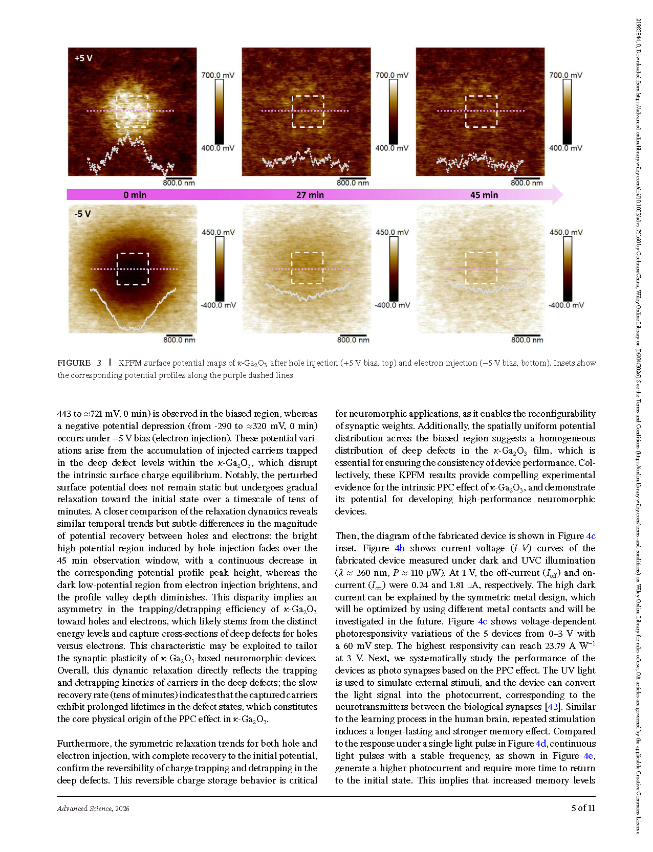
FIGURE 3. KPFM surface potential maps of κ-Ga2O3 after hole injection (+5 V bias, top) and electron injection (−5 V bias, bottom). Insets show the corresponding potential profiles along the purple dashed lines.
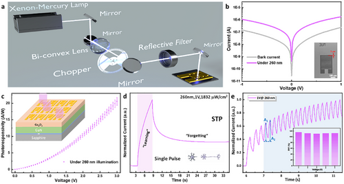
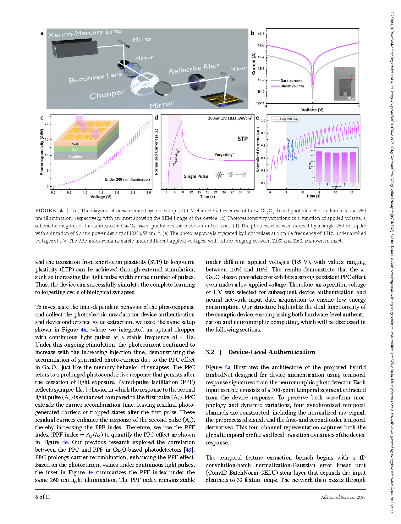
FIGURE 4. (a) The diagram of measurement system setup. (b) I–V characteristics curve of the κ-Ga2O3-based photodetector under dark and 260 nm illumination, respectively, with an inset showing the SEM image of the device. (c) Photoresponsivity variations as a function of applied voltage, a schematic diagram of the fabricated κ-Ga2O3-based photodetector is shown in the inset. (d) The photocurrent was induced by a single 260 nm spike with a duration of 5 s and power density of 1832 µW cm−2. (e) The photoresponse is triggered by light pulses at a stable frequency of 4 Hz, under applied voltages at 1 V. The PPF index remains stable under different applied voltages, with values ranging between 110% and 116% is shown in inset.
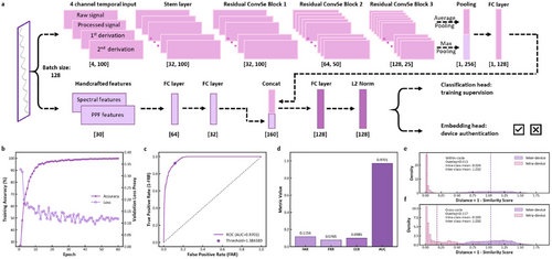
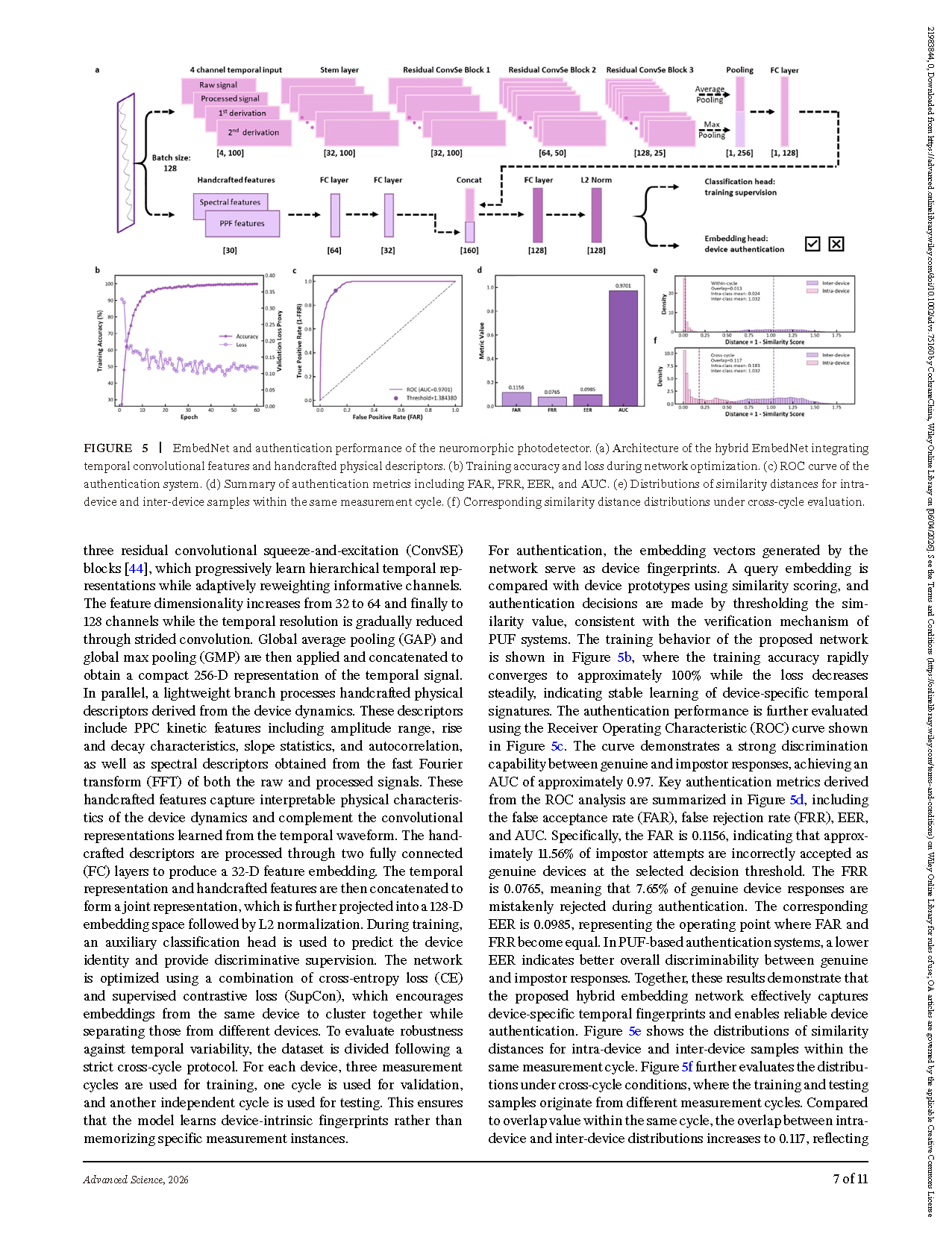
FIGURE 5. EmbedNet and authentication performance of the neuromorphic photodetector. (a) Architecture of the hybrid EmbedNet integrating temporal convolutional features and handcrafted physical descriptors. (b) Training accuracy and loss during network optimization. (c) ROC curve of the authentication system. (d) Summary of authentication metrics including FAR, FRR, EER, and AUC. (e) Distributions of similarity distances for intra-device and inter-device samples within the same measurement cycle. (f) Corresponding similarity distance distributions under cross-cycle evaluation.
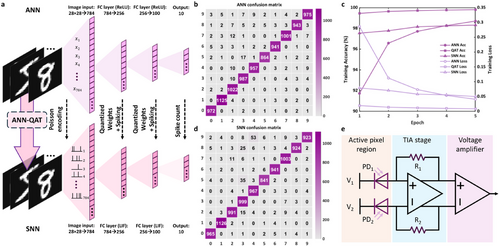
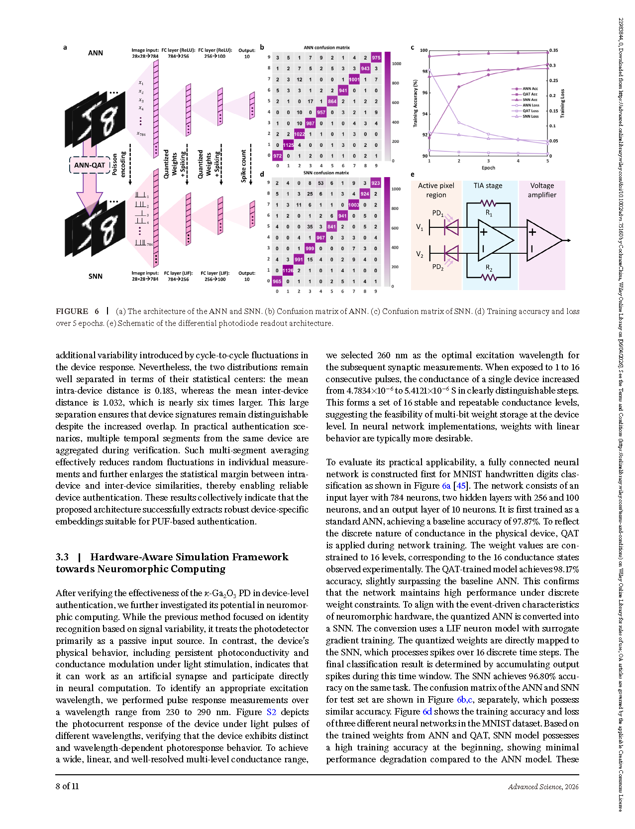
FIGURE 6. (a) The architecture of the ANN and SNN. (b) Confusion matrix of ANN. (c) Confusion matrix of SNN. (d) Training accuracy and loss over 5 epochs. (e) Schematic of the differential photodiode readout architecture.
DOI:
doi.org/10.1002/advs.75160