


News Trends
【Domestic News】Bring you close to Gallium Oxide —— Gallium Oxide Material Briefing
日期:2023-04-18阅读:1370
The Fourth Generation Wide Band Gap Semiconductor Materials
Currently, gallium oxide (Ga2O3), as a "ultra wide band gap semiconductor" material, has received continuous attention. Ultra-wide band gap semiconductors also belong to the "fourth generation semiconductors". Compared with the third generation semiconductors silicon carbide (SiC) and gallium nitride (GaN), the band gap width of gallium oxide is up to 4.9 eV, which is higher than 3.2 eV of silicon carbide and 3.39 eV of gallium nitride. The wider band gap width means that electrons need more energy to transition from the valence band to the conduction band, so gallium oxide has the characteristics of high breakdown voltage, high temperature resistance, high power, and radiation resistance. In addition, under the same specification, the wide band gap material can manufacture devices with smaller die size and higher power density, and save the supporting heat dissipation and wafer area, and further reduce the cost. In August 2022, the Bureau of Industry Security (BIS) of the United States Department of Commerce implemented export control on the fourth generation semiconductor materials--gallium oxide and diamond, and believed that the application of gallium oxide's high pressure resistance in the military field was crucial to the national security of the United States. Since then, gallium oxide has attracted more attention in global scientific research and industry.
01 Performance, Application, and Cost of Gallium Oxide
1.1 the Fourth Generation of Semiconductor Materials
The first generation of semiconductors refer to elemental semiconductor materials such as silicon (Si) and germanium (Ge); The second generation semiconductors refer to semiconductor materials such as gallium arsenide (GaAs) and indium phosphide (InP) that have high mobility; The third generation of semiconductors refer to wide band gap semiconductor materials such as silicon carbide (SiC) and gallium nitride (GaN); The fourth generation of semiconductors refer to ultra wide band gap semiconductor materials such as gallium oxide (Ga2O3), diamond (C), aluminum nitride (AlN), and ultra narrow band gap semiconductor materials such as gallium antimonide (GaSb) and indium antimonide (InSb). The fourth generation ultra wide band gap materials overlap with the third generation semiconductor materials in application, and have more prominent application advantages mainly in the field of power devices. The fourth generation of ultra narrow band gap materials are mainly used in infrared detection, lasers, and other fields due to their high electron mobility and easy excitation transitions. The fourth generation of semiconductors are all on the "strategic electronic materials" list of the Ministry of Science and Technology of China. Many specifications are subject to foreign embargo and domestic export ban, making them a highland for global semiconductor technology competition. The core difficulty of the fourth generation semiconductor lies in material preparation, and breakthroughs in the material end will gain great market value.
1.2 Crystal Structure and Properties of Gallium Oxide
There has five allotropes of gallium oxide---α, β, γ, ε and δ, among which, β-Ga2O3 (β phase gallium oxide) is the most stable. When heated to a certain high temperature, all other metastable states are converted to β phase, and it is for sure to be β phase at the melting point of 1800℃. At present, the industrialization is mainly β phase gallium oxide.
Material Properties of Gallium Oxide
- Ultra-wide band gap. Gallium oxide is stable in extreme environments such as ultra-low temperature and strong radiation. Matching deep ultraviolet absorption spectrum, it is used in solar-blind ultraviolet detector.
-
High breakdown field strength, high Baliga value. Matching high breakdown voltage and low loss, it is an irreplaceable star material for high voltage and high power devices.
Note: Since solar-blind ultraviolet devices mainly use gallium oxide thin film, gallium oxide in this report in particular refers to the single crystal substrate, so the application of gallium oxide in power devices, RF devices and other fields is mainly discussed.

1.3 Gallium Oxide: a Challenge to Silicon Carbide
Gallium oxide is the only material in wide band semiconductor that can be grown by liquid melt, with its advantages over silicon carbide, such as low hardness,and low cost of material growth and processing. Gallium oxide will comprehensively challenge silicon carbide.
1、Gallium oxide has good power performance and low loss
The Baliga value of gallium oxide is four and ten times that of GaN and SiC, respectively, with good conduction characteristics. The power loss of gallium oxide devices is 1 / 7 of that of SiC, or 1 / 49 of that of silicon-based devices.
2、The cost of processing gallium oxide is low
Gallium oxide is softer than silicon, so it is less difficult to process, while SiC has high hardness and high processing cost.
3、Gallium oxide is of good crystal quality
Gallium oxide is grown by liquid melt, with dislocations (number of defects per square centimeter) <102cm-2, while SiC is grown by vapor phase, with dislocations about 105cm-2.
4、Gallium oxide grows 100 times faster than SiC
Gallium oxide is grown by liquid melt, 10~30mm per hour, 2 days per furnace, while SiC is grown by vapor phase, 0.1~0.3mm per hour, 7 days per furnace.
5、The cost of production line of gallium oxide wafer is low, the production is fast
The wafer production line of gallium oxide is very similar to that of Si, GaN and SiC, and the conversion cost is low, which is conducive to accelerating the industrialization progress of gallium oxide. "For the first time in the world, Novel Crystal Technology has successfully produced 100 mm wafers made of gallium oxide, a new generation of power semiconductor material. And customers can manufacture a new generation of products with existing equipment that supports 100 mm wafers, effectively using the old equipment invested in the past." from the original report by Nihon Keizai Shimbun, unlike SiC, which requires special equipment and has to build new production lines, the potential convertible capacity of gallium oxide is huge.
1.4 Application of Gallium Oxide: Power Devices
Four major opportunities for gallium oxide:
- Unipolar replacement bipolar: MOSFET replaces IGBT. In the power markets such as new energy vehicles and charging piles, UHV, fast charging, industrial power supply, motor control, the elimination of silicon-based IGBT is inevitable, while silicon-based GaN, SiC, Ga2O3 are competitive materials.
-
More energy saving and more efficient: gallium oxide power devices have low energy consumption, in line with the strategy of carbon neutrality and carbon peak.
-
Easy to achieve mass production of large size: diameter expansion, simple production, chip process are easy to achieve, with low cost.
-
High reliability requirements: the material properties are stable, with reliable structure, high quality substrate / epitaxy.
Target market for gallium oxide:
-
In the long term, gallium oxide power devices cover 650V / 1200V / 1700V / 3300V, which is expected to fully penetrate the field of on-board and electrical equipment from 2025-2030. In the future, it will also play advantages in the exclusive market of ultra-high voltage gallium oxide, such as high voltage power vacuum tube and other application fields.
-
In the short term, gallium oxide power devices are expected to take the lead in medium and high voltage markets which is low-threshold and cost-sensitive, such as consumer electronics, home appliances and industrial power supplies that can use high reliability and high performance of materials.
the market that gallium oxide is easy to win:
-
New energy vehicle OBC / inverter / charging pile
-
DC / DC: 12V / 5V 48V conversion
-
Storage market for IGBT

Figure: Market forecast of gallium oxide in power devices
1.5 Application of Gallium Oxide: RF Devices
The market of GaN needs substrates of large size and low cost, to really play the advantages of GaN materials.
The quality of epitaxial layer grown on homogeneous substrate is the best. Yet, due to the high price of the GaN substrate, relatively cheap substrate are often used in the LED, consumer electronics, radio frequency, such as Si, sapphire, SiC substrate. But the structure differences between substrate and GaN crystal will cause lattice mismatch, which is equivalent to sacrificing epitaxial quality with maintenance cost. When GaN is homogeneous and epitaxial GaN, it can be used in the more demanding application scenarios such as laser.
The lattice mismatch of GaN with gallium oxide is only 2.6%. With gallium oxide substrate, GaN from heteroepitaxial growth is of high quality, and the cost of 6 inch gallium oxide grown without iridium is close to silicon, which is expected to be significantly applied in the GaN RF device market.

Figure: A 2-inch Synoptics gallium oxide transistor with a GaN epitaxial layer

Table: substrate material comparison of GaN epitaxy
1.6 Industry-related Policies on Gallium Oxide
The American embargoes, localization is called for: On August 12,2022, the US Bureau of Industrial Security (BIS) of Commerce imposed export controls on the fourth-generation semiconductor materials gallium oxide (Ga2O3) and diamond, believing that the application of its high breakdown voltage in the military field is crucial to the national security of the United States.
02 Crystal Growth and Epitaxial Process of Gallium Oxide Substrate
2.1 Crystal Growth Process of Semiconductor Materials
Melt growth method is the most ideal way to grow semiconductor materials, which has the following advantages.
-
Large size: small seed crystals can grow into large crystals
-
High yield: each furnace crystal ingot can be cut out to get thousands of pieces of substrate
- Good quality: dislocation can tend to 0, with great crystal quality
- Grow fast: it can grow several centimeters per hour, much faster than the vapor phase method
Gallium oxide is the only material in wide band gap semiconductor with atmospheric pressure liquid, which can be grown by melt growth method. The Czochralski growth commonly used for gallium oxide growth is a melt growth method, which relies on iridium crucible (precious metal Ir). The reason is that gallium oxide growth requires high temperature oxygen-rich environment, otherwise the raw materials are easy to decompose into Ga and O2, affecting the quality of products, while only the precious metal iridium crucible can remain stable in this extreme environment.

Figure: Diagram of growing gallium oxide by Czochralski growth
2.2 Crystal Growth Process of Gallium Oxide
Due to the high volatilization of raw materials, the crystal growth process of gallium oxide has gradually evolved from the Czochralski growth method to the edge-defined film-fed growth method with iridium cover and mold. Both methods need to use iridium crucible. At present, the edge-defined film-fed growth method has become the mainstream method for gallium oxide crystal growth. However, due to the high cost and high loss of iridium crucible, it will be subject to corrosion loss after growing dozens of furnaces, which needs to be melted and processed again. In the process of crystal growth, iridium will form impurities into the crystal, and the industry has a strong demand for the development without iridium. In April 2022, Nippon Keizai Shimbun released a message that Japan C & A company uses a copper crucible when applying the edge-defined film-fed growth method to grow 2 inches of gallium oxide single crystal, which can reduce the cost to 1 / 100 of the guide method.

Figure: Two diagrams of gallium oxide growth with iridium method and its gallium oxide single crystal product: (left) the Czochralski growth method; (right) the edge-defined film-fed growth method

Figure: gallium oxide single crystal prepared without iridium
The process of gallium oxide growth starts from the melting and pulling of the raw material in the crucible, and then goes through the process of cutting, grinding and polishing, forming the gallium oxide single crystal substrate. After the epitaxial process, the homogeneous epitaxial or heteroepitaxial structure is obtained, and finally is processed into gallium oxide wafer.

Figure: Process of gallium oxide without iridium method and EFG
2.3 Costs Comparison---Iridium Involved, and Iridium Uninvolved
-
Method involved Iridium: The National Renewable Energy Laboratory (NREL) predicts that the cost of gallium oxide is $283 (2,000 yuan) without additional wafer manufacturing process optimization, which will be reduced to $195 with various cost-saving measures. Iridium crucible and its loss occupy more than half.
-
Method free from Iridium: Japan's C & A company reported the achievements of the 2-inch iridium uninvolved, claiming that the cost could drop significantly to 1 / 100 of EFG method.

Figure: Cost analysis of growing gallium oxide substrate with iridium involved
2.4 Gallium Oxide Homoepitaxy
The rate of gallium oxide epitaxy is related to the crystal orientation of the substrate. (100) surface homogeneous epitaxy is the most difficult, while (001) and (010) surfaces are easier, so in the epitaxy and device process, the gallium oxide substrate of (001) or (010) surface is basically selected. The dominant surface obtained from Melt Growth Method is (010) radial surface, but the current mainstream EFG method can only obtain narrow rectangular wafer, the side (100) surface is the most easy to obtain large size. In order to get valuable (001) and (010) surface, large thickness crystal must be prepared for cutting from a bevel angle, but large thickness crystal process is difficult to achieve. It is only Japan that reported the achievement of more than 10mm thickness crystal. So currently it is only Japan that can supply (001) and (010) surface substrate. In 2014, Tokyo A & M University obtained large size epitaxial film for the first time in (001) surface. At the same time, from 2012 to 2015, the size of β-Ga2O3 large wafer was increased to 4 inches. The epitaxial process of gallium oxide promoted the development of devices and really opened the application of gallium oxide power devices. This requires gallium oxide substrate manufacturers to be able to provide multi-specification crystal surface products. At present, gallium oxide epitaxial process has 2 methods--- HVPE (halide vapour phase epitaxy) and MOCVD (metal organic chemical vapor deposition). HVPE equipment can deposit thick film, with fast film growth speed and low equipment cost, but relevant equipment has been prohibited from being imported from abroad. China's industry is calling for the ability of localization. NCT of Japan has achieved a 6-inch gallium oxide epitaxy process by HVPE.
2.5 Doping and Device Applications of Gallium Oxide
Similar to SiC, gallium oxide also has conductive and semi-insulating substrates, obtained by doping different elements, and have different applications in power devices.

Figure: Gallium oxide single crystal (left) doped Si, N-type conduction; (middle) unintentional doping, N-type high resistance; (right) doped Mg, insulation

Figure: (left) A typical gallium oxide SBD vertical structure with a Si-doped conductive substrate; (right) a typical gallium oxide MOSFET planar structure with a Fe-doped insulating substrate
03 Academic Research and Application Development of Gallium Oxide
3.1 Competition of Gallium Oxide Substrate
It took 20 years to develop SiC from 2 inches to 6 inches (1992-2012), while gallium oxide, from 2 inches to 6 inches, was just 4 years (2014-2018).
-
Home: CLP 46 set a domestic record of 4-inch gallium oxide in 2018, and Shandong University also reported an achievement of 4-inch in 2022. At present, there is no company or university with mass production capacity in China, which limits the cost of iridium crucible to some extent.

Figure: progress of gallium oxide substrate on size at home and abroad
3.2 Competition on Gallium Oxide Device
- USA: The device research results in the United States are the most outstanding, and various innovative structures and processes have greatly promoted the progress of gallium oxide devices.
- Japan: Thanks to the domestic supply of substrate and epitaxial tablets, the domestic gallium oxide industry chain was first formed in Japan.
- China: With the progress of substrate and epitaxial development in China, the device-related results have also reached the international level.

Figure: Progress of gallium oxide MOSFET devices at home and abroad
3.3 Research on the Disadvantages of Gallium Oxide Materials
1、To Solve the Problem of Low Thermal Conductivity
Though the heat dissipation challenges the R&D of gallium oxide, it is a problem that can be solved by engineering and does not constitute an obstacle to industrialization. As shown in the figure below, Virginia Tech solves the heat dissipation problem through the packaging method of double-sided silver sintering, and can conduct the heat generated at the Schottky junction---the thermal resistance at the junction is 0.5K / W, at the bottom 1.43, and the transient surge current is up to 70A.

Figure: The device structure of Virginia Tech University adopts the package method of double-sided silver sintering to solve the heat dissipation problem
2、To Solve Type-P Doping
The valence band of gallium oxide band structure cannot effectively conduct hole conduction, making it difficult to manufacture P-type semiconductors. Recently, teams such as Stanford and Fudan have implemented gallium oxide P-type devices in the laboratory and are expected to gradually introduce them into industrial applications. As shown in the figure below, In August 2022, Stanford University published the results of achieving a P-type vertical structure of gallium oxide in the laboratory. The PN junction was formed through Mg SOG magnesium diffusion, with a switching voltage of 7V and a switching speed of 109.

Figure: Device structure of Stanford University, forming a suspected p-n junction in the laboratory
04 Industrial Chain and Market Space of Gallium Oxide
4.1 Industry Chain of Gallium Oxide
Gallium oxide substrate and epitaxial link are located upstream of the power device industry chain. Analogous to the silicon carbide industry chain, the value is concentrated in the upstream substrate and epitaxial links: of the cost of one silicon carbide device, 47% comes from the substrate, 23% comes from the epitaxial, and the substrate + epitaxial accounts for 70% together. As the cost of gallium oxide decreases further, the substrate proportion will be much smaller than the SiC.

Figure: Industrial chain of gallium oxide
4.2 Gallium Oxide in the Power Device Market
FLOSFIA, a well-known enterprise in the field of gallium oxide in Japan, expects that the market size of gallium oxide power devices will begin to exceed GaN in 2025 and reach $1.542 billion US dollars (about 10 billion yuan) in 2030, reaching 40% of SiC and 1.56 times of GaN. (Note: FLOSFIA's forecast is more conservative than Yole's. Yole forecasts the silicon carbide power device market capacity of $6.297 billion in 2027 and FLOSFIA forecasts $3.845 billion in 2030.)
Only in terms of new energy vehicle market, in 2021, 6.5 million new energy vehicles were sold worldwide, whose permeability is 14.8%, while the permeability of silicon carbide is 9%. With the increase of the permeability rate of new energy vehicles, the market size will gradually expand. At present, SiC and GaN are far from being able to sway the market. By contrast, the access of the development of gallium oxide is very abundant.

Figure: Global power device market and Gallium oxide power device market size ($1 million)
4.3 Gallium Oxide in the Market for RF Devices
The market capacity of gallium oxide in RF devices can refer to the market of silicon carbide epitaxial gallium nitride devices. SiC Semi-insulating substrates are mainly used in 5G base stations, satellite communications, radar and other directions. In 2020, the market size of SiC epitaxial GaN RF devices is about $891 million, and will grow to $2.222 billion (about 15 billion yuan) in 2026.
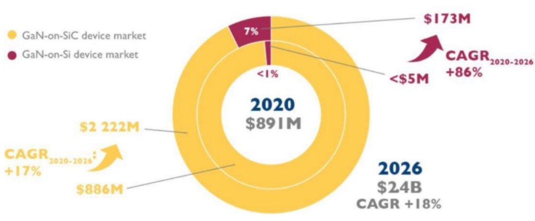
Figure: Market size of silicon carbide epitaxial gallium nitride devices ($1 million)
05 Competition Pattern and Industrialization Progress of Gallium Oxide
Japan: The Whole IDM Industry Chain Leads the World
Internationally, only Japan has developed mass production and started industrialized applications, and the main application fields are industrial power supply, industrial motor control, etc., And the industrial side takes Yaskawa and Satori as the main representatives. Japan is expected to mass-produce gallium oxide power devices in 2023:
- Japan’s NCT has made device samples on the Ga2O3 experimental line and is building a mass production line, which is scheduled to start mass production in 2023.
- Japan's FLOSFIA will, before the second quarter of 2023, produce hundreds of thousands of gallium oxide devices per month to auto parts manufacturers and other sales.
- Tamura, a Japanese electronics parts manufacturer, will also start production at tens of thousands of units a month in 2024 and increase production capacity to about 60 million units a month by 2027.

Figure: Market Strategy of FLOSFIA's Gallium Oxide Power Device
USA: the Research on Gallium Oxide Devices are the most Advanced
Only Kyma currently has a 1-inch substrate in the United States, whose single crystal size lags behind China, and the industrial chain is relatively blank. However, the achievements on device are very outstanding, with strong innovation ability. Various innovative structures and processes have greatly promoted the progress of gallium oxide devices.
China: The Substrate Link Closely Follows Japan
China's gallium oxide substrate can be supplied in small batches, and the industrialization process of extension and devices are almost blank. The main force and outstanding achievements of research and development are all in universities and research institutes. However, China's gallium oxide research and development of gallium oxide devices is in the world Top 3. In terms of IP, China reversed the passive situation in the SiC field. The current industrial stage of gallium oxide is similar to the state of SiC before the launch of the Tesla Model 3, and the technology reserve has been completed, waiting for a landmark event to ignite the market.
In general, in the next 10 years, gallium oxide devices are likely to become power electronics devices that compete directly with silicon carbide, but as a new semiconductor material, the breakthrough of the gallium oxide market size depends on the rapid cost reduction. The next few years will be a key stage for Japan to introduce gallium oxide on a large scale. Whether China can follow up with the footsteps of the industry requires the domestic gallium oxide industry to work together.
