Paper Sharing
【Member Papers】Vertical β-Ga₂O₃ Schottky barrier diodes with low surface roughness
日期:2026-04-09阅读:252
Researchers from Shenzhen Pinghu Laboratory and Southern University of Science and Technology have published a dissertation titled " Vertical β-Ga2O3 Schottky barrier diodes with low surface roughness " in Journal Of Vacuum Science & Technology A.
Background
β-Ga2O3 has gained significant recognition as an ultra-wide bandgap (4.9eV) semiconductor material for developing next generation power electronics owing to its large breakdown electric field of 8 MV/cm and high-temperature stability. Furthermore, β-Ga2O3 has been demonstrated to facilitate available melt-grown substrates, which enables high-quality homoepitaxy as well as potentially a low-cost device platform. For homoepitaxial thin-film growth of β-Ga2O3, the principal (100), (010), and (001) planes are commonly employed. The (001) plane serves as a cleavage plane, enabling the production of large-diameter (>6in.) commercial wafers. This significantly reduces wafer processing difficulty and cost and provides a critical material foundation for the mass pro duction of high-performance power electronic devices. Therefore, Ga2O3-based power rectifiers, such as Schottky barrier diodes (SBDs), combine high breakdown strength with low conduction loss and competitive manufacturing costs, enabling outstanding performance in high-power-density applications.
Abstract
We investigate the properties of the β-Ga2O3 Schottky barrier diodes (SBDs) fabricated on halide vapor phase epitaxy-grown (001)-oriented β-Ga2O3 epilayers with various surface treatment techniques. The surface etching methods employed include two-step inductively coupled plasma (ICP) etching, wet etching, and two-step dry etching followed by wet etching. Combining atomic force microscopy and x-ray photo electron spectroscopy, we found that the surface roughness and oxygen vacancies (VO) in the epilayers were significantly reduced by employing a two-step ICP etching followed by wet etching. The optimized surface exhibits a root-mean-square roughness of 0.12 nm and a step-flow morphology. The SBDs fabricated on the optimized epilayers achieve a comprehensively enhanced performance, with a breakdown voltage of 1675 V, a near-ideal ideality factor of 1.05, and a power figure of merit of 467 MW/cm2.
Conclusion
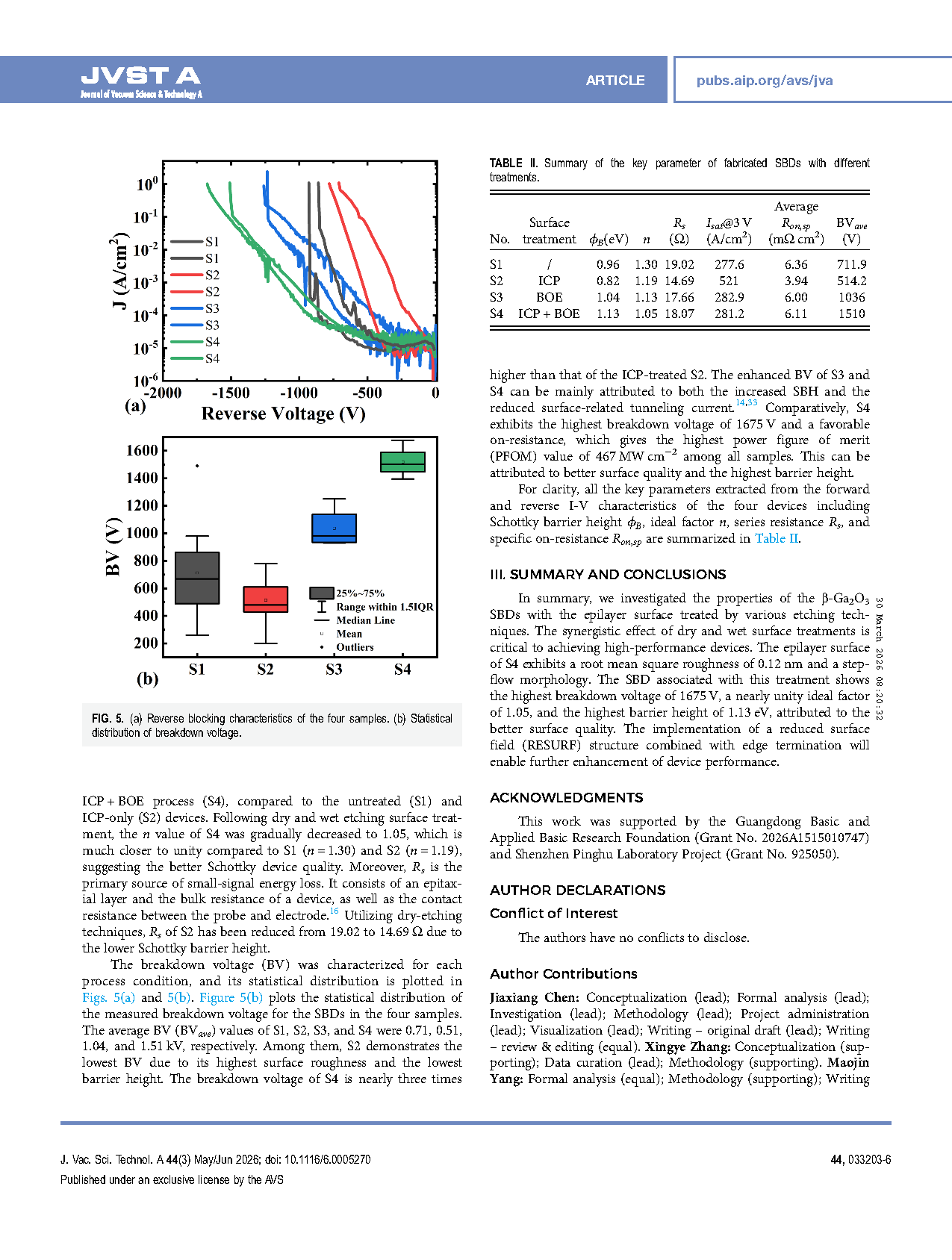
In summary, we investigated the properties of the β-Ga2O3 SBDs with the epilayer surface treated by various etching tech niques. The synergistic effect of dry and wet surface treatments is critical to achieving high-performance devices. The epilayer surface of S4 exhibits a root mean square roughness of 0.12nm and a step flow morphology. The SBD associated with this treatment shows the highest breakdown voltage of 1675 V, a nearly unity ideal factor of 1.05, and the highest barrier height of 1.13 eV, attributed to the better surface quality. The implementation of a reduced surface field (RESURF) structure combined with edge termination will enable further enhancement of device performance.
Project Support
This work was supported by the Guangdong Basic and Applied Basic Research Foundation (Grant No. 2026A1515010747) and Shenzhen Pinghu Laboratory Project (Grant No. 925050).
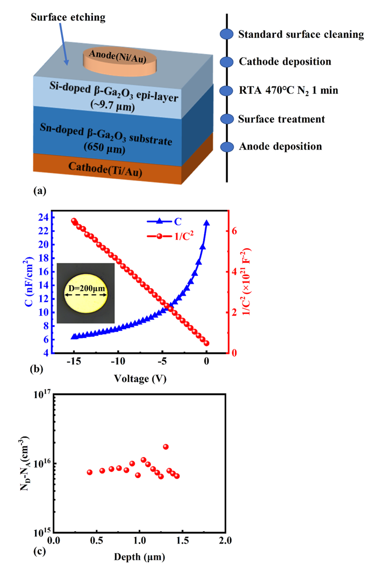
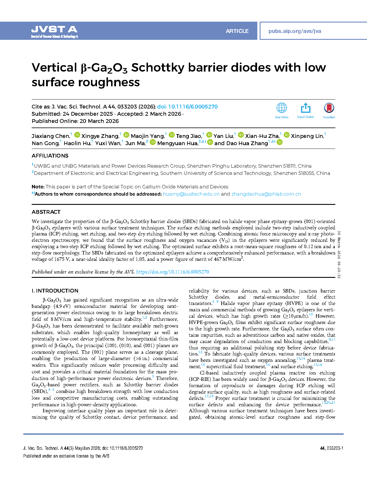
FIG. 1. (a)Process flow of the β-Ga2O3 SBD fabrication of sample 4 (S4). (b)C-V characteristic. (c)Carrier concentration depth profile extracted from 1/C2-V characteristics.
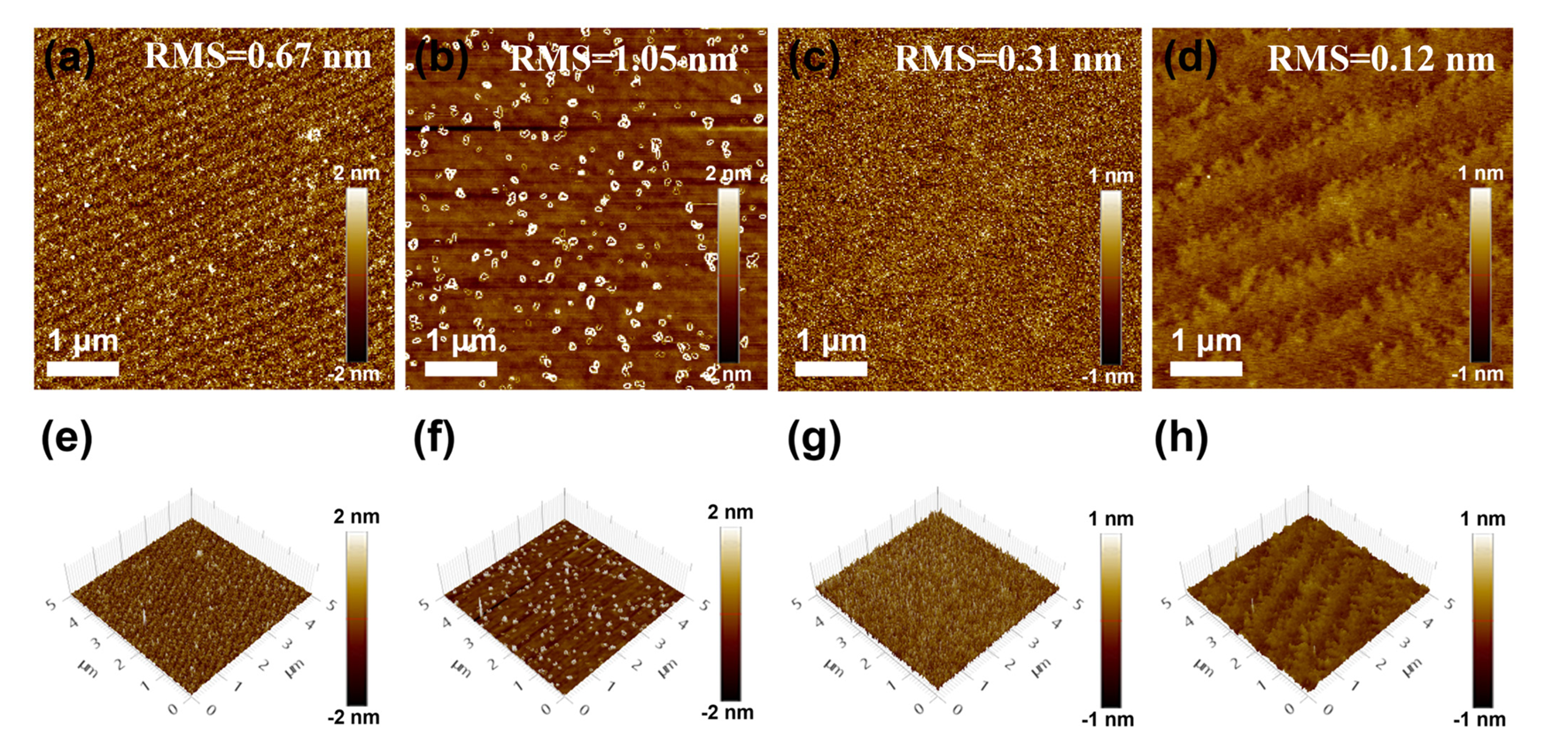
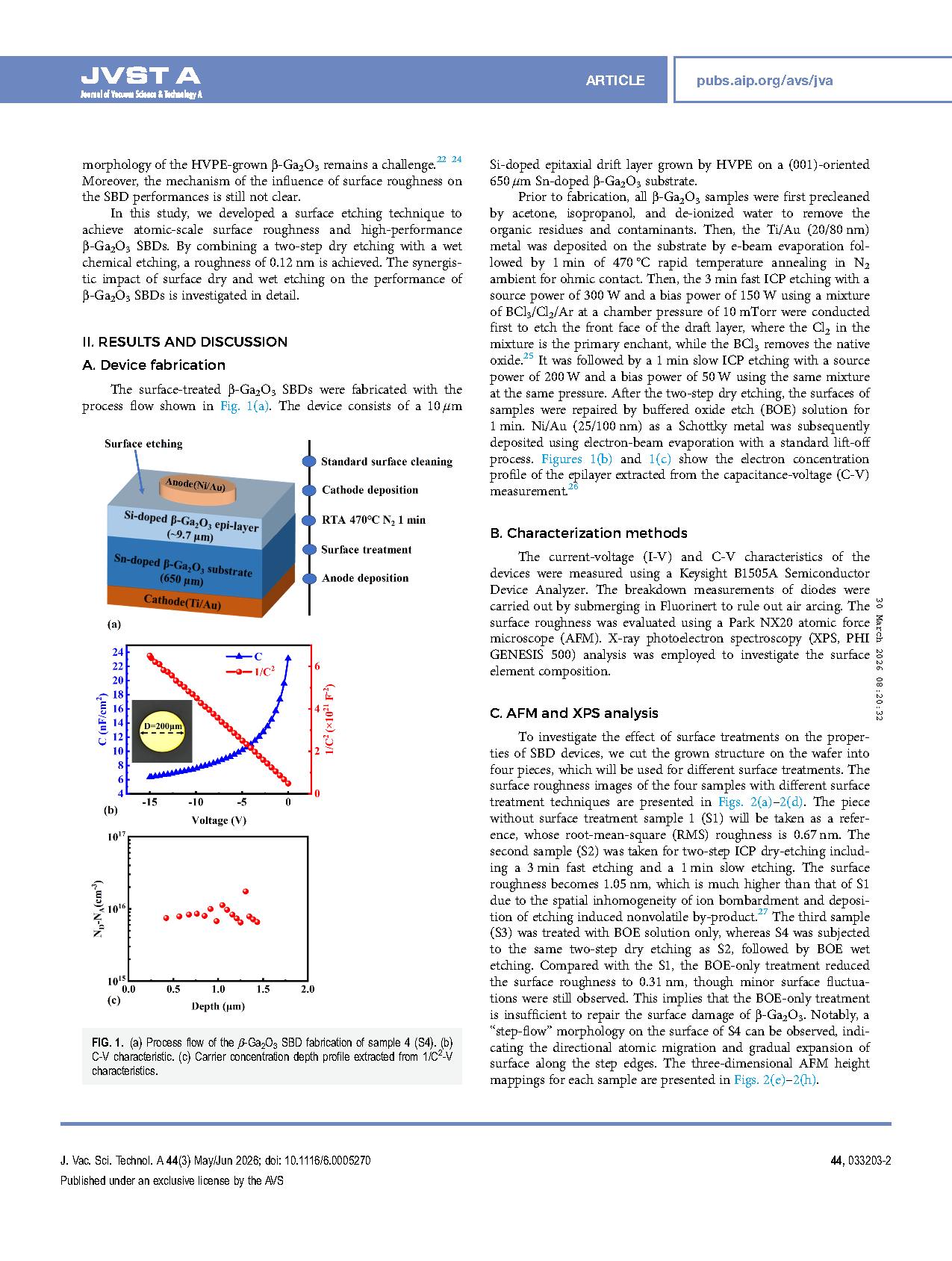
FIG. 2. AFM images in 5×5 μm2 area showing surface rough ness and morphologies of β-Ga2O3 samples (a) S1 without treatment, (b) S2 with only two-step ICP dry etching,(c) S3 with only BOE treatment, and (d) S4 with two-step dry etching plus wet treatment. (e)–(h) Three-dimensional AFM mapping of S1-S4.
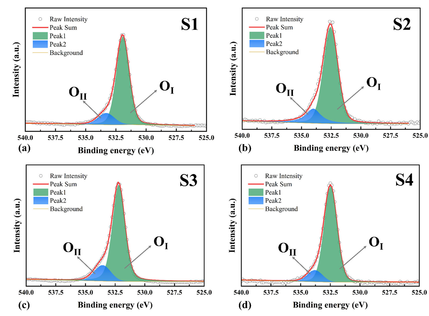
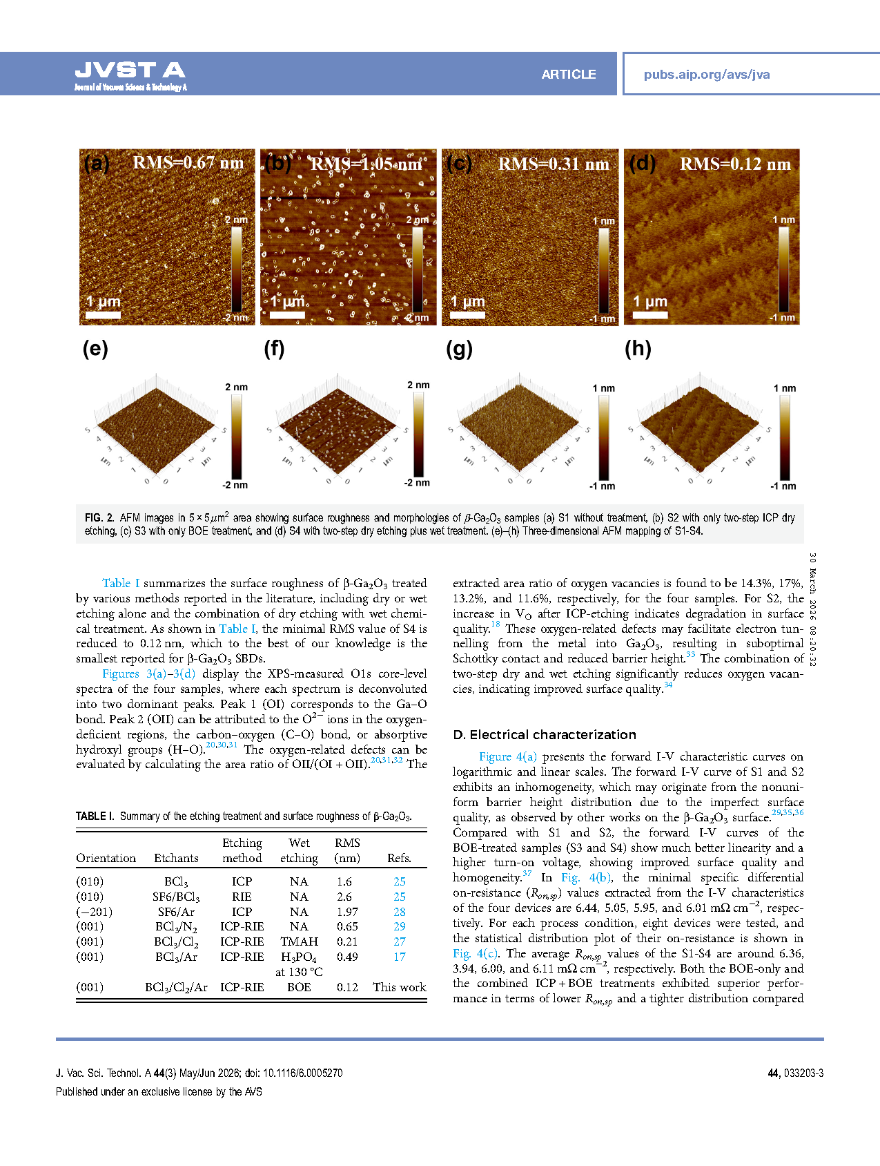
FIG. 3. Area ratio variations of OII/(OI + OII) for samples (a) S1 (14.3%), (b) S2 (17%), (c) S3 (13.2%), and (d) S4 (11.6%) in XPS spectra.
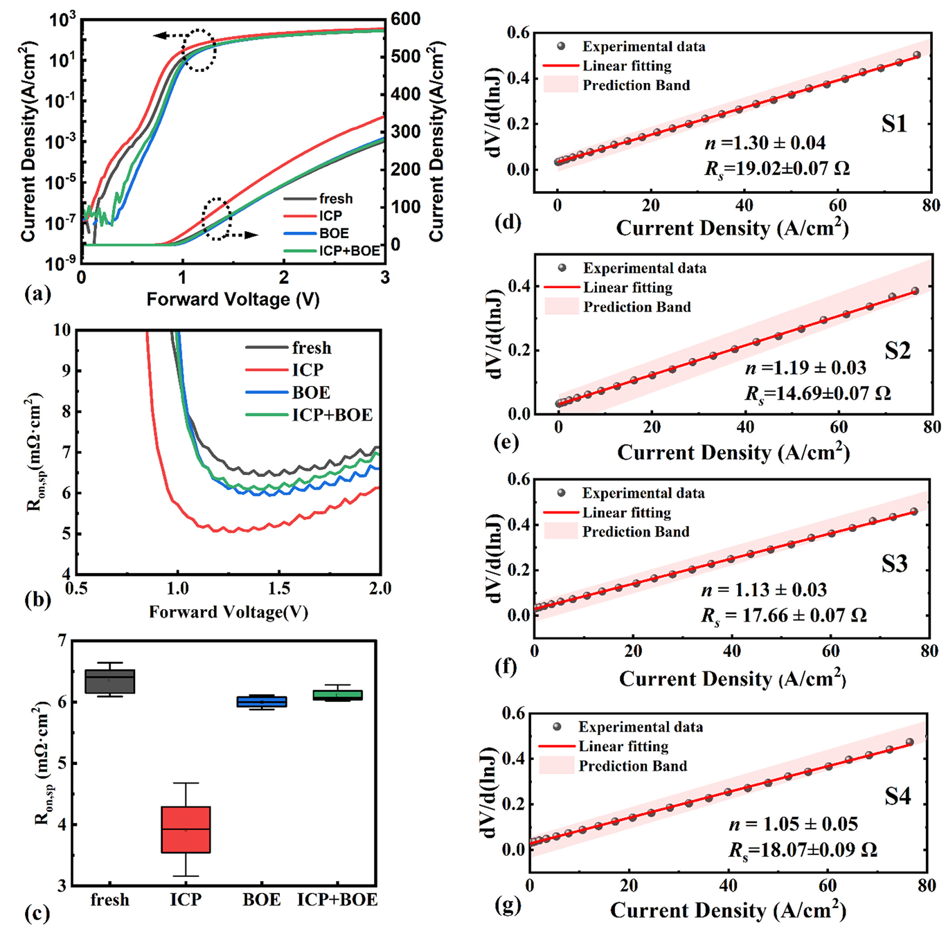
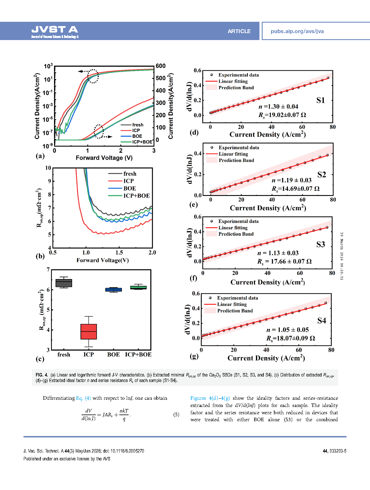
FIG. 4. (a)Linear and logarithmic forward J-V characteristics. (b)Extracted minimal Ron,sp of the Ga2O3 SBDs (S1, S2, S3, and S4). (c)Distribution of extracted Ron,sp. (d)–(g)Extracted ideal factor n and series resistance Rs of each sample (S1-S4).
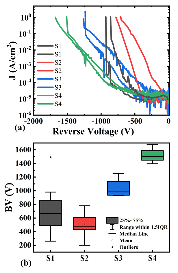
FIG. 5. (a)Reverse blocking characteristics of the four samples. (b)Statistical distribution of breakdown voltage.
DOI:
doi.org/10.1116/6.0005270