Paper Sharing
【Domestic Papers】Performance study of ultraviolet photodetector based on gallium oxide thin film
日期:2026-04-10阅读:290
Researchers from the Xi’an University of Posts & Telecommunications have published a dissertation titled "Performance study of ultraviolet photodetector based on gallium oxide thin film" in Transducer and Microsystem Technologies.
Background
Gallium oxide (Ga₂O₃) possesses a wide bandgap and a high breakdown electric field, and exhibits strong sensitivity to O₂ and solar-blind ultraviolet (UV) radiation. In addition, it offers several advantages, including high electron mobility, low dielectric constant, excellent chemical and physical stability, and high mechanical strength. Owing to these properties, Ga₂O₃ has attracted considerable interest for applications in power semiconductor devices, gas sensors, and solar-blind UV photodetectors, making it a promising multifunctional wide-bandgap semiconductor material. Among its polymorphs, β-Ga₂O₃ has a bandgap of approximately 4.8 eV, corresponding to an absorption wavelength around 254 nm, which matches well with the photon energy in the solar-blind UV region, thus making it an ideal material for solar-blind UV detection.
In recent years, Ga₂O₃ thin films have become an international research hotspot due to their relatively simple fabrication processes, low cost, and excellent material properties. Various techniques have been employed to prepare Ga₂O₃ thin films, including molecular beam epitaxy (MBE), chemical vapor deposition (CVD), physical vapor deposition (PVD), and atomic layer deposition (ALD). Among these methods, ALD offers several advantages such as precise step coverage, excellent uniformity over large areas, and atomic-scale thickness control. Previous studies have shown that 250 °C is the optimal growth temperature for Ga₂O₃ thin films deposited by ALD, and photodetectors fabricated from such films exhibit fast response characteristics, with rise and decay times of 539 ns and 89 ms, respectively. In addition, β-Ga₂O₃ thin films prepared by pulsed laser deposition (PLD) or PVD have also been used to fabricate metal–semiconductor–metal (MSM) structured solar-blind UV photodetectors. Although some devices demonstrate extremely low dark currents or high responsivity, relatively slow response times remain a challenge.
Based on these considerations, in this work Ga₂O₃ thin films were grown on Al₂O₃ substrates using the ALD technique, and the film quality was evaluated using X-ray diffraction (XRD). MSM photodetectors with interdigital electrode structures were subsequently fabricated. Rapid thermal annealing at 550 °C for 90 s was performed, and the effects of interdigital spacing, light intensity, and annealing treatment on the device performance were systematically investigated.
Abstract
A 130 nm thin film of β-Ga₂O₃ is grown on a sapphire (Al₂O₃) substrate by atomic layer deposition (ALD), and X-ray diffraction (XRD) test is conducted on the thin film to verify its quality. Metal–semiconductor–metal (MSM) photoconductive photodetectors with an interdigital structure are prepared on the grown film. The device has an ultra-low dark current of 100 fA and an ultra-high photo-to-dark current ratio (PDCR) of 1 × 10⁶. After rapid annealing of the device, it has an ultra-high photocurrent of 58 μA and better device ohmic contacts, but both the light and dark currents increase, the PDCR decreases an order-of-magnitude, the thin film resistance increases, the electron scattering ability is enhanced, and the device performance becomes weaker compared to that before annealing. Finally, the effect of interdigital spacing and light intensity on device performance after annealing is studied.
Conclusion
In this work, a 50 nm β-Ga₂O₃ thin film was grown on an Al₂O₃ substrate by atomic layer deposition (ALD), and MSM photodetectors with interdigital electrodes were fabricated on the grown film. The effects of different light intensities and interdigital spacings before annealing on the device characteristics were investigated. Rapid thermal annealing was carried out at 550 °C for 90 s, and the performance differences before and after annealing were compared. The influence of interdigital spacing and light intensity on the PDCR, responsivity, EQE, and D* of the devices was also analyzed.
The results show that the devices exhibit low dark current and photocurrent before annealing. After annealing, the photoresponse of the MSM device deteriorates, accompanied by recrystallization of the thin film, degradation of the crystal structure, enhanced electron scattering, and reduced carrier mobility, which leads to a decrease in PDCR. Meanwhile, the I–V curves after annealing show higher linearity, indicating improved ohmic contacts. However, the PDCR decreases by one order of magnitude.
Overall, the device exhibits an ultra-high PDCR of 1 × 10⁷ before annealing. After annealing, the device shows an ultra-high responsivity of 1.2 × 10³ A/W and a PDCR of 6 × 10⁴. In addition, the interdigital spacing affects device performance: as the spacing increases, both the photocurrent and dark current decrease, and the responsivity and EQE decrease with increasing spacing. For the same interdigital spacing, higher light intensity leads to larger photocurrent and dark current, as well as increased PDCR, EQE, responsivity, and D*.
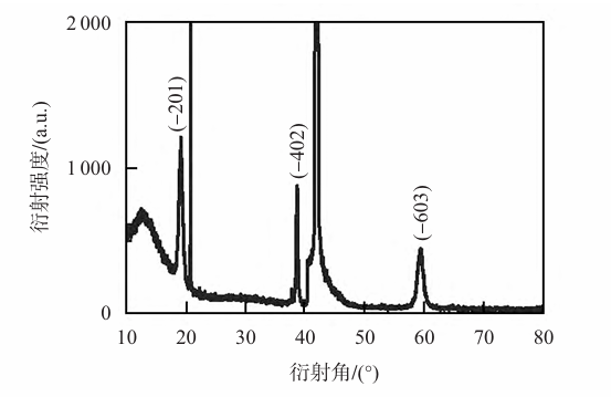
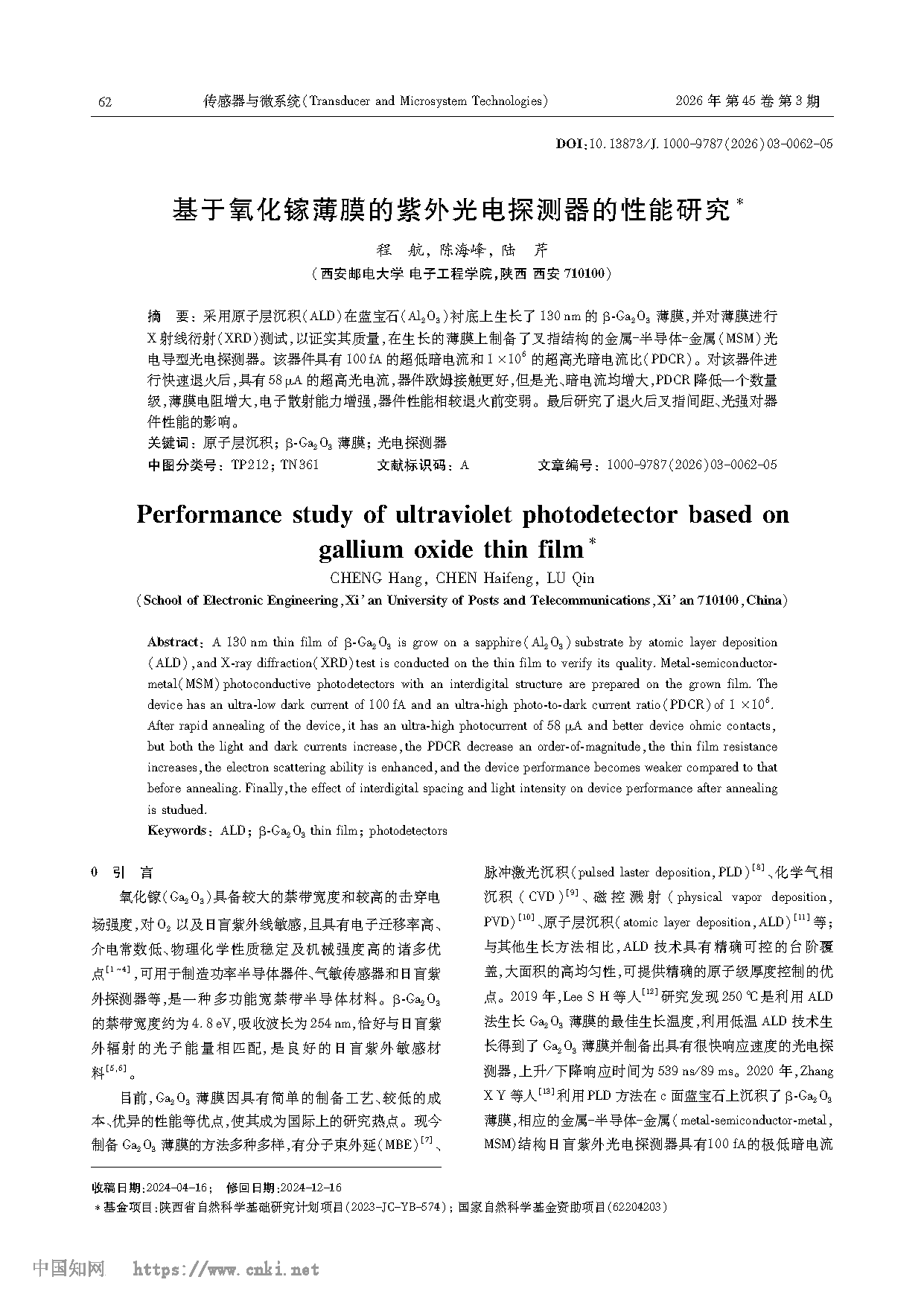
Fig.1 XRD pattern of Ga₂O₃ thin film
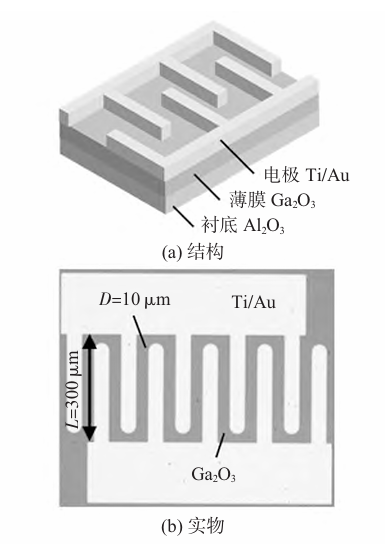
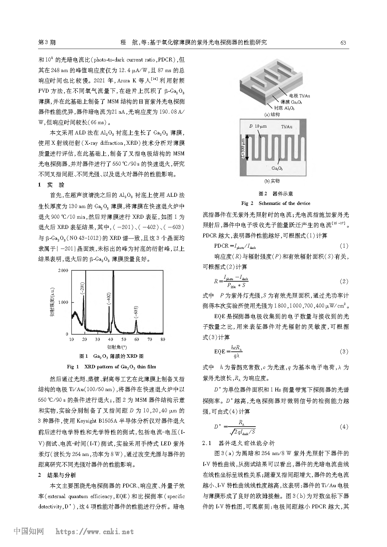
Fig.2 Schematic of the device
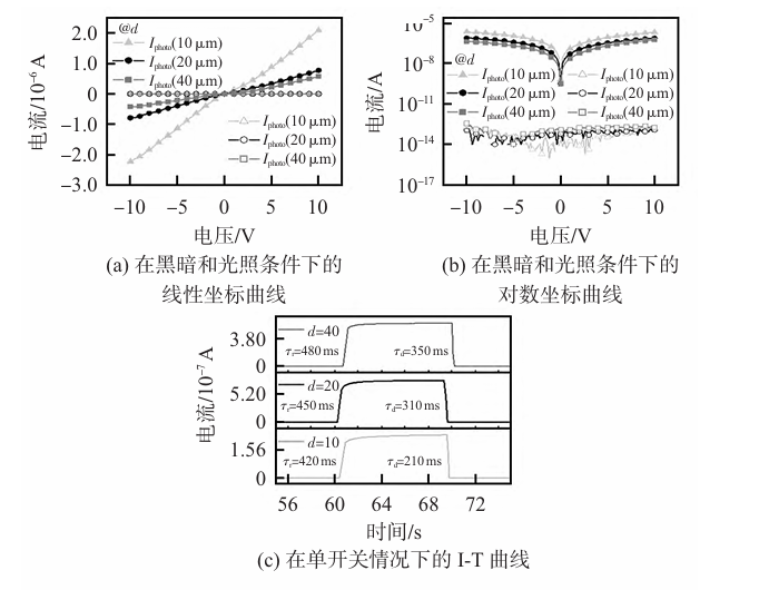
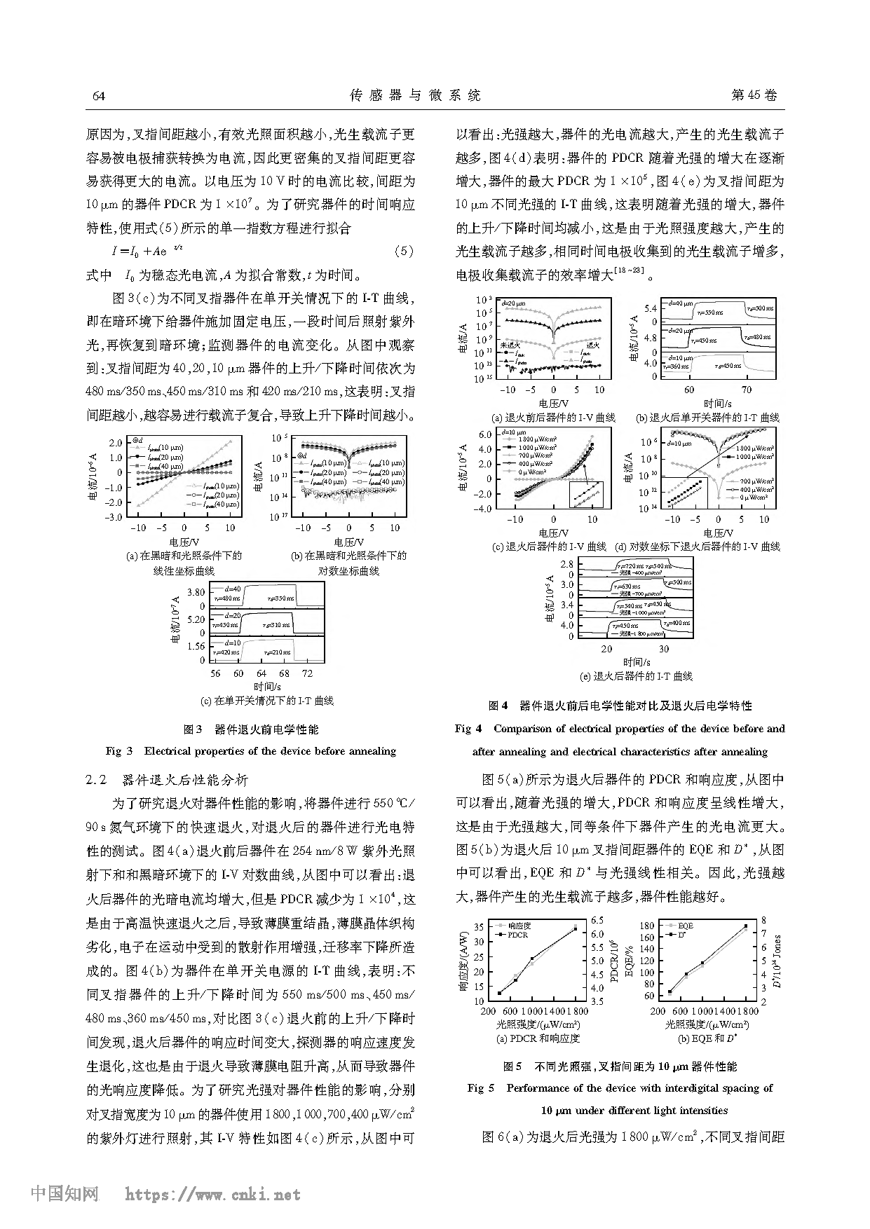
Fig.3 Electrical properties of the device before annealing
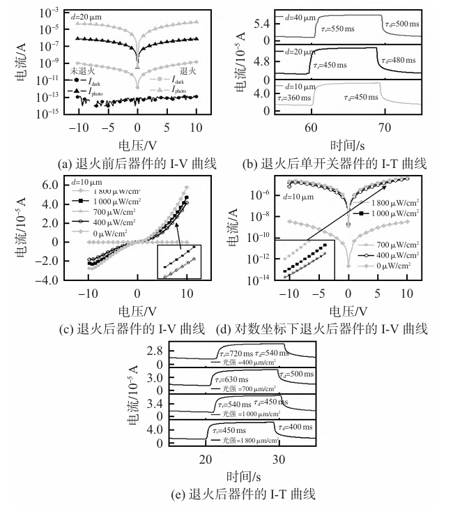
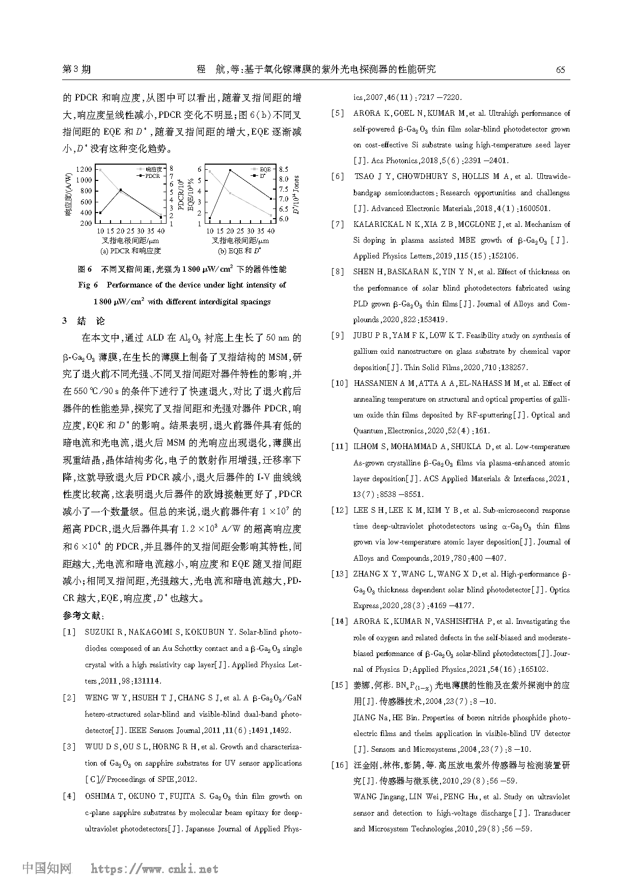
Fig.4 Comparison of electrical properties before and after annealing
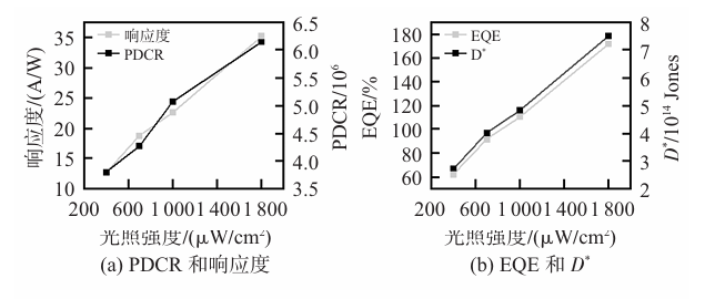
Fig.5 Device performance under different light intensities
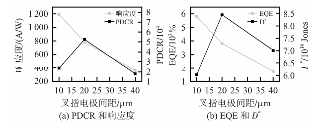
Fig.6 Device performance with different interdigital spacing
DOI:
10.13873/J.1000-9787(2026)03-0062-05