Paper Sharing
【Member Papers】Atomic-level revelation of spontaneous polarization orientation and piezoelectricity in ε-Ga₂O₃
日期:2026-04-10阅读:271
Researchers from Nanjing University of Posts and Telecommunications and The Hong Kong University of Science and Technology (Guangzhou) have published a dissertation titled "Atomic-level revelation of spontaneous polarization orientation and piezoelectricity in ε-Ga2O3" in Applied Physics Letters.
Background
Gallium oxide (Ga2O3) has emerged as a transformative material in power electronics, driven by its exceptional physical properties, including an ultrahigh critical breakdown field, superior Baliga’s figure of merit, and remarkable radiation hardness. Extensive research has focused on the thermodynamically stable β-Ga2O3, which has enabled significant advancements in high-voltage Schottky barrier diodes (SBDs), metal–oxide–semiconductor field effect transistors (MOSFETs), and heterojunction device architectures. However, recent investigations have highlighted the potential of the metastable ε-Ga2O3, which exhibits exceptional spontaneous polarization (Psp), substantial piezoelectric coefficients (d33), and a high dielectric constant (~32). These attributes position ε-Ga2O3 as a prime candidate for next-generation electronic systems, particularly in high electron mobility transistors (HEMTs) leveraging polarization-induced two-dimensional electron gas (2DEG) formation, low-loss radio frequency resonators exploiting piezoelectric coupling, and advanced gate dielectrics for semiconductor heterostructures.
Abstract
Advancing polarization control in semiconductors is pivotal for next-generation electronics, enabling revolutionary advances in energy and industrial systems. The metastable ε-Ga2O3 holds promise for polarization-engineered devices but remains hindered by unresolved polarization orientation and ambiguous piezoelectric responses. Here, using an integrated experimental and theoretical approach, we demonstrate that ε-Ga2O3 exhibits a spontaneous polarization (Psp)of 24.8 uC/cm2 oriented antiparallel to the crystal growth direction. The piezoelectric coefficient d33 was experimentally measured as 4.125 pm/V, in strong agreement with the theoretical value of 4.93 pm/V. The phase-pure ε-Ga2O3 films were grown via low-pressure mist-CVD with exceptional crystallinity, as evidenced by an x-ray diffractometer rocking curve [full-width-at-half-maximum (FWHM)=0.08]. Optimized piezoelectric force microscopy protocols were employed to determine d33, while the orientation of Psp was resolved using pulsed DC bias-dependent amplitude/phase-voltage measurements combined with aberration corrected scanning transmission electron microscopy. This multimodal methodology enabled direct mapping of bound charge distributions at the film surface and provided atomic-scale visualization of crystal orientation. These findings clarify ε-Ga2O3 polarization ambiguities, establish structure–property relationships, and unlock transformative potential for advancing power electronics, high-frequency communication systems, and energy-efficient memory technologies.
Conclusion
In conclusion, the ambiguity regarding both the orientation and magnitude of spontaneous polarization and piezoelectric properties in ε-Ga2O3 was resolved through a rigorously integrated experimental theoretical methodology. By synergizing LP-mist-CVD-grown epitaxial thin films with STEM, PFM, and theoretical analysis, we conclusively demonstrate that the intrinsic polarization vector in this polymorph is antiparallel to the crystal growth direction. Quantitative characterization reveals a spontaneous polarization of 24.8uC/cm2 and piezoelectric coefficients showing remarkable consistency between theory and experiment (d33=4.125pm/V from direct measurement vs 4.93pm/V from DFT calculations). These values not only establish fundamental structure–property relationships but also provide quantitative benchmarks for device design, particularly through PFM verified polarization mapping that demonstrates viable interfacial charge engineering for 2DEG formation. The combined results offer comprehensive validation of ε-Ga2O3’s dual-polarization mechanisms while reconciling previous theoretical predictions with experimental observations. To translate these insights into functional devices, future research may focus on optimizing growth processes to minimize sur face roughness, heterointerface engineering for charge confinement, and developing real-time polarization control strategies, thereby fully leveraging this material’s unique properties for power electronics and high-frequency devices.
Project Support
The work was supported by the C. K. Tan start-up fund from the Hong Kong University of Science and Technology (Guangzhou); the Guangzhou Municipal Science and Technology Project (Nos. 2023A03J0003, 2023A03J0013, 2023A04J0310, and 2023A03J0152); the Department of Education of Guangdong Province (No. 2024ZDZX1005); the State Administration of Foreign Experts Affairs (No. Y20240005); and the Shenzhen Science and Technology Innovation Commission (No. 20231115111658002).This work was supported by the Materials Characterization and Preparation Facility (MCPF) and Green Materials Laboratory at the Hong Kong University of Science and Technology (Guangzhou). The numerical calculations in this paper have been done using computational resources from Guangzhou Tanoxi Company.
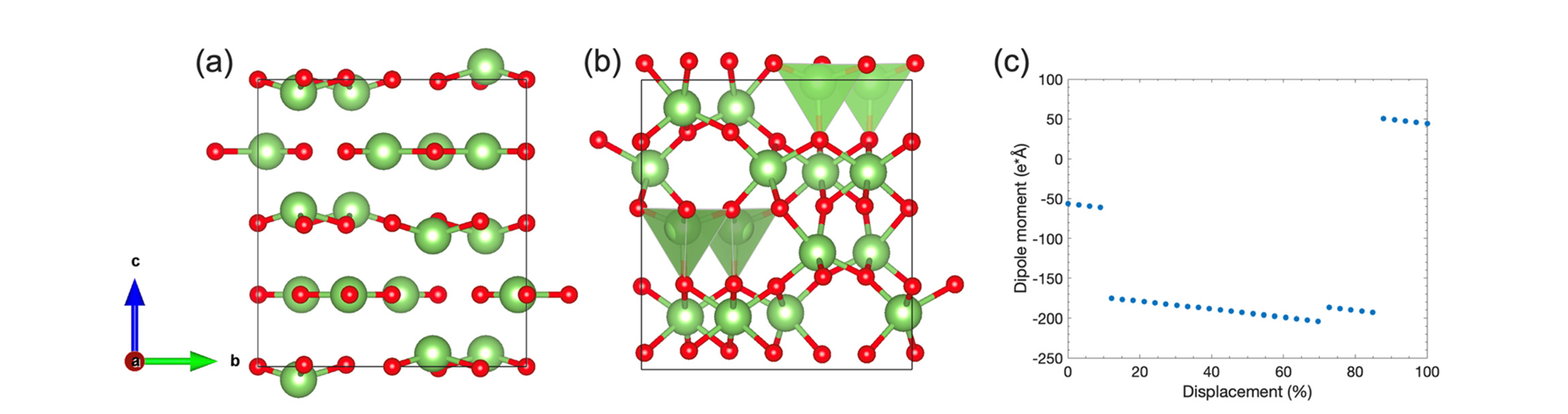
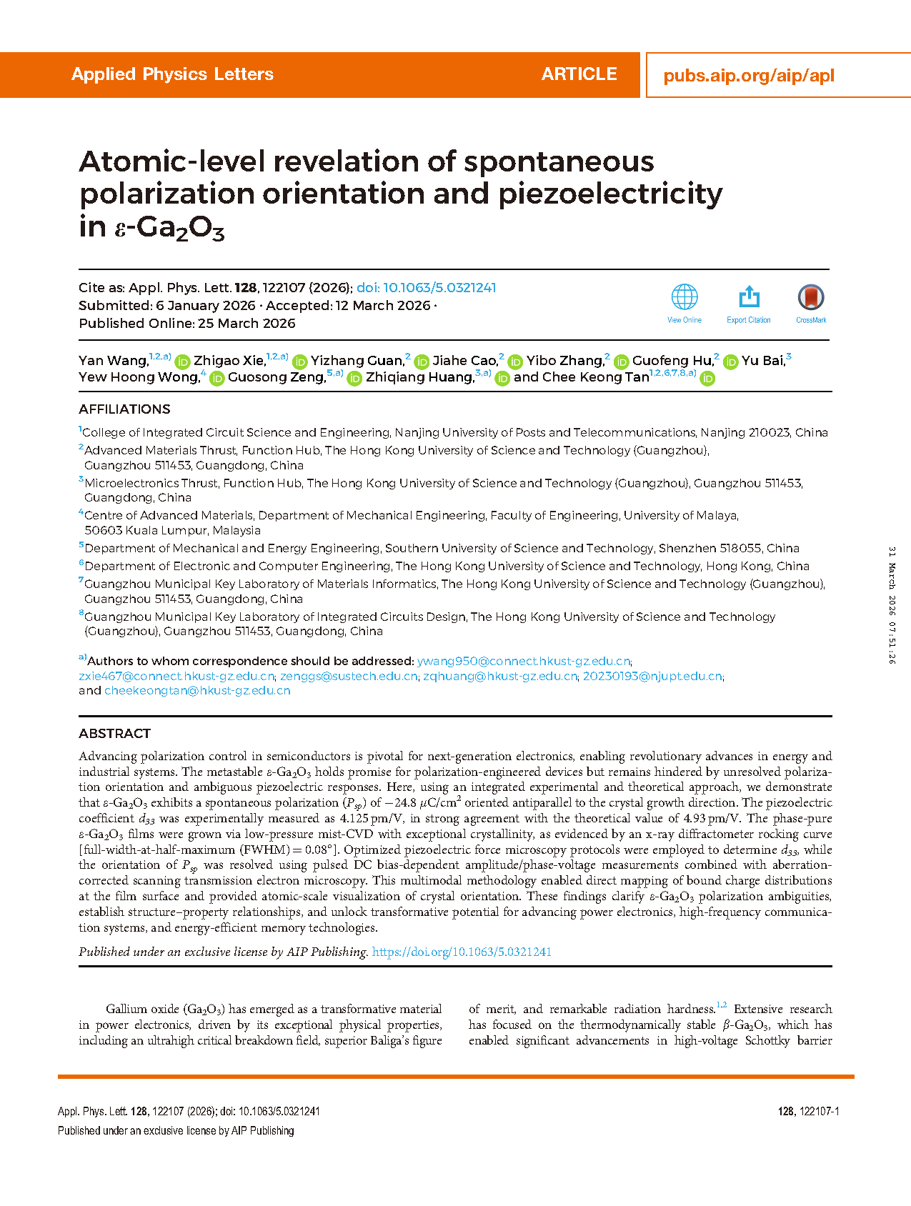
FIG. 1. (a) The centrosymmetric reference structure of ε-Ga2O3, with red spheres indicating oxygen atoms and green spheres indicating gallium atoms. (b) Polar structure of ε-Ga2O3. (c) Dipole moment of ε-Ga2O3 in different transition states.
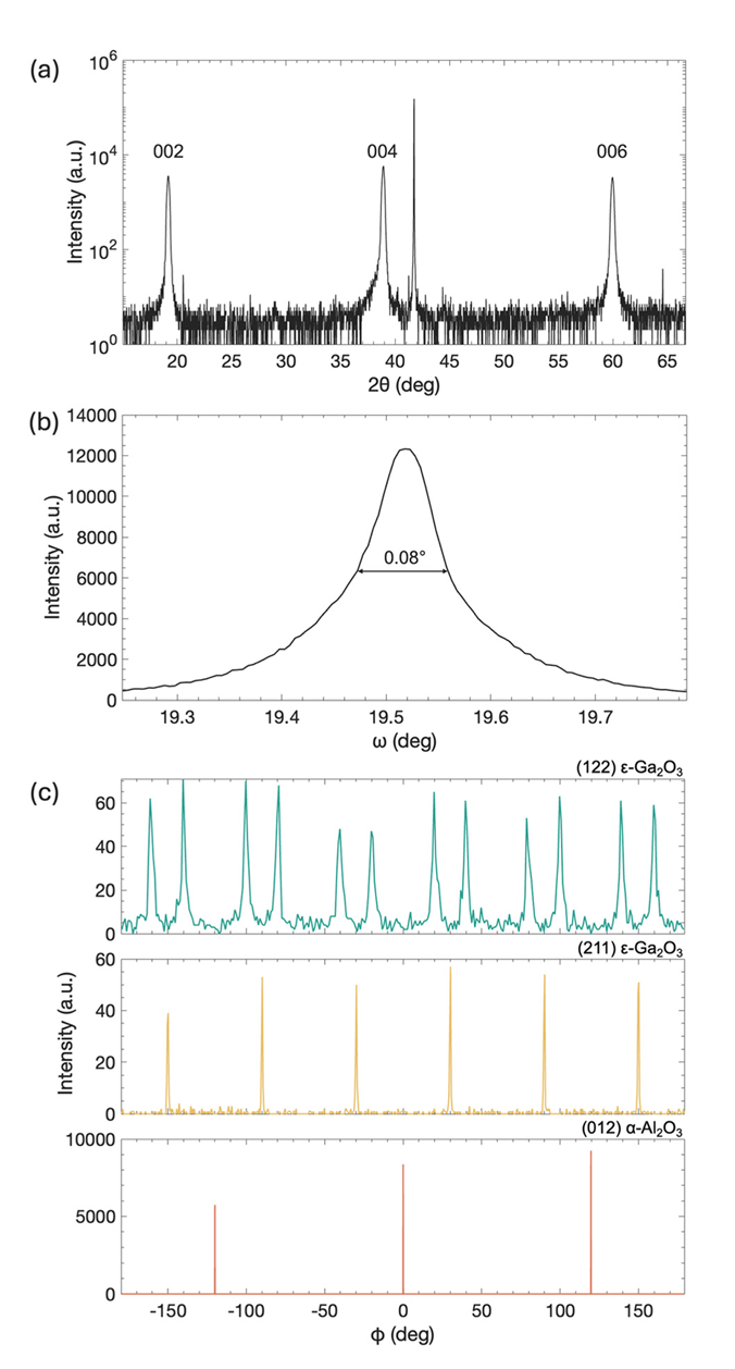
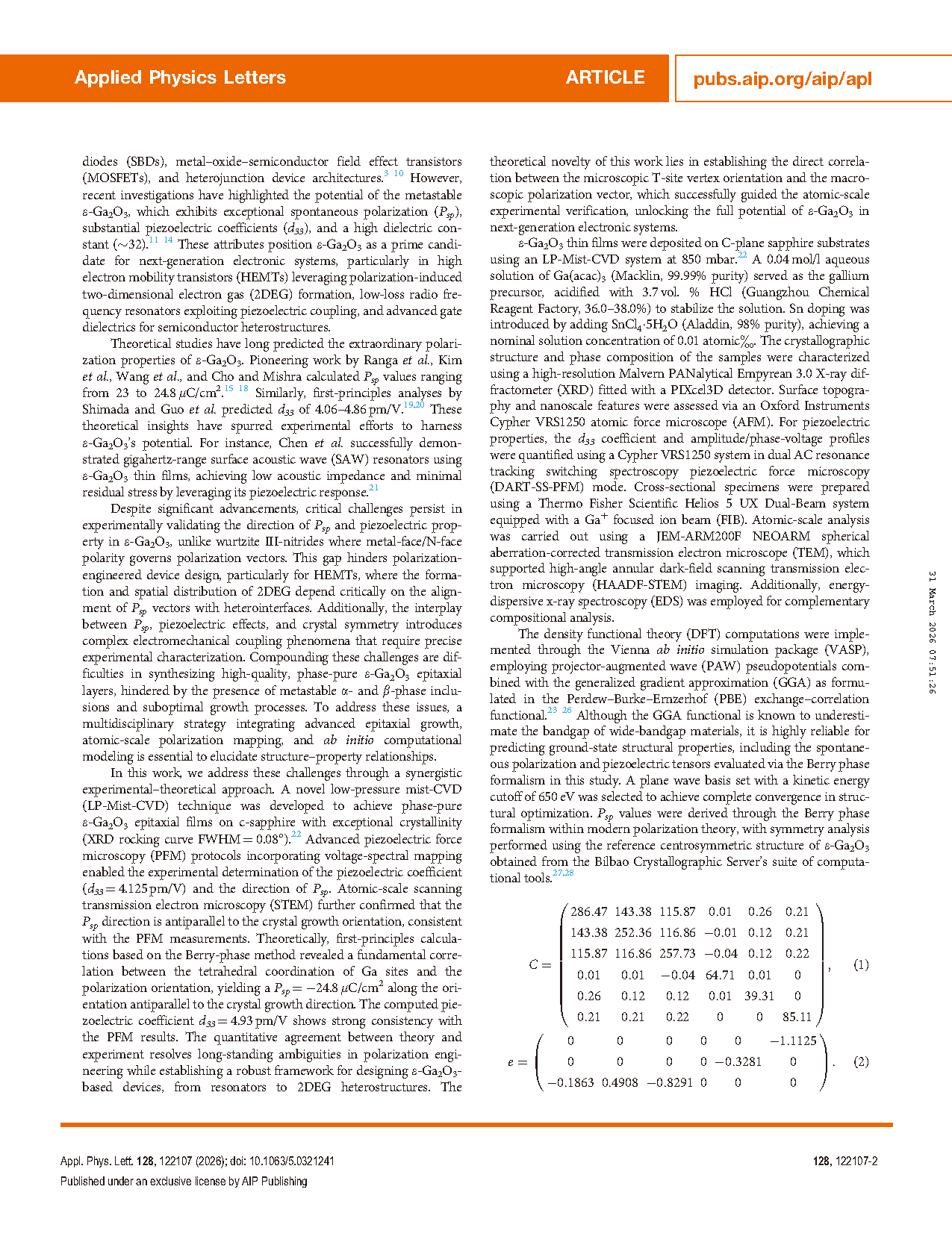
FIG. 2. (a) XRD 2h-scan profiles of ε-Ga2O3. (b) XRD rocking curves of the ε-Ga2O3 (004) reflection. (c) XRD u-scan for the (122), (211) plane of ε-Ga2O3 and the (012) plane of a-Al2O3.
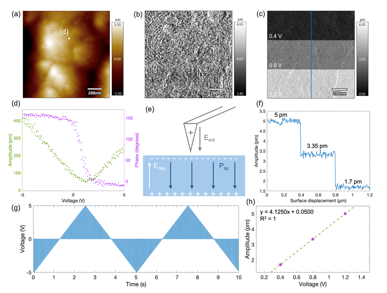
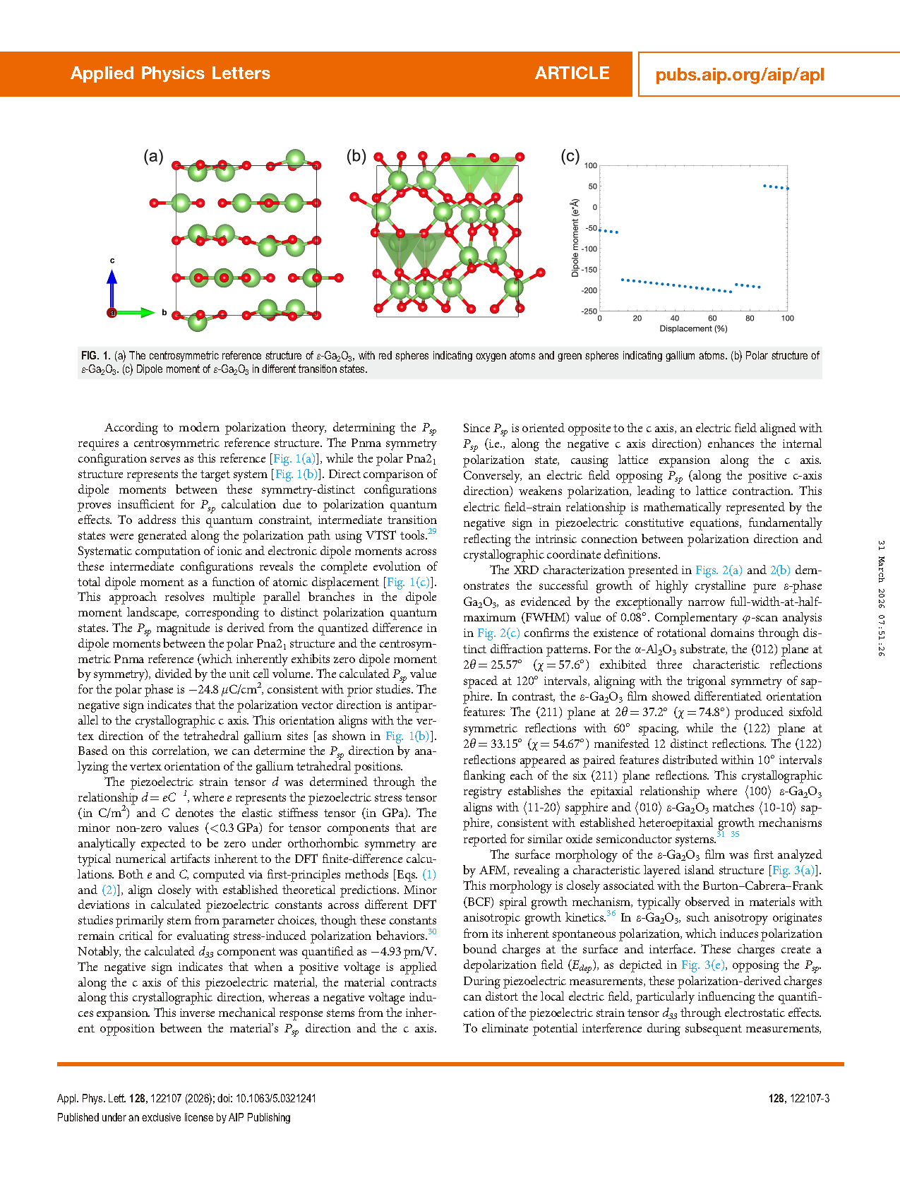
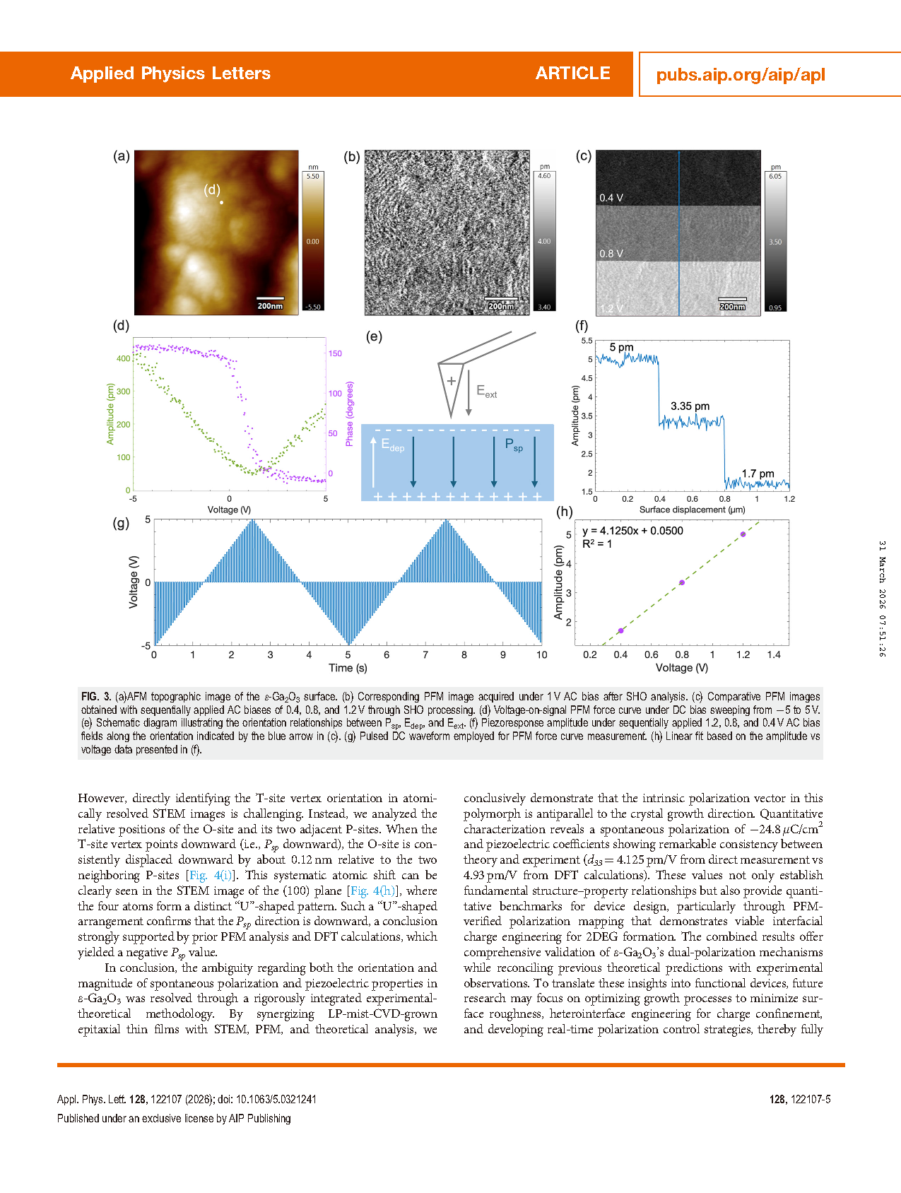
FIG. 3. (a)AFM topographic image of the ε-Ga2O3 surface. (b) Corresponding PFM image acquired under 1V AC bias after SHO analysis. (c) Comparative PFM images obtained with sequentially applied AC biases of 0.4, 0.8, and 1.2V through SHO processing. (d) Voltage-on-signal PFM force curve under DC bias sweeping from 5 to 5V. (e) Schematic diagram illustrating the orientation relationships between Psp,Edep, and Eext. (f) Piezoresponse amplitude under sequentially applied 1.2, 0.8, and 0.4 V AC bias fields along the orientation indicated by the blue arrow in (c). (g) Pulsed DC waveform employed for PFM force curve measurement. (h) Linear fit based on the amplitude vs voltage data presented in (f).
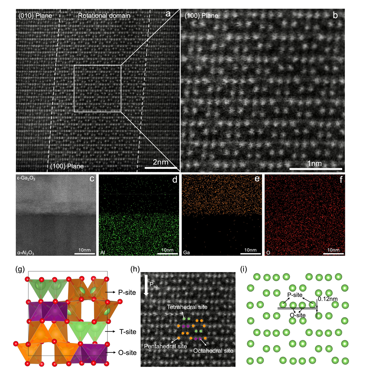
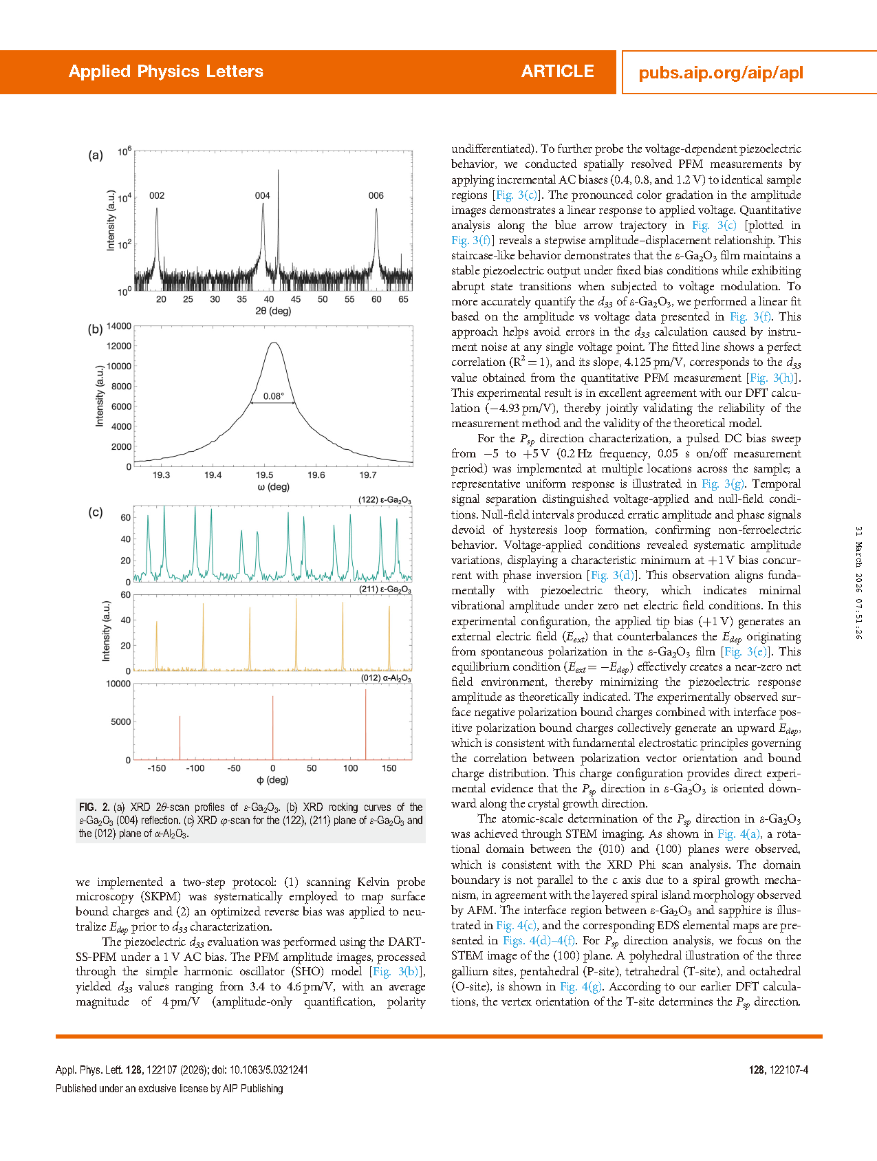
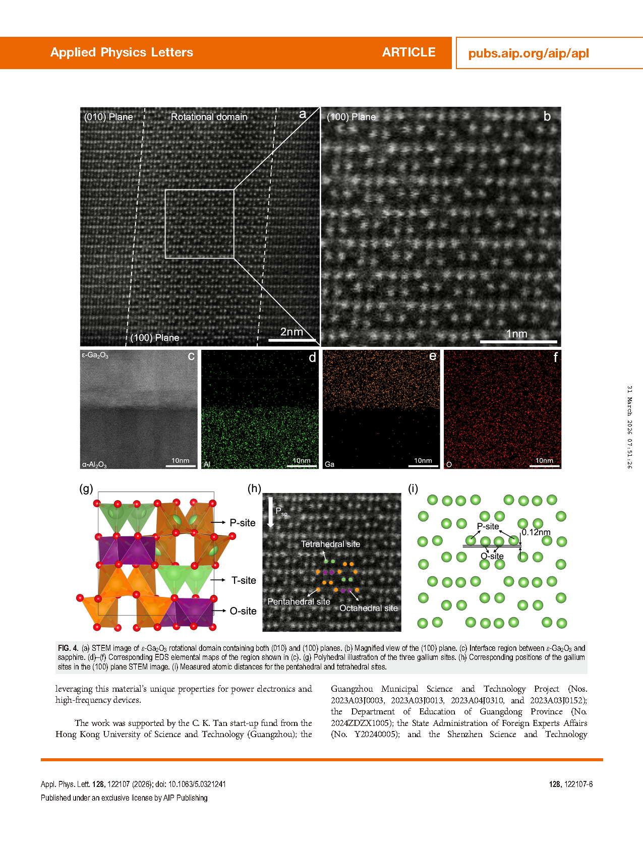
FIG. 4. (a) STEM image of ε-Ga2O3 rotational domain containing both (010) and (100) planes. (b) Magnified view of the (100) plane. (c) Interface region between ε-Ga2O3 and sapphire. (d)–(f) Corresponding EDS elemental maps of the region shown in (c). (g) Polyhedral illustration of the three gallium sites. (h) Corresponding positions of the gallium sites in the (100) plane STEM image. (i) Measured atomic distances for the pentahedral and tetrahedral sites.
DOI:
doi.org/10.1063/5.0321241