


Member Intro
【Member Intro】Suzhou Institute of Nano-Tech and Nano-Bionics(SINANO),Chinese Academy of Science —— Regular Member
日期:2023-04-21阅读:1107
Profile
Suzhou Institute of Nanotechnology and Nanobionics(SINANO), Chinese Academy of Sciences, was jointly founded in 2006 by the Chinese Academy of Sciences, the People's Government of Jiangsu Province, the People's Government of Suzhou City and Suzhou Industrial Park. It is located in the beautiful Dushu Lake Science and Education Innovation Zone of Suzhou Industrial Park.

SINANO has laid out key research fields such as electronic information, biomedicine, and functional materials in a forward-looking manner, integrating advantageous forces and refining disciplinary directions. It actively undertakes major national scientific and technological tasks, and carries out cutting-edge scientific research and key core technology in related fields. It has establishes a scientific and technological innovation team that includes academicians, national elites, and other key national talents, producing a batch of original scientific and technological achievements, independently developing a series of instruments and equipment. It has formed a research system with its own characteristics, and strove to become a national strategic scientific and technological force in the field of nanotechnology.
Science and technology infrastructure is the cornerstone of SINANO. Focusing on key fields, SINANO has built four public technology platforms integrating scientific research and public service --- nanometer processing platform, test and analysis platform, biochemical platform, nano vacuum interconnection experimental station, with strong ability to support major national scientific research tasks, serving scientific research and product development. The Institute has formed common technologies, focusing on original equipment research and development, to promote regional industrial agglomeration and development, and to strengthen the transformation of technological innovation resources, and provide strong support for the development of nanotechnology and related industries.
The Nano Processing Platform of the Institute is a member of the National Micro Nano Processing and Manufacturing Industry Technology Innovation Strategic Alliance, Nano Device Platform of the Chinese Academy of Sciences, the Jiangsu Province Nano Processing Public Service Platform, the Suzhou Micro Nano Device Processing and System Integration Public Service Platform, the Suzhou Micro Nano Processing Training Base, and the Suzhou Industrial Park Nano Technology Talent Training Base. The disciplinary research of the platform covers the fields including the growth, process development, power device development of new wide bandgap semiconductor materials such as gallium oxide, gallium nitride, and silicon carbide. The research also covers spintronics, nano optical/electronic devices for two-dimensional material heterojunctions, photonic chips, and advanced microelectromechanical systems and integration.
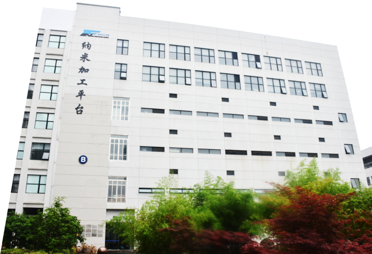
Nano Processing Platform is a public open platform integrating semiconductor micro/nano processing, detection and packaging, with advanced equipment and characteristic services. With over 10000 square meters of ultra clean laboratories and over 300 sets of large-scale equipment, the platform has the ability to conduct scientific research and product development on micro and nano electronic devices, micro electromechanical systems, optoelectronic devices, power devices, and biochips. The platform provides technical consultation, customized micro/nano processing services, and professional training for micro/nano processing to a large number of customers, enabling equipment to be shared and allowing users to operate independently and conduct independent research and development. At the same time, the platform has also established an innovative cooperation model that integrates "production, learning, research, and inspection" to jointly tackle key issues with enterprises and universities, assisting the development of the national semiconductor industry and creating a first-class micro/nano processing research and development and service base in the world.

