Paper Sharing
【Domestic Papers】Mixed-dimensional gallium oxide/two-dimensional material heterostructures for advanced electronics and optoelectronics
日期:2026-04-13阅读:197
Researchers from Beijing Institute of Technology have published a dissertation titled " Mixed-dimensional gallium oxide/two-dimensional material heterostructures for advanced electronics and optoelectronics " in Journal of Materials Chemistry C.
Background
With the increasing demand for computing power in modern artificial intelligence technology, the implementation of key functionalities in emerging computing architectures is highly dependent on silicon complementary metal–oxide-semiconductor(CMOS) electronics. Field-effect transistors (FETs), as the fundamental core components of modern computer processors, control the development of integrated circuits (ICs). Metal oxide-semiconductor field-effect transistors (MOSFETs) have become the foundation of modern electronics due to their high efficiency, fast switching speed, and low power consumption. However, with the development of high-density integrated cir cuits, the integration of Si CMOS devices is limited by size reduction. One way to scaling CMOS technology is to use high-k dielectric materials instead of SiO2, such as Ga2O3 and HfO2. Ga2O3, as a new generation semiconductor material, is widely used in fields such as light-emitting diodes, photodetec tors, MOSFETs, etc. due to its wide bandgap, high breakdown field strength, and excellent carrier mobility, highlighting its enormous potential for application in advanced optoelectronic devices. There have been various synthesis methods, such as magnetron sputtering, pulsed laser deposition (PLD), molecular beam epitaxy (MBE), etc.
Abstract
In the current era of big data, it is crucial to develop advanced optoelectronic devices that integrate sensing, storage, computing, and other functions to meet the diverse needs of information processing systems for high energy efficiency, high performance, and emerging functions of electronic devices. Gallium oxide (Ga2O3) stands out in fields such as photodetectors, field effect transistors, and gas sensors due to its advantages of ultra-wide bandgap (4.8–5.4 eV), high breakdown field strength (8 MV cm-1) and high dielec tric constant, becoming the preferred material for the next generation of high-power devices. To overcome the size limitation of transistor performance in the Moore era, two-dimensional (2D) materials have received widespread attention in the field of electronic devices due to their advantages such as atomic thickness, no dangling bonds, and large specific surface area. Here, we provide a comprehensive review of the growth, integration and application of Ga2O3/2D heterojunctions in optoelectronic devices. This review summarizes their innovative applications in logic functional transistors, ultraviolet detectors, memory storage, optoelectronic synapse devices and flexible electronic devices, aiming to promote the practical application of Ga2O3-based devices and provide new ideas for the development of multifunctional integrated devices.
Conclusion
In summary, the development of devices based on Ga2O3/2D heterostructures is expected to address the limitations of Si based technology. With deep cooperation in multiple fields such as materials science, micro/nano processing, and compu tational science, it will promote the development of the next generation of high-efficiency, multifunctional integrated elec tronic systems.
Project Support
The authors acknowledge support from the National Key Research and Development Program of China (Grant No. 2023YFB3208002), the Analysis & Testing Center of Beijing Institute of Technology, the start-up fund of Beijing Institute of Technology, and the Fundamental and Interdisciplinary Disciplines Breakthrough Plan of the Ministry of Education of China.
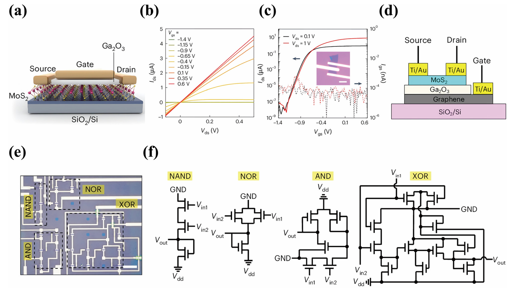
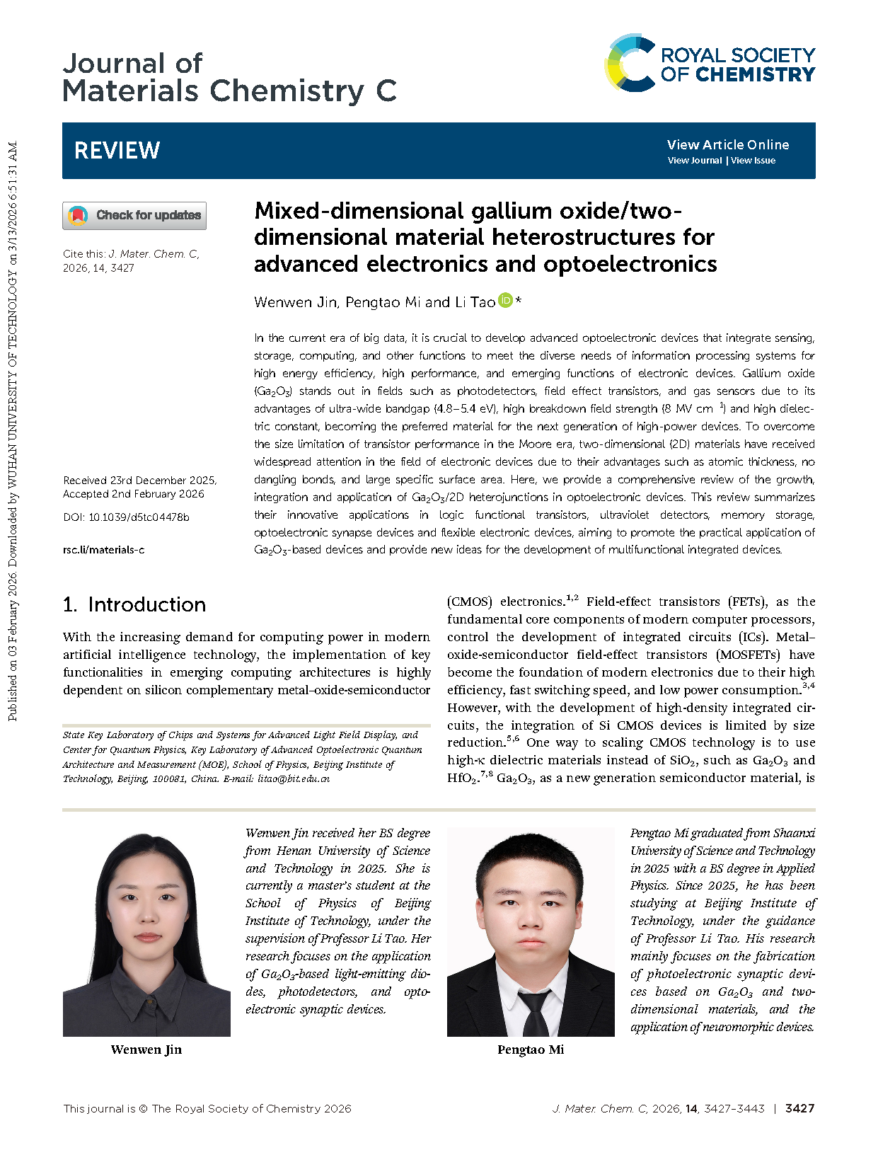
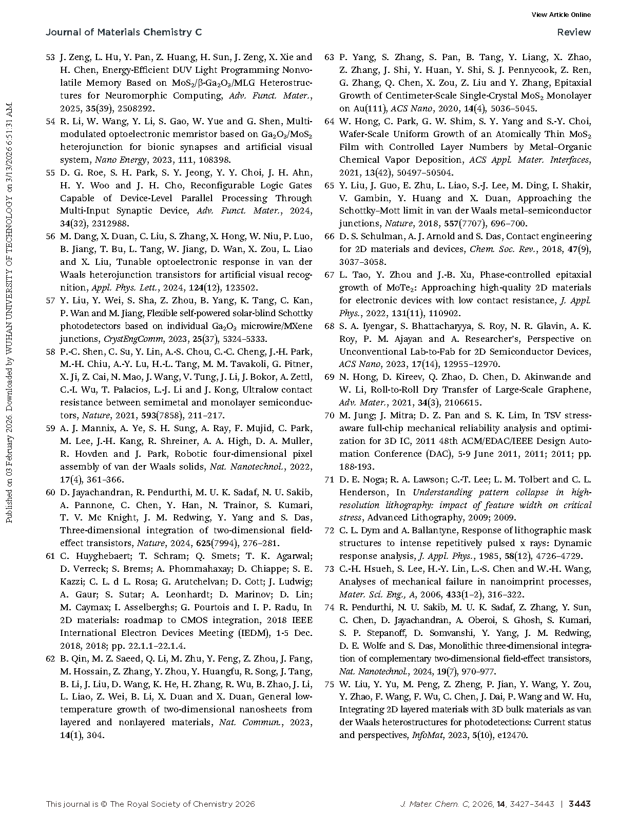
Fig. 1 (a) Schematic illustration of the Ga2O3/MoS2 FET. (b) Output curves of the top-gated FETs when the gate voltage ranges from 1.4 to 0.6 V. (c) Transfer curves of the top-gated FETs when the Vds is 0.1 and 1 V. Inset: optical microscopy image of the corresponding FET. (d) Schematic illustration of the bottom-gated FETs. (e) Optical microscopy image of the logic gates. (f) Equivalent circuit diagrams of NAND, NOR, AND and XOR gates. Reproduced with permission from ref. 47.
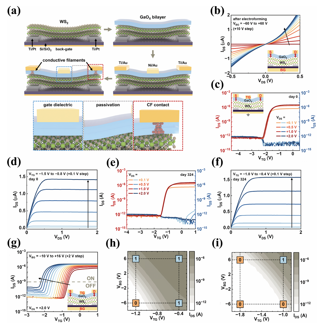
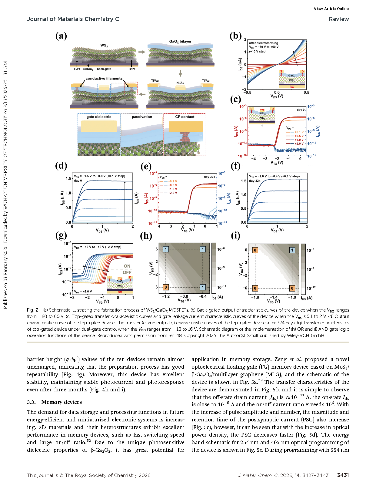
Fig. 2 (a) Schematic illustrating the fabrication process of WS2/GaOX MOSFETs. (b) Back-gated output characteristic curves of the device when the VBG ranges from -60 to 60 V. (c) Top-gated transfer characteristic curves and gate leakage current characteristic curves of the device when the Vds is 0.1 to 2 V. (d) Output characteristic curve of the top-gated device. The transfer (e) and output (f) characteristic curves of the top-gated device after 324 days. (g) Transfer characteristics of top-gated device under dual-gate control when the VBG ranges from 10 to 16 V. Schematic diagram of the implementation of (h) OR and (i) AND gate logic operation functions of the device.
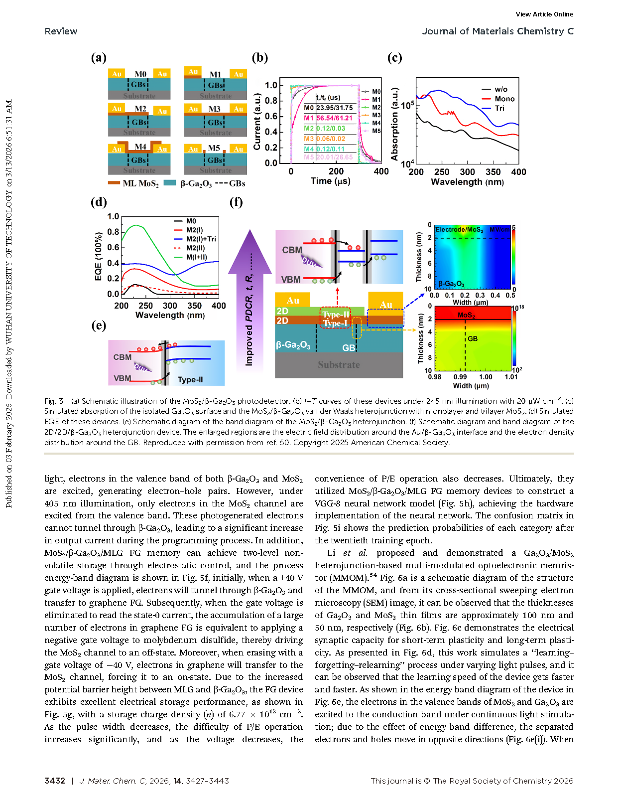
Fig. 3 (a) Schematic illustration of the MoS2/b-Ga2O3 photodetector. (b) I–T curves of these devices under 245 nm illumination with 20 uW cm-2. (c) Simulated absorption of the isolated Ga2O3 surface and the MoS2/b-Ga2O3 van der Waals heterojunction with monolayer and trilayer MoS2. (d) Simulated EQE of these devices. (e) Schematic diagram of the band diagram of the MoS2/b-Ga2O3 heterojunction. (f) Schematic diagram and band diagram of the 2D/2D/b-Ga2O3 heterojunction device. The enlarged regions are the electric field distribution around the Au/b-Ga2O3 interface and the electron density distribution around the GB.
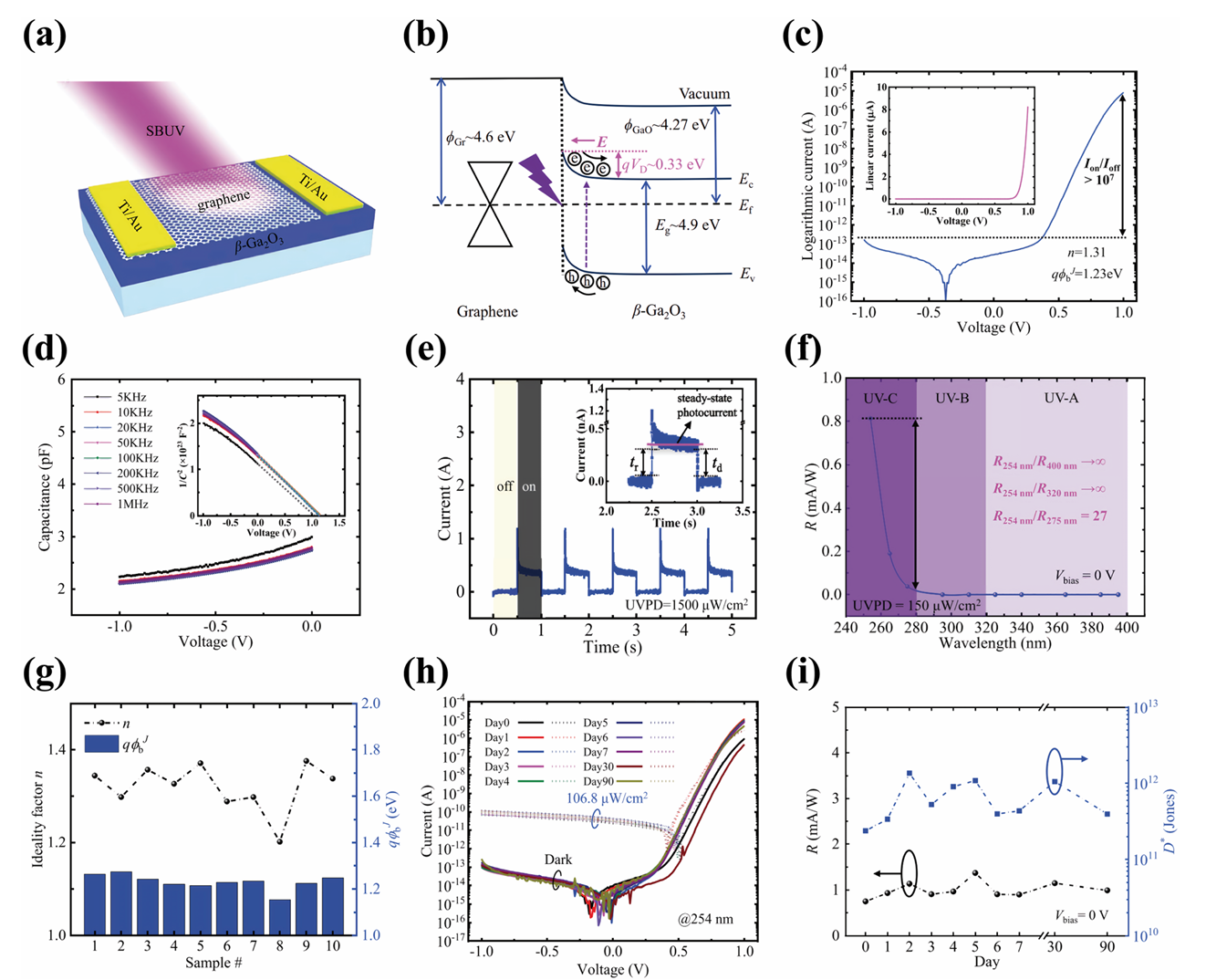
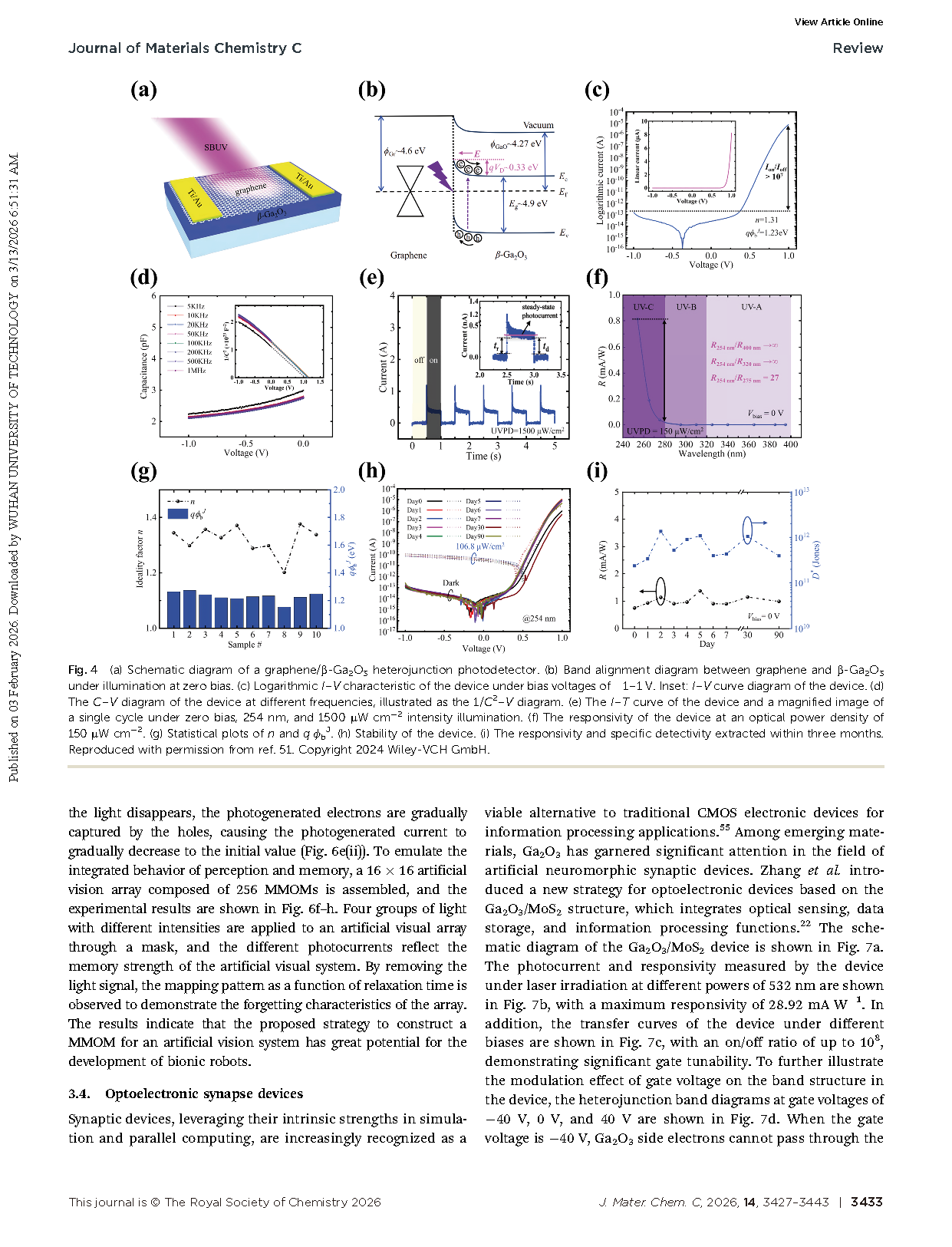
Fig. 4 (a) Schematic diagram of a graphene/b-Ga2O3 heterojunction photodetector. (b) Band alignment diagram between graphene and b-Ga2O3 under illumination at zero bias. (c) Logarithmic I–V characteristic of the device under bias voltages of 1–1 V. Inset: I–V curve diagram of the device. (d) The C–V diagram of the device at different frequencies, illustrated as the 1/C2–V diagram. (e) The I–T curve of the device and a magnified image of a single cycle under zero bias, 254 nm, and 1500 uW cm-2 intensity illumination. (f) The responsivity of the device at an optical power density of 150 uW cm-2. (g) Statistical plots of n. (h) Stability of the device. (i) The responsivity and specific detectivity extracted within three months.
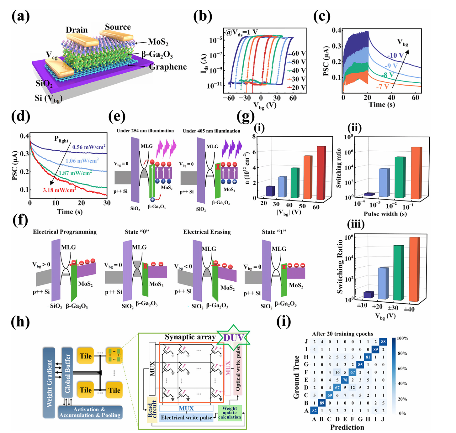
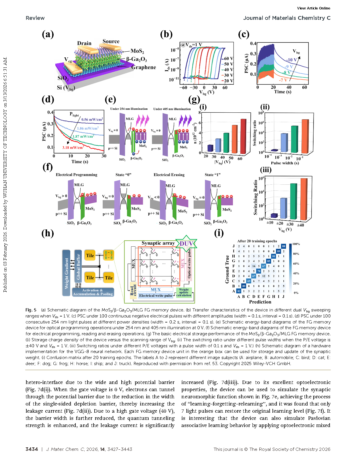
Fig. 5 (a) Schematic diagram of the MoS2/b-Ga2O3/MLG FG memory device. (b) Transfer characteristics of the device in different dual Vbg sweeping ranges when Vds=1V.(c) PSC under 100continuous negative electrical pulses with different amplitudes (width = 0.1 s, interval = 0.1 s). (d) PSC under 100 consecutive 254 nm light pulses at different power densities (width = 0.2 s, interval = 0.1 s). (e) Schematic energy-band diagrams of the FG memory device for optical programming operations under 254 nm and 405 nm illumination at 0 V. (f) Schematic energy-band diagrams of the FG memory device for electrical programming, reading and erasing operations. (g) The basic electrical storage performance of the MoS2/b-Ga2O3/MLG FG memory device. ((i) Storage charge density of the device versus the scanning range of Vbg. (ii) The switching ratio under different pulse widths when the P/E voltage is ± 40 V and Vds = 1 V. (iii) Switching ratios under different P/E voltages with a pulse width of 0.1 s and Vds = 1 V.) (h) Schematic diagram of a hardware implementation for the VGG-8 neural network. Each FG memory device unit in the orange box can be used for storage and update of the synaptic weight. (i) Confusion matrix after 20 training epochs. The labels A to J represent different image subjects (A: airplane; B: automobile; C: bird; D: cat;E: deer; F: dog; G: frog; H: horse; I: ship; and J: truck).
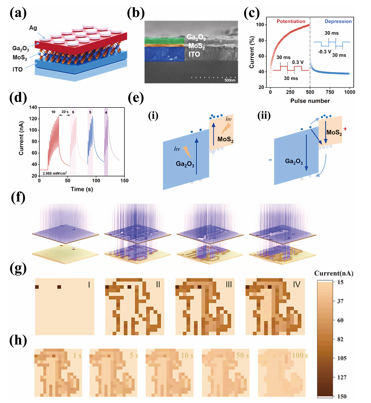
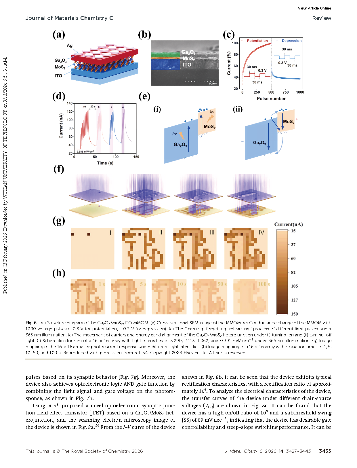
Fig. 6 (a) Structure diagram of the Ga2O3/MoS2/ITO MMOM. (b) Cross-sectional SEM image of the MMOM. (c) Conductance change of the MMOM with 1000 voltage pulses (+0.3 V for potentiation, 0.3 V for depression). (d) The ‘‘learning–forgetting–relearning’ process of different light pulses under 365 nmillumination. (e) The movement of carriers and energy band alignment of the Ga2O3/MoS2 heterojunction under (i) turning-on and (ii) turning-off light. (f) Schematic diagram of a 16 × 16 array with light intensities of 3.290, 2.113, 1.052, and 0.391 mW cm-2 under 365 nm illumination. (g) Image mapping of the 16 16arrayforphotocurrentresponse under different light intensities. (h) Image mapping of a 16 16 array with relaxation times of 1, 5, 10, 50, and 100 s.
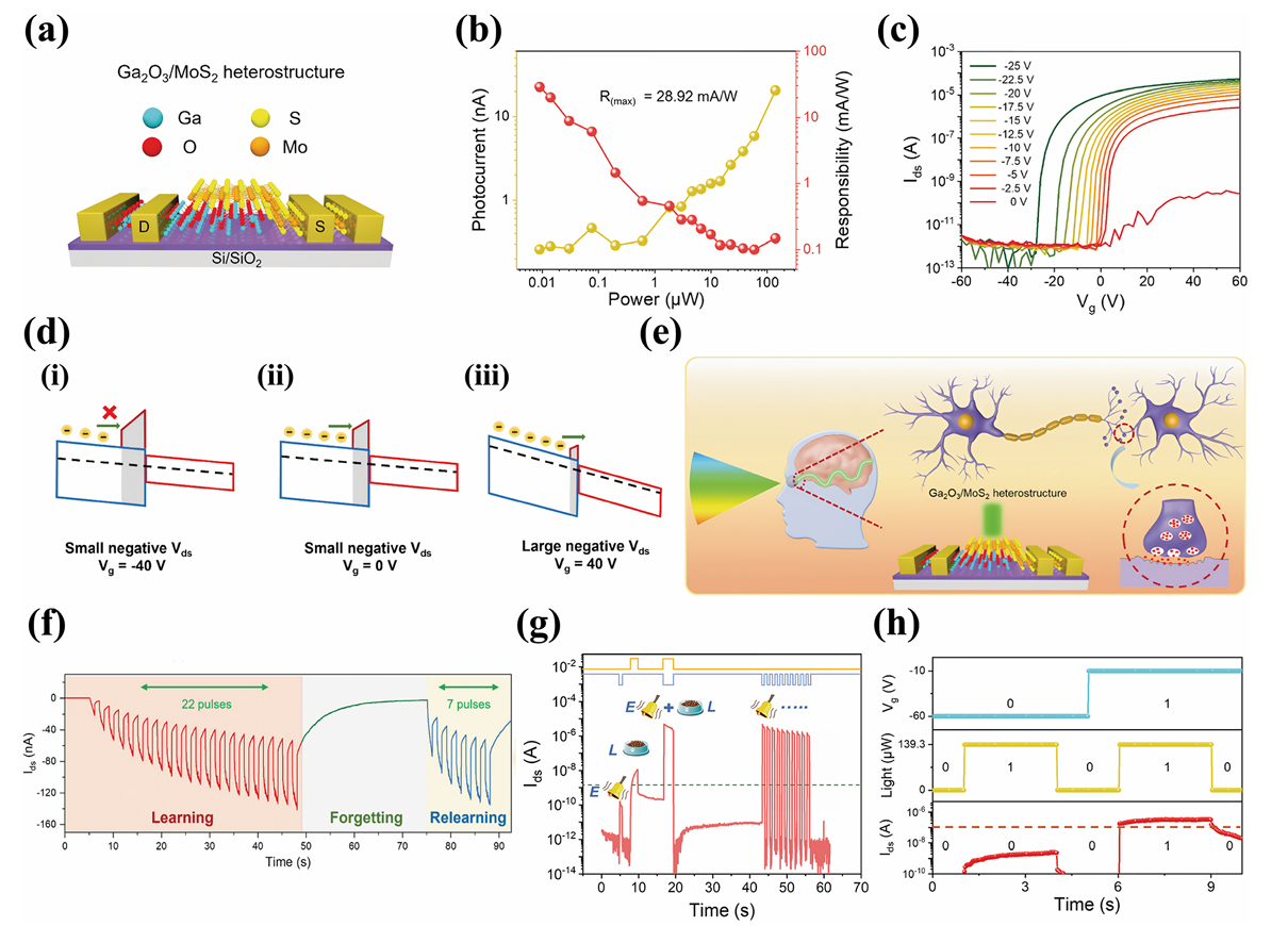
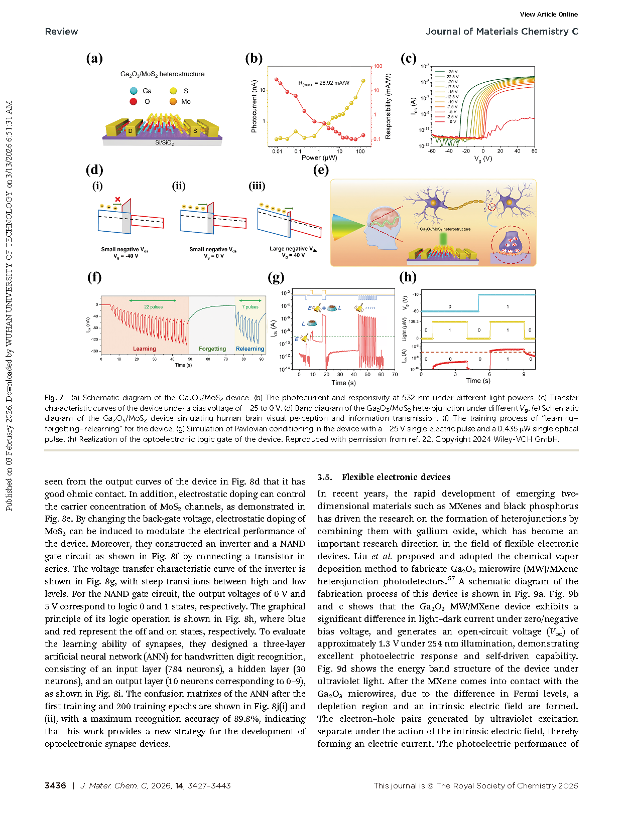
Fig. 7 (a) Schematic diagram of the Ga2O3/MoS2 device. (b) The photocurrent and responsivity at 532 nm under different light powers. (c) Transfer characteristic curves of the device under a bias voltage of 25 to 0 V.(d) Band diagram oftheGa2O3/MoS2 heterojunction under different Vg. (e)Schematic diagram of the Ga2O3/MoS2 device simulating human brain visual perception and information transmission. (f) The training process of “learning-forgetting-relearning” for the device. (g) Simulation of Pavlovian conditioning in the device with a 25 V single electric pulse and a 0.435 uW single optical pulse. (h) Realization of the optoelectronic logic gate of the device.
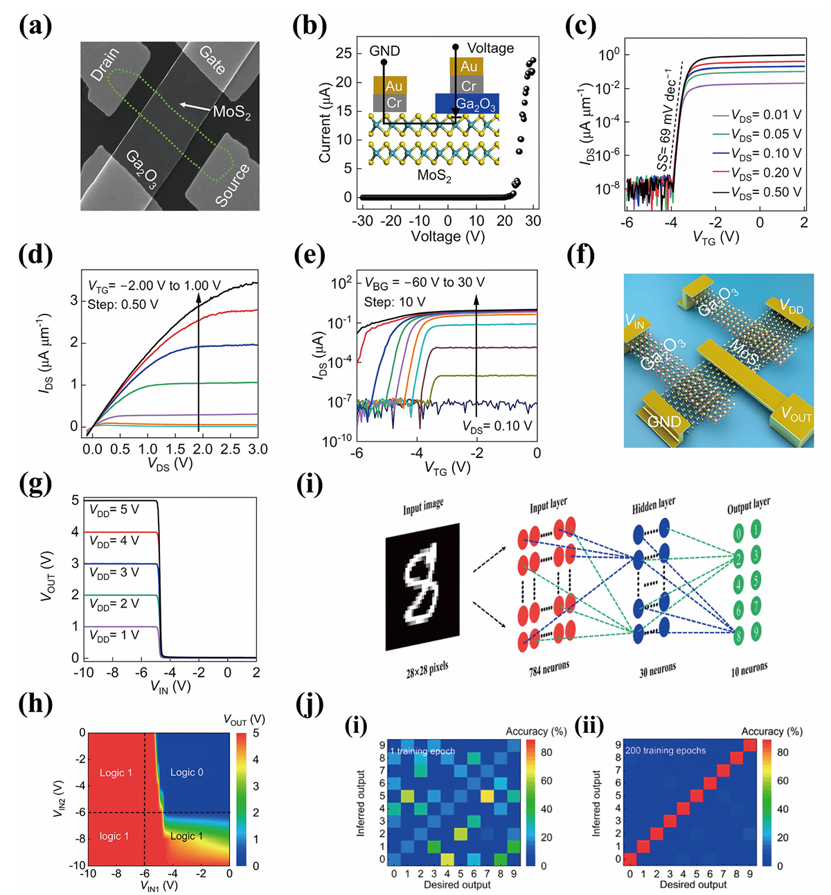
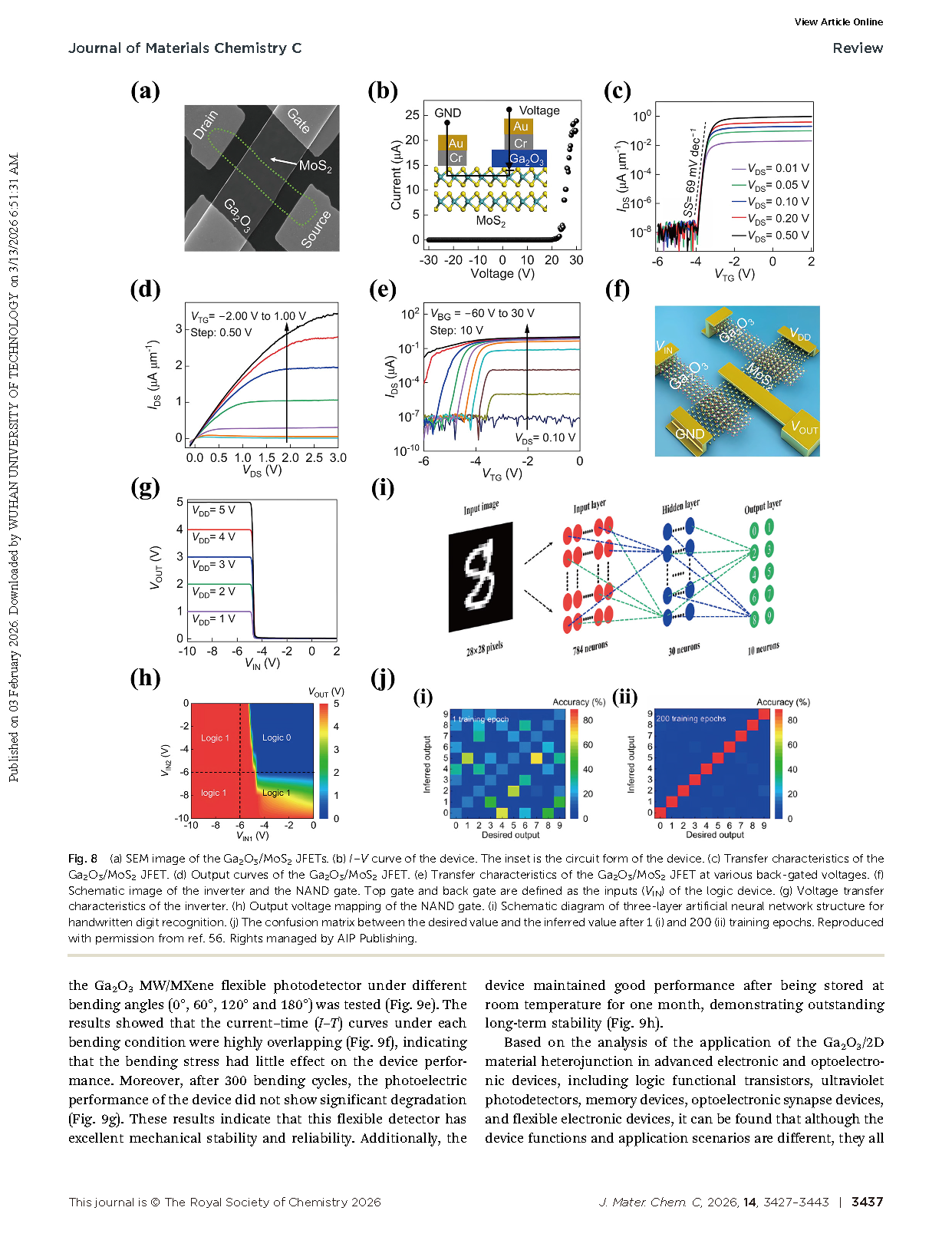
Fig. 8 (a) SEM image of the Ga2O3/MoS2 JFETs. (b) I–V curve of the device. The inset is the circuit form of the device. (c) Transfer characteristics of the Ga2O3/MoS2 JFET. (d) Output curves of the Ga2O3/MoS2 JFET. (e) Transfer characteristics of the Ga2O3/MoS2 JFET at various back-gated voltages. (f) Schematic image of the inverter and the NAND gate. Top gate and back gate are defined as the inputs (VIN) of the logic device. (g) Voltage transfer characteristics of the inverter. (h) Output voltage mapping of the NAND gate. (i) Schematic diagram of three-layer artificial neural network structure for handwritten digit recognition. (j) The confusion matrix between the desired value and the inferred value after 1 (i) and 200 (ii) training epochs.
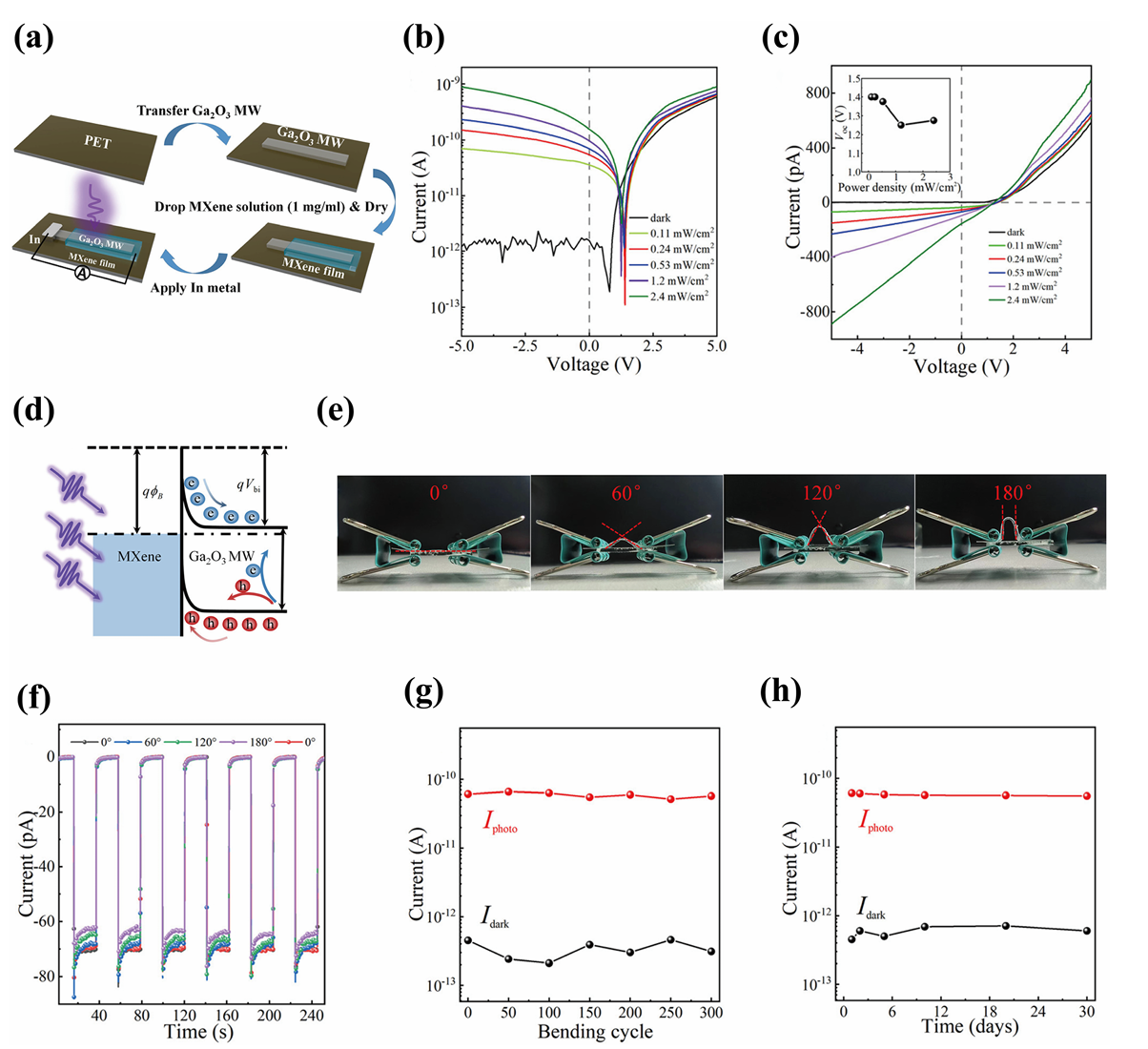
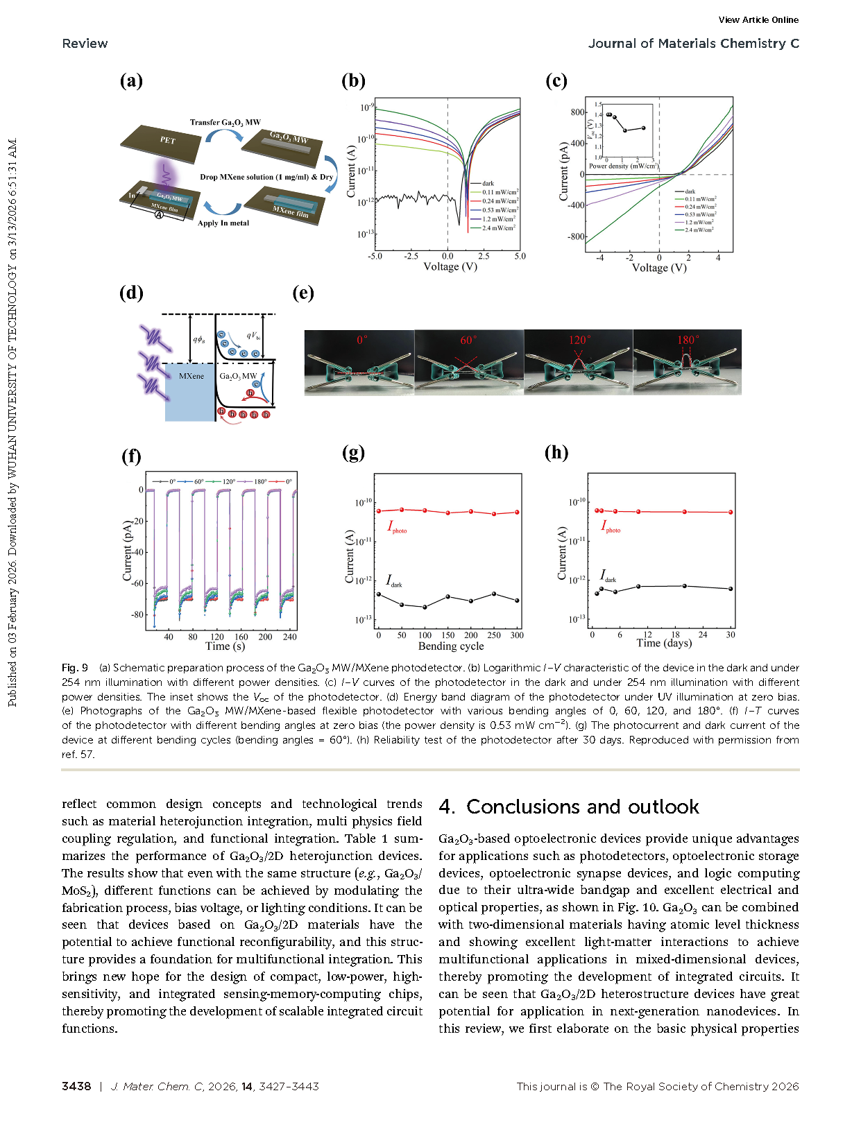
Fig. 9 (a) Schematic preparation process of the Ga2O3 MW/MXene photodetector. (b) Logarithmic I–V characteristic of the device in the dark and under 254 nm illumination with different power densities. (c) I–V curves of the photodetector in the dark and under 254 nm illumination with different power densities. The inset shows the Voc of the photodetector. (d) Energy band diagram of the photodetector under UV illumination at zero bias. (e) Photographs of the Ga2O3 MW/MXene-based flexible photodetector with various bending angles of 0, 60, 120, and 1801. (f) I–T curves of the photodetector with different bending angles at zero bias (the power density is 0.53 mW cm-2). (g) The photocurrent and dark current of the device at different bending cycles (bending angles = 601). (h) Reliability test of the photodetector after 30 days.
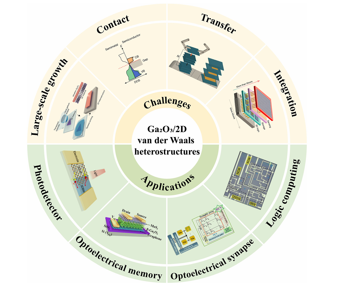
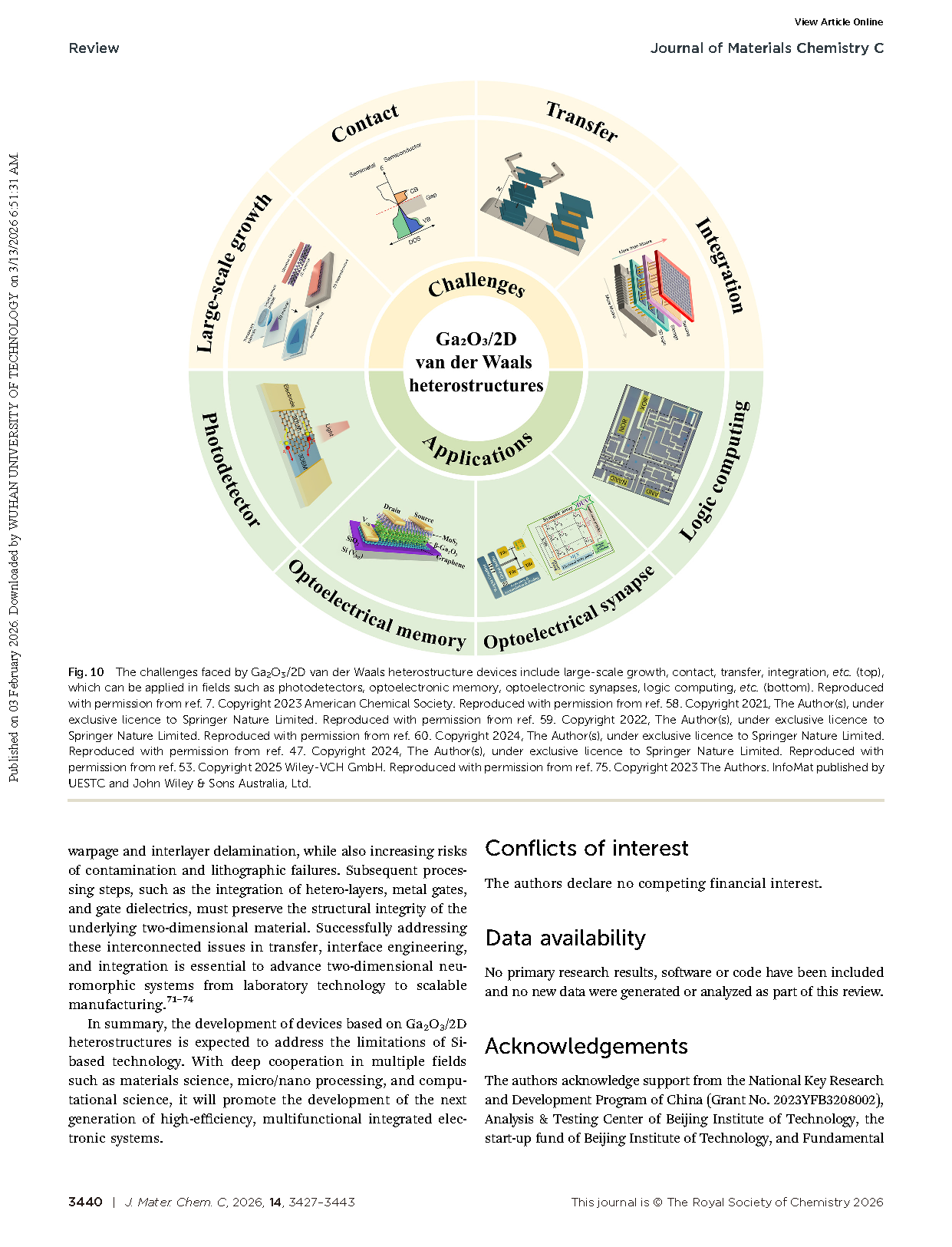
Fig. 10 The challenges faced by Ga2O3/2D van der Waals heterostructure devices include large-scale growth, contact, transfer, integration, etc. (top), which can be applied in fields such as photodetectors, optoelectronic memory, optoelectronic synapses, logic computing, etc. (bottom).
DOI:
doi.org/10.1039/D5TC04478B