Paper Sharing
【Member Papers】Trap-mediated current transport in tunneling layer of Ni/Al₂O₃/β-Ga₂O₃ diodes: effect of proton irradiation
日期:2026-04-13阅读:225
Associate Professor Leidang Zhou's Team from Xi'an Jiaotong University has published a paper titled “Trap-mediated current transport in tunneling layer of Ni/ Al2O3/β-Ga2O3 diodes: effect of proton irradiation” in the academic journal Applied Surface Science.
Background
High-energy protons prevalent in space environments can easily cause severe displacement damage and single-particle effects, posing a significant challenge to the reliability of β-Ga2O3 devices. Therefore, the pursuit of high-performance β-Ga2O3 devices with potential radiation tolerance and elucidating the underlying mechanisms of proton irradiation effects on the device performance are critical issues requiring in-depth investigation for the current application and radiation-hardening design of β-Ga2O3 devices. The electrical characteristics and radiation resistance of β-Ga2O3 devices are influenced by heterojunction terminal design. In contrast to Schottky barrier diodes (SBDs), β-Ga2O3 metal-insulator-semiconductor diodes (MISDs) with a nanometer-thick insulator layer for interface modification demonstrate significant improvements in leakage current suppression and breakdown voltage, as exemplified by MISDs based on AlN, Al reaction interface layers, Nb2O5, and TiO2. Notably, GaN-based MIS-high electron mobility transistors (MIS-HEMTs) demonstrate superior proton radiation resistance over conventional HEMTs, which implies the intrinsic radiation-hardening potential of the MIS structure, i.e., a thin Al2O3 layer. Nevertheless, systematic investigation into the effects of proton irradiation on β-Ga2O3 MISDs remains scarce.
Abstract
The radiation tolerance of ultrawide-bandgap gallium oxide (β-Ga2O3) devices has been a critical research frontier for their application in extreme irradiation environments. While metal-insulator-semiconductor diodes (MISDs) exhibit superior reliability compared to Schottky barrier diodes (SBDs), their radiation tolerance has not been comprehensively unveiled. Herein, high-performance Ni/Al2O3/β-Ga2O3 MISDs are fabricated by incorporating 3-nm Al2O3 layer and employing supercritical fluid treatment. The subsequent 5 MeV proton irradiation of MISDs reveals concurrent degradation in both forward and reverse characteristics, distinct from that observed in SBDs. The divergence primarily stems from proton-induced generation of oxygen vacancy electron traps within Al2O3. On one hand, the comparative analysis between proton and γ-ray irradiation damage unravels the competitive interplay between electron traps within Al2O3 and series resistance in governing the on-state current. On the other hand, the transition of the leakage current after proton irradiation from a positive to a negative temperature dependence at high bias confirms a shift in the dominant leakage mechanism, which is no longer consistent with Poole-Frenkel emission and Fowler-Nordheim tunneling. This research provides detailed insights into the irradiation damage mechanism of β-Ga2O3 devices with MIS structure, guiding the establishment of design strategies for highly reliable β-Ga2O3 devices suitable for future space applications.
Highlights
High-performance Ni/Al2O3/β-Ga2O3 MISDs were fabricated by incorporating 3-nm Al2O3 layer and employing supercritical fluid treatment.
The distinct performance degradation under proton irradiation between MISDs and Ni/β-Ga2O3 SBDs originates from radiation-induced traps within Al2O3.
The current transport mechanism in as-fabricated and irradiated MISDs is elucidated.
A physical model is established to differentiate between the on-state current responses to proton and γ-ray irradiation.
Conclusion
The study systematically investigates the proton irradiation damage mechanism in high-performance Ni/Al2O3/β-Ga2O3 MISDs fabricated by incorporating 3-nm Al2O3 layer and employing SCF treatment. The main conclusions are as follows:
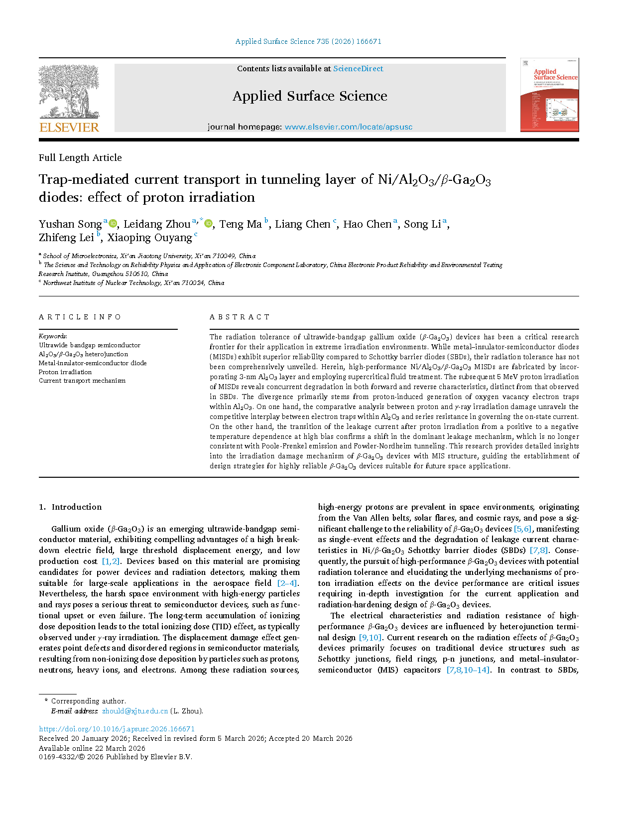
(i) After proton irradiation, MISDs exhibited a 44% smaller increase in Ron,sp than SBDs. Nevertheless, despite their initial leakage superiority, MISDs suffered from a substantial leakage current increase with intensified inhomogeneity, in sharp contrast to the reduced leakage current observed in SBDs.
(ii) Both ionization and displacement damage induced by proton irradiation in Al2O3 contribute to the increase of Nt and Neff, whereas the carrier removal effect induced by displacement damage dominates in β-Ga2O3. Furthermore, irradiation-induced defects modify the band alignment of Al2O3/β-Ga2O3 heterojunction, as manifested by an increase of ΔEC and a transition of ΔEV from positive to negative.
(iii) The forward current primarily follows TFE model in the subthreshold region and TAT model under on-state conditions. The on-state current is determined by the competitive interplay between the electron traps in Al2O3 and Rs in β-Ga2O3, contributing to the opposite trends in on-state current after proton and γ-ray irradiation.
(iv) The leakage current of as-fabricated MISDs adheres to the typical transition in mechanisms from PFE at low bias to FNT at higher bias. In contrast, the leakage current of proton-irradiated MISDs exhibits a positive temperature dependence at low bias and a negative dependence at higher bias, confirming the dominance of the TAT process.
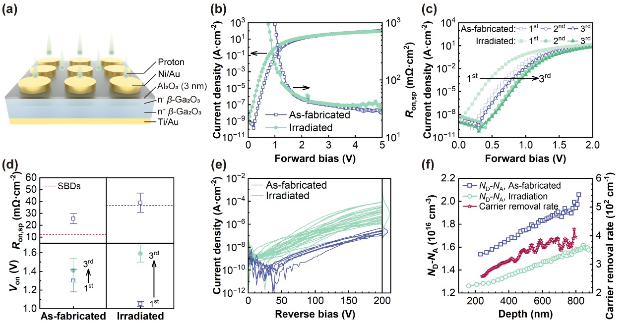
Fig. 1. Room-temperature electrical characteristics of as-fabricated and proton-irradiated Ni/Al2O3/β-Ga2O3 metal-insulator-semiconductor diodes (MISDs). (a) Schematic diagram of the MISDs exposed to proton irradiation. (b) Forward current density-voltage (J-V) characteristics and specific on-resistance (Ron,sp). (c) Forward J-V characteristics with multiple unidirectional sweeps. (d) Statistical distribution of Ron,sp and turn-on voltage (Von) at 1 A·cm−2. (e) Reverse J-V characteristics and statistical distribution of leakage current density at −200 V. (f) Net carrier concentration (ND−NA) and carrier removal rate.
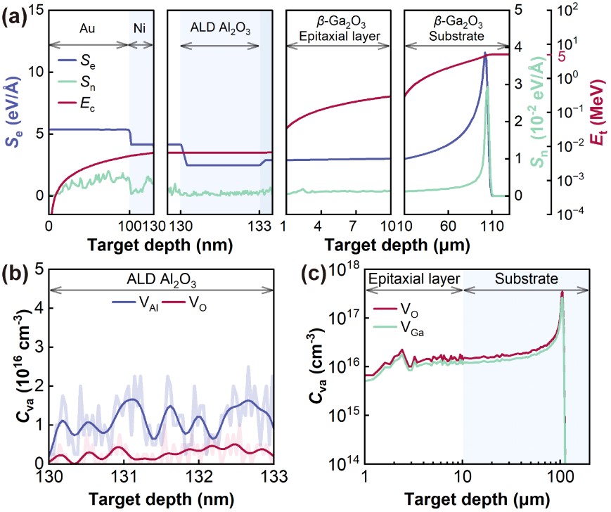
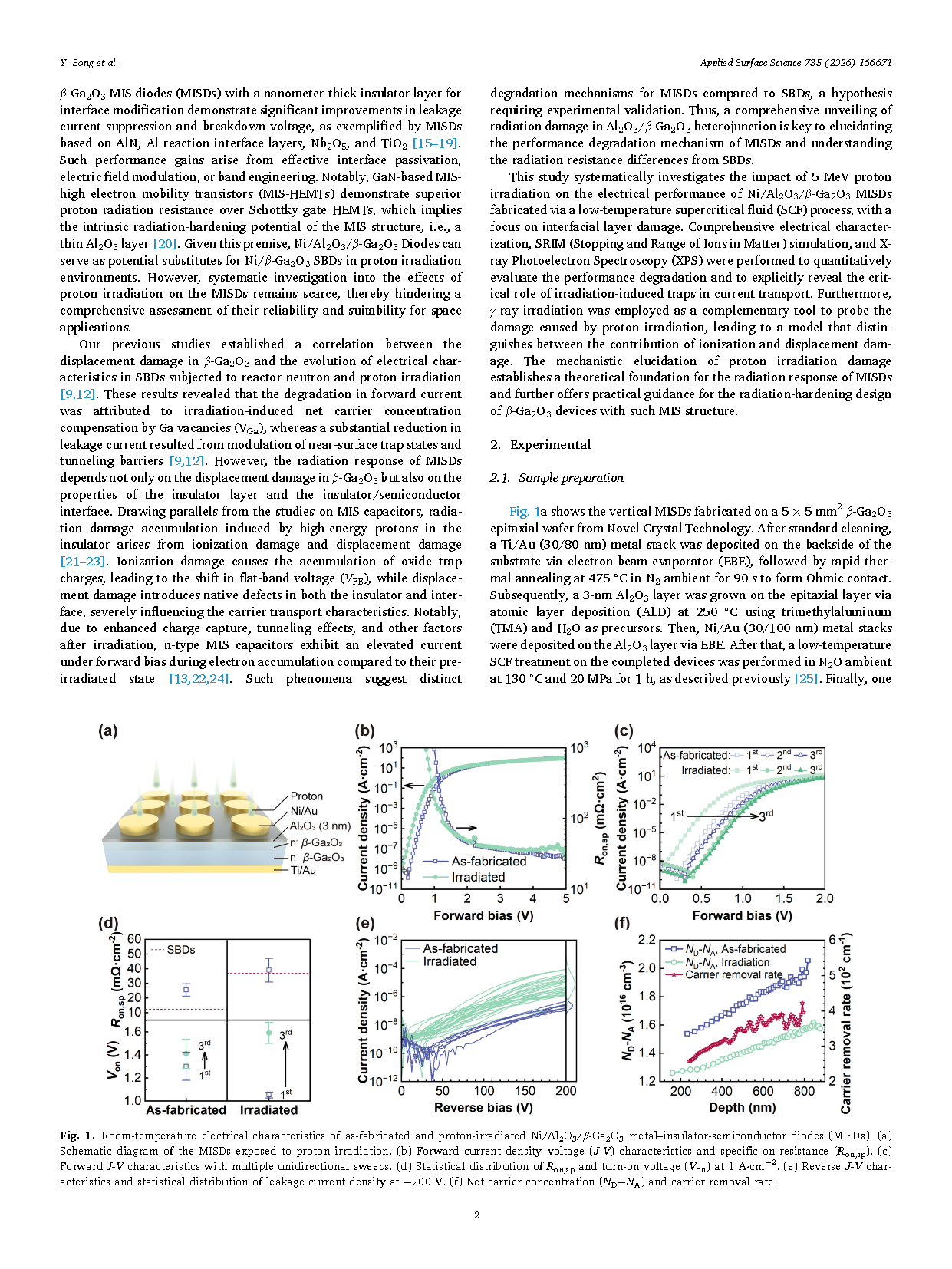
Fig. 2. The SRIM simulation results. (a) Electronic energy loss (Se), nuclear energy loss (Sn), and cumulative energy loss (Ec) as a function of depth. Depth profiles of vacancies in (b) Al2O3 and (c) β-Ga2O3.
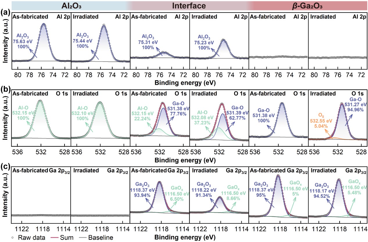
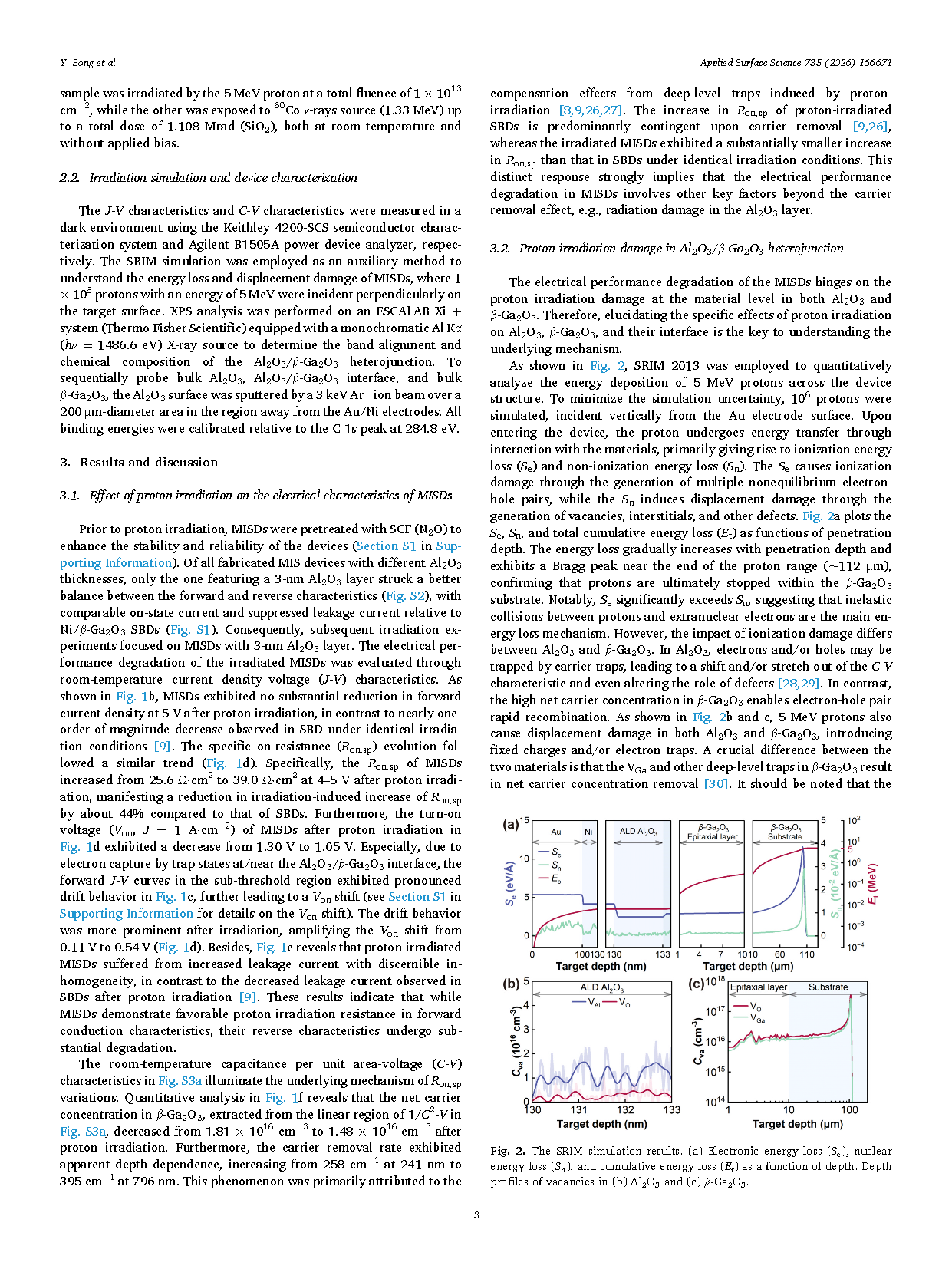
Fig. 3. XPS spectra of as-fabricated and proton-irradiated Al2O3/β-Ga2O3 heterojunctions. Core-level spectra of (a) Al 2p, (b) O 1s, and (c) Ga 2p3/2 collected from the bulk Al2O3, Al2O3/β-Ga2O3 interface, and bulk β-Ga2O3.
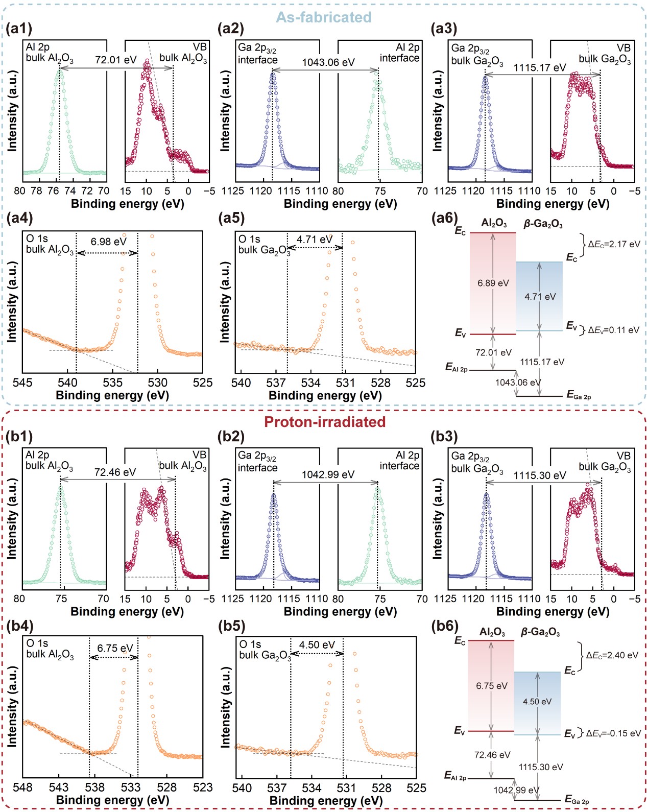
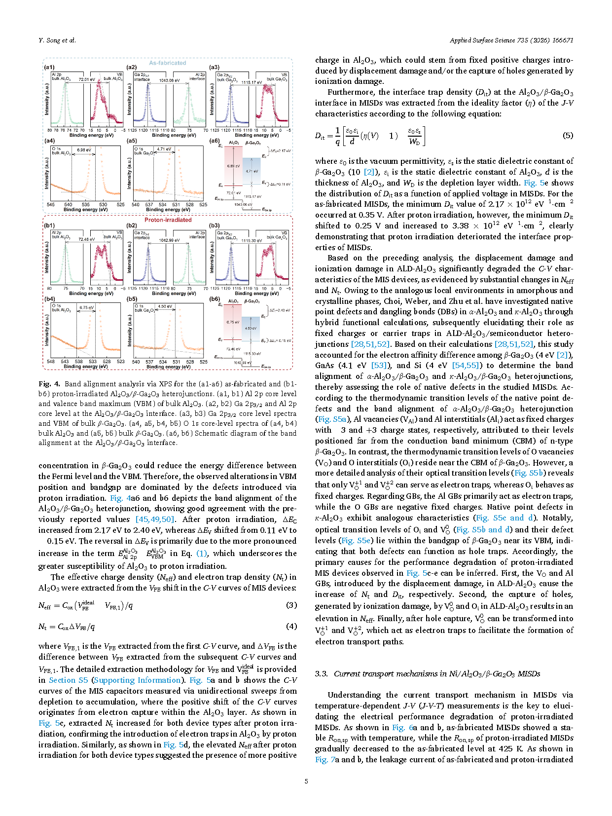
Fig. 4. Band alignment analysis via XPS for the (a1-a6) as-fabricated and (b1-b6) proton-irradiated Al2O3/β-Ga2O3 heterojunctions. (a1, b1) Al 2p core level and valence band maximum (VBM) of bulk Al2O3. (a2, b2) Ga 2p3/2 and Al 2p core level at the Al2O3/β-Ga2O3 interface. (a3, b3) Ga 2p3/2 core level spectra and VBM of bulk β-Ga2O3. (a4, a5, b4, b5) O 1s core-level spectra of (a4, b4) bulk Al2O3 and (a5, b5) bulk β-Ga2O3. (a6, b6) Schematic diagram of the band alignment at the Al2O3/β-Ga2O3 interface.
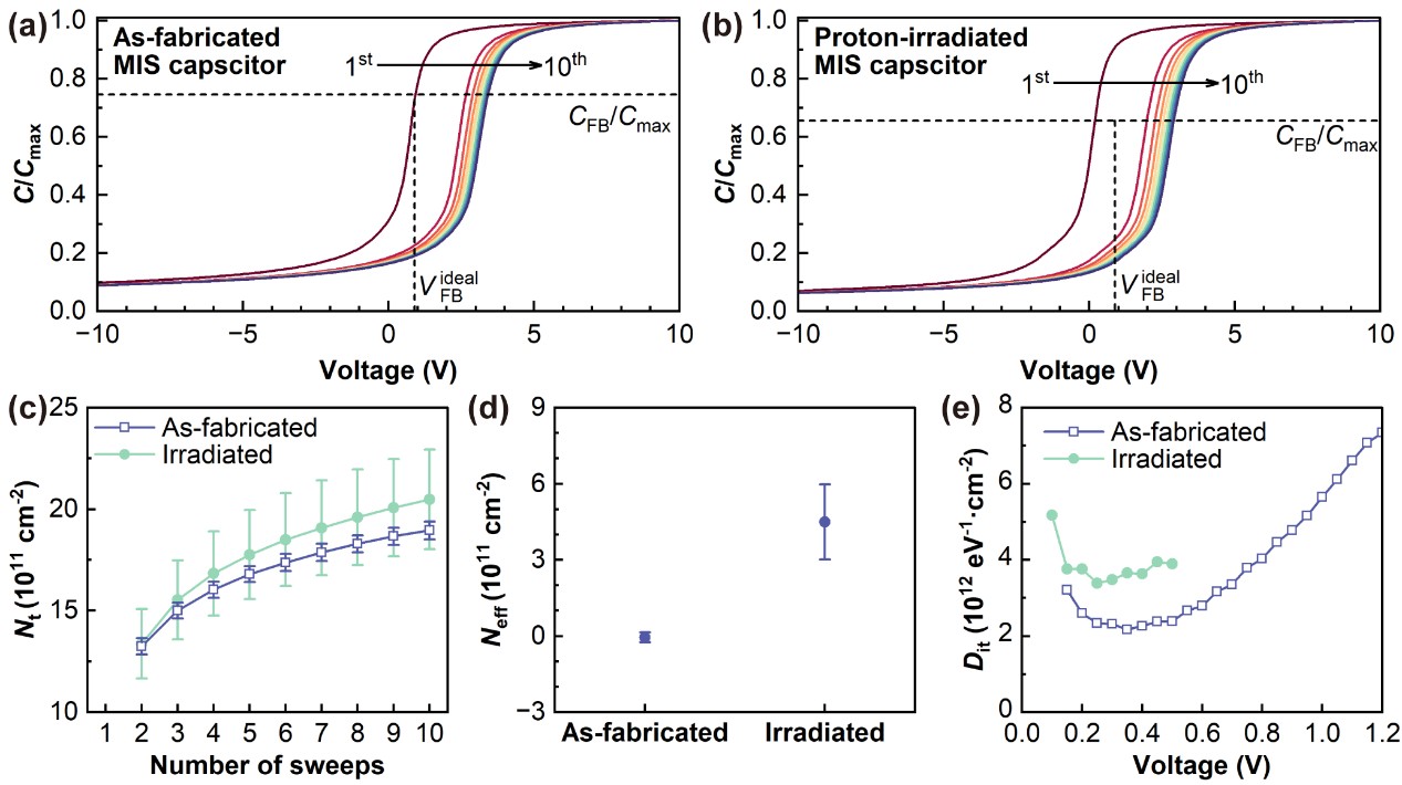
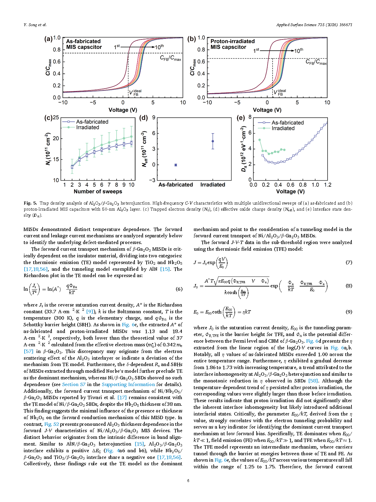
Fig. 5. Trap density analysis of Al2O3/β-Ga2O3 heterojunction. High-frequency C-V characteristics with multiple unidirectional sweeps of (a) as-fabricated and (b) proton-irradiated MIS capacitors with 50-nm Al2O3 layer. (c) Trapped electron density (Nt), (d) effective oxide charge density (Neff), and (e) interface state density (Dit).
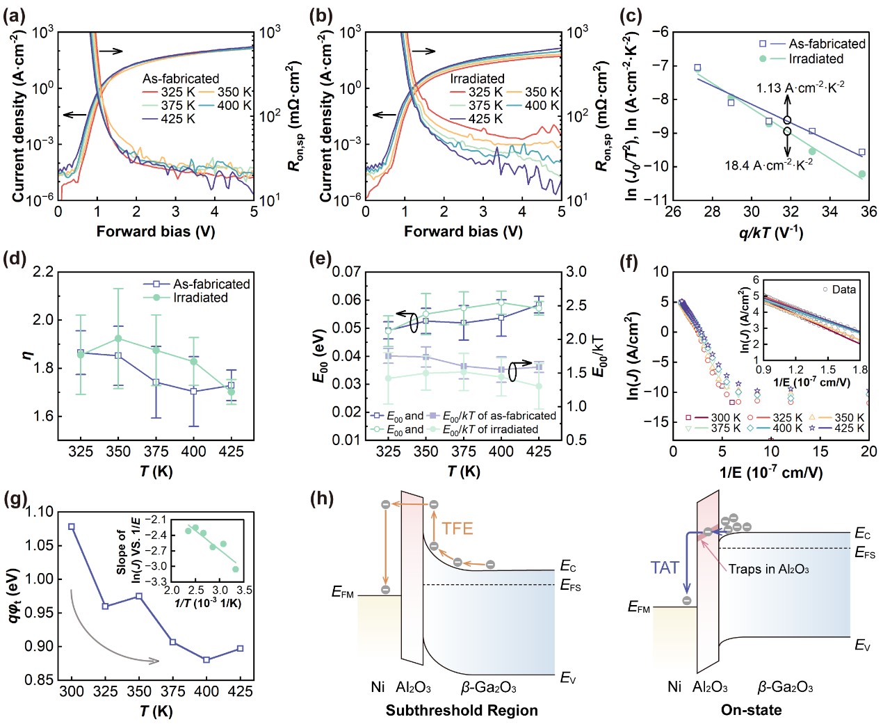
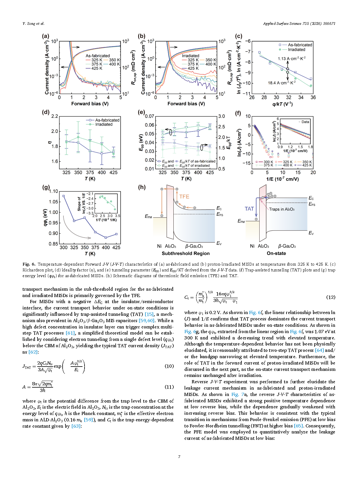
Fig. 6. Temperature-dependent Forward J-V (J-V-T) characteristics of (a) as-fabricated and (b) proton-irradiated MISDs at temperatures from 325 K to 425 K. (c) Richardson plot, (d) ideality factor (η), and (e) tunneling parameter (E00) and E00/KT derived from the J-V-T data. (f) Trap-assisted tunneling (TAT) plots and (g) trap level (qφt) for as-fabricated MISDs. (h) Schematic diagrams of thermionic field emission (TFE) and TAT.
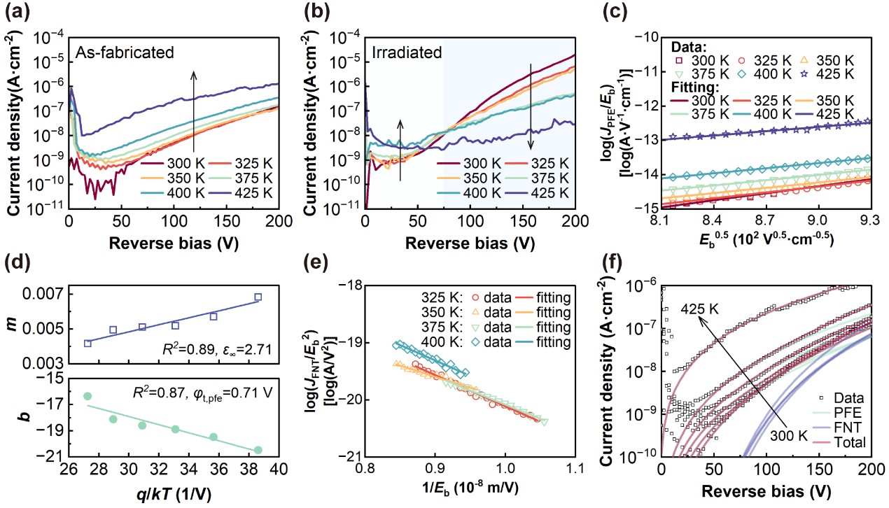
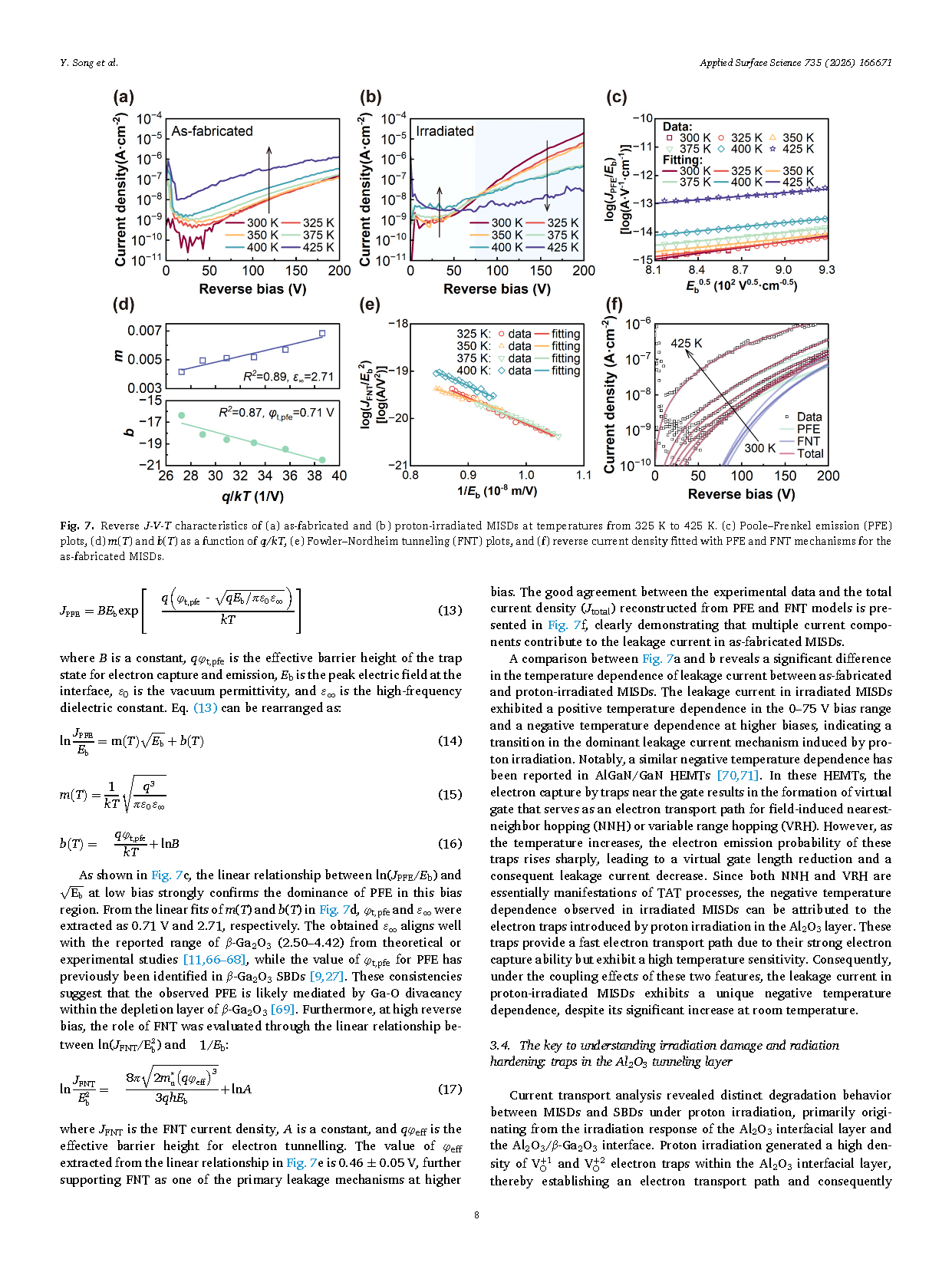
Fig. 7. Reverse J-V-T characteristics of (a) as-fabricated and (b) proton-irradiated MISDs at temperatures from 325 K to 425 K. (c) Poole–Frenkel emission (PFE) plots, (d) m(T) and b(T) as a function of q/kT, (e) Fowler–Nordheim tunneling (FNT) plots, and (f) reverse current density fitted with PFE and FNT mechanisms for the as-fabricated MISDs.
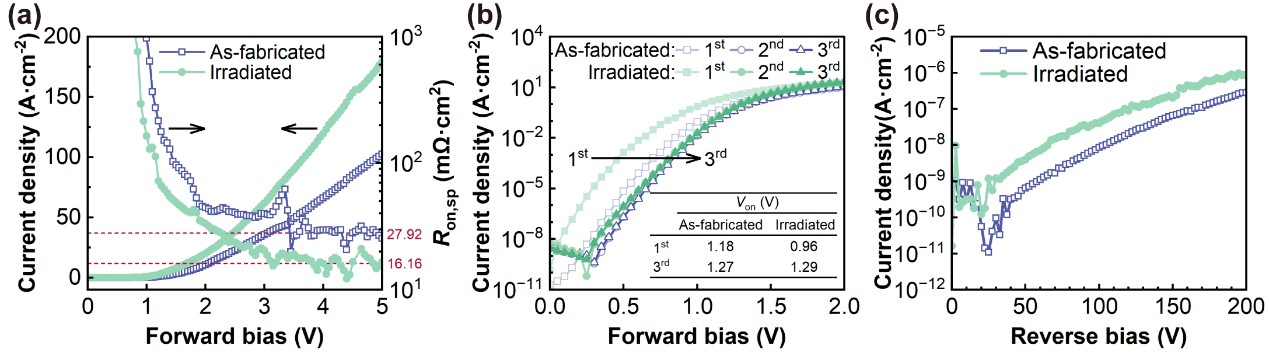
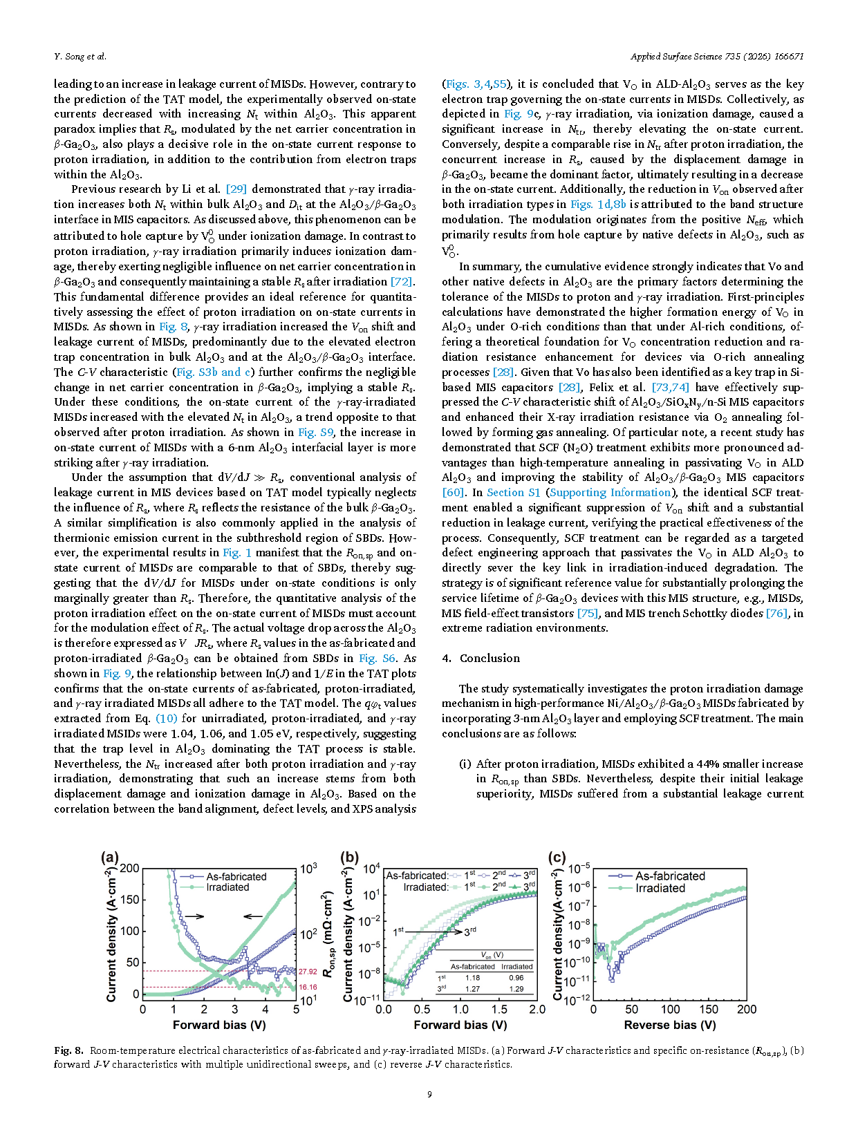
Fig. 8. Room-temperature electrical characteristics of as-fabricated and γ-ray-irradiated MISDs. (a) Forward J-V characteristics and Ron,sp, (b) forward J-V characteristics with multiple unidirectional sweeps, and (c) reverse J-V characteristics.
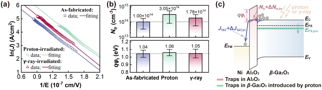
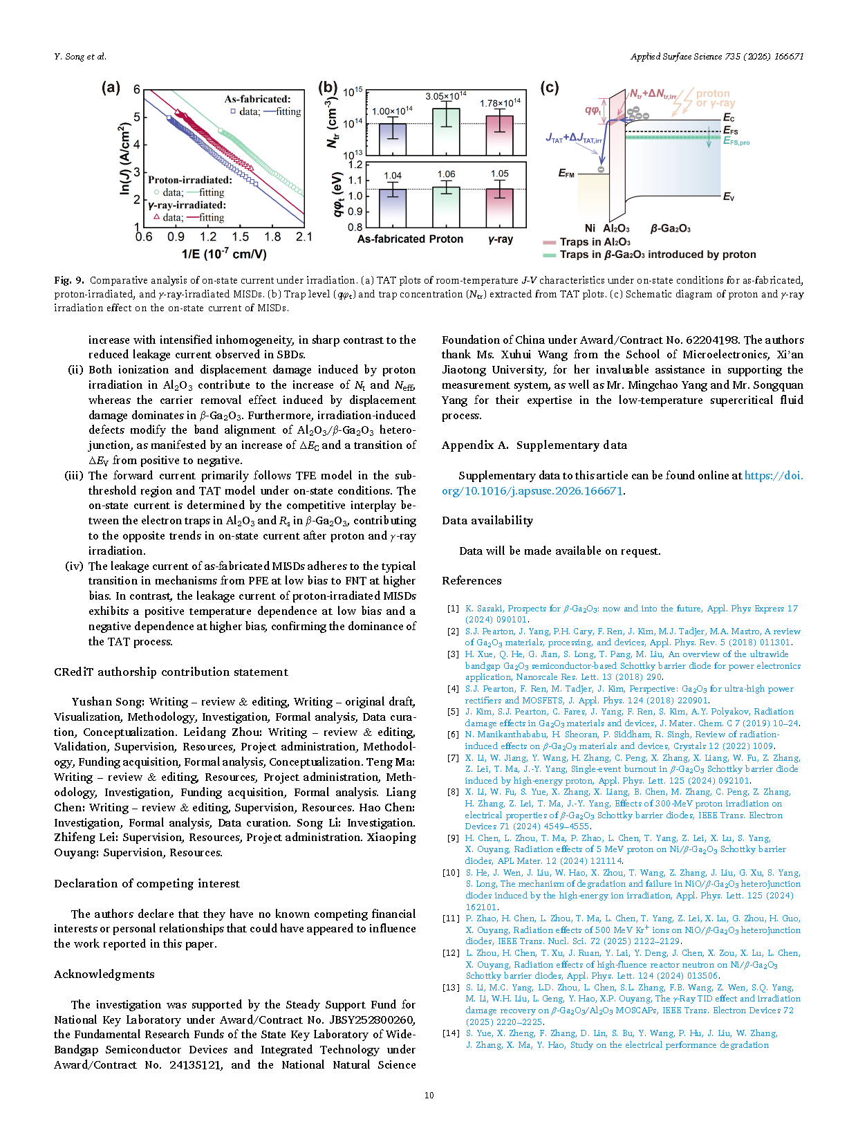
Fig. 9. Comparative analysis of on-state current under irradiation. (a) TAT plots of room-temperature J-V characteristics under on-state conditions for as-fabricated, proton-irradiated, and γ-ray-irradiated MISDs. (b) qφt and trap concentration (Ntr) extracted from TAT plots. (c) Schematic diagram of proton and γ-ray irradiation effect on the on-state current of MISDs.
DOI:
doi.org/10.1016/j.apsusc.2026.166671