Paper Sharing
【Member Papers】High-performance solar-blind UV photodetector based on Ti₃C₂Tₓ MXene/α-Ga₂O₃ heterojunction
日期:2026-04-13阅读:256
Researchers from Nanjing University of Posts and Telecommunications, Hong Kong University of Science and Technology (Guangzhou), Xi’an Jiaotong-Liverpool University and Hong Kong University of Science and Technology have published a dissertation titled “High-performance solar-blind UV photodetector based on Ti₃C₂Tₓ MXene/α‑Ga₂O₃ heterojunction” in Applied Physics Letters.
Background
Solar-blind UV detection is crucial in military security, environmental monitoring and other fields. α‑Ga₂O₃ has become an ideal candidate due to its ultrawide bandgap. Constructing heterojunction between 2D MXene and α‑Ga₂O₃ can improve carrier separation efficiency through interface built-in electric field. However, the research on Ti₃C₂Tₓ / metastable α‑Ga₂O₃ heterojunction is very limited at present, which can hardly meet the development requirements of high-performance and low-power devices.
Abstract
The integration of two-dimensional MXenes with ultrawide bandgap semiconductors presents a novel pathway for high-performance optoelectronics. However, the coupling of Ti₃C₂Tₓ with the corundum metastable α‑phase of gallium oxide (α‑Ga₂O₃) with wider bandgap than conventional β‑phase remains largely unexplored. In this work, we demonstrate a high-sensitivity solar-blind ultraviolet photodetector based on a Ti₃C₂Tₓ MXene/α‑Ga₂O₃ heterojunction, fabricated via mist chemical vapor deposition (mist-CVD) and spray-coating techniques. The resulting device exhibits superior optoelectronic performance, achieving a remarkably high photoresponsivity of 31.1 mA/W and an ultralow dark current of 0.41 pA under 254 nm illumination. This enhanced performance is attributed to the formation of high-quality Schottky junction at the MXene and α‑Ga₂O₃ interface, where a work function difference creates a built-in electric field that facilitates efficient carrier separations. Notably, the responsivity of this architecture surpasses that of state-of-the-art α‑Ga₂O₃‑based photodetectors, establishing the Ti₃C₂Tₓ/α‑Ga₂O₃ heterostructure as a promising candidate for next-generation, low-power deep-UV sensing applications.
Highlights
First realization of heterojunction construction between Ti₃C₂Tₓ MXene and metastable α‑Ga₂O₃ for high-performance solar-blind UV photodetectors.
Fabrication of devices via vacuum-free and scalable mist-CVD and spray-coating techniques with simple and mass-producible process.
Formation of strong built-in electric field at heterojunction interface, significantly improving carrier separation efficiency and achieving high responsivity of 31.1 mA/W.
Device achieves ultralow dark current of 0.41 pA and ultrahigh specific detectivity of 1.92×10¹³ Jones, with comprehensive performance superior to similar Ga₂O₃‑based detectors.
The device maintains stable photoelectric response after 30 days of exposure to ambient air at room temperature, exhibiting excellent environmental stability.
Conclusion
In summary, we have successfully demonstrated a high-performance solar-blind UV photodetector by integrating spray-coated Ti₃C₂Tₓ MXene with mist-CVD grown α‑Ga₂O₃. The device exhibits robust photoresponse behavior and superior optoelectronic performance, characterized by a low dark current of 0.41 pA @ −5 V bias and a remarkably high photoresponsivity of 31.1 mA/W. This substantial work function difference between the materials induces a Schottky junction with a strong built-in electric field, enabling efficient photogenerated carrier separation. Notably, this device surpasses the responsivity of other α‑Ga₂O₃‑based photodetectors under similar low-voltage conditions. These findings establish the MXene/α‑Ga₂O₃ interface as a highly competitive candidate for next-generation deep-UV sensing, offering a promising pathway for the development of low-power, high-sensitivity optoelectronic systems.
Project Support
This work was supported by the C. K. Tan start-up fund from the Hong Kong University of Science and Technology (Guangzhou); Guangzhou Municipal Science and Technology Project Nos. 2023A03J0003, 2023A03J0013, 2023A04J0310, and 2023A03J0152; the Department of Education of Guangdong Province (No. 2024ZDZX1005); the State Administration of Foreign Experts Affairs (No. Y20240005); the Matching Funding for Selected Talent of National Programs (No. CZ118SC24007); the National Major Talent Project (No. CZ118SC25005); and the Excellent Young Scientists Fund (overseas): RK118QN24006 and RK118QN25006. This work was also supported by the Materials Characterization and Preparation Facility (MCPF) and Green Materials Laboratory at the Hong Kong University of Science and Technology (Guangzhou).
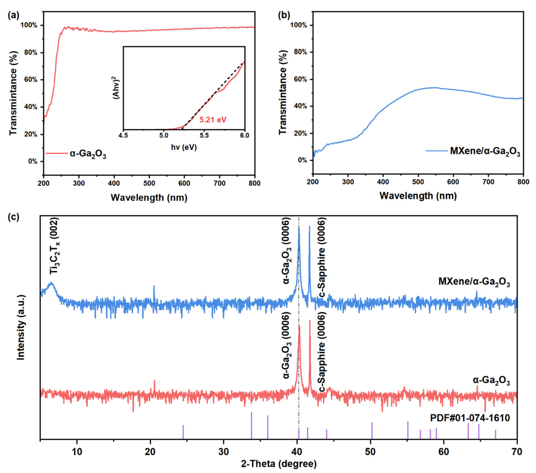
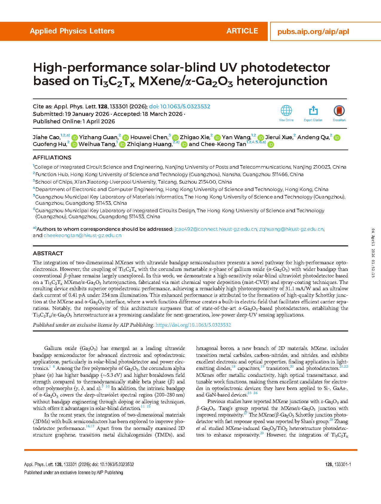
Fig. 1. Transmittance (T%) of α‑Ga₂O₃ (a) and MXene/α‑Ga₂O₃ (b) measured using a UV-Vis system, XRD patterns of gallium oxide thin film on c-plane sapphire with JCPDS reference (c).
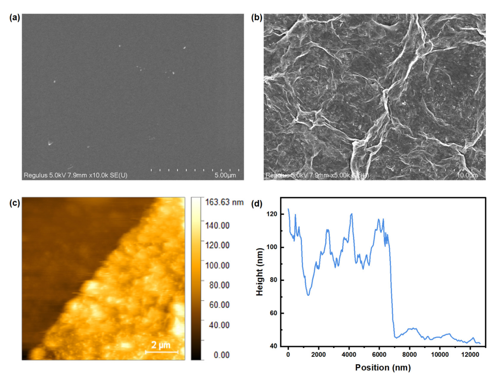
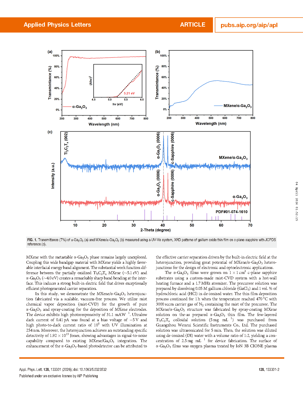
Fig. 2. SEM image of α‑Ga₂O₃ film surface (a), deposited MXene (b), AFM image of the MXene/α‑Ga₂O₃ surface and interface (c), and the height profile image (d).
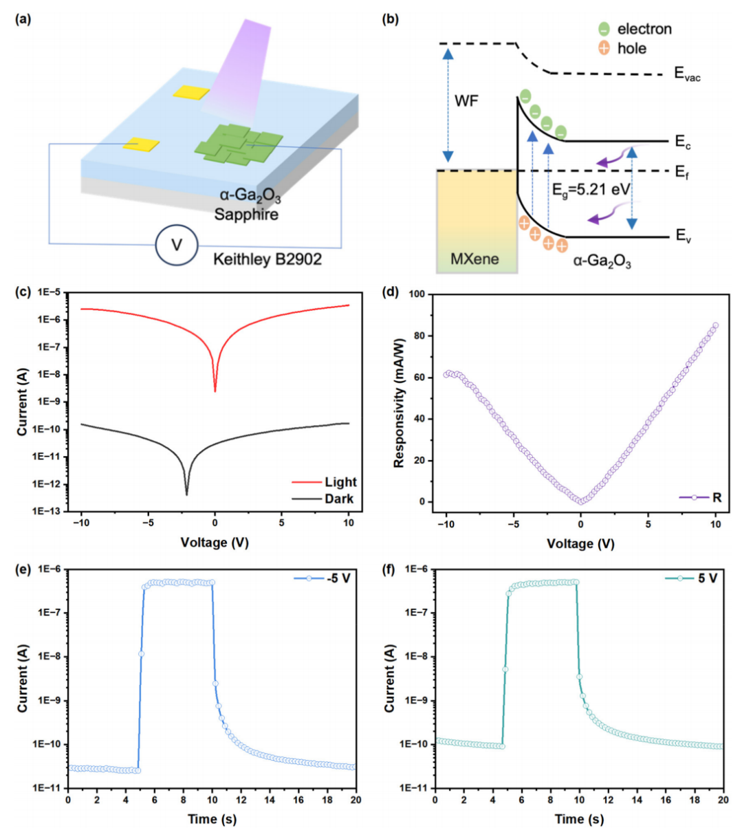
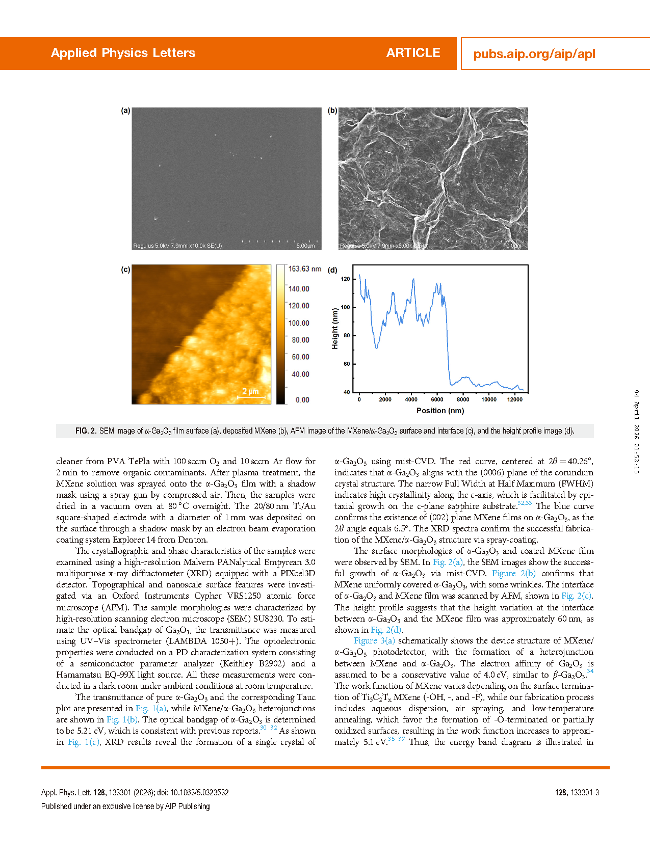
Fig. 3. Schematic diagram of MXene/α‑Ga₂O₃ photodetector (a), energy band diagram of MXene/α‑Ga₂O₃ heterojunction (b). Photoelectric properties of MXene/α‑Ga₂O₃ heterojunction. Typical I–V characteristics of MXene/α‑Ga₂O₃ heterojunction under dark and 254 nm UV light illumination (c), photoresponsivity (d), response time of photodetector at 5 V (e) and at −5 V (f).
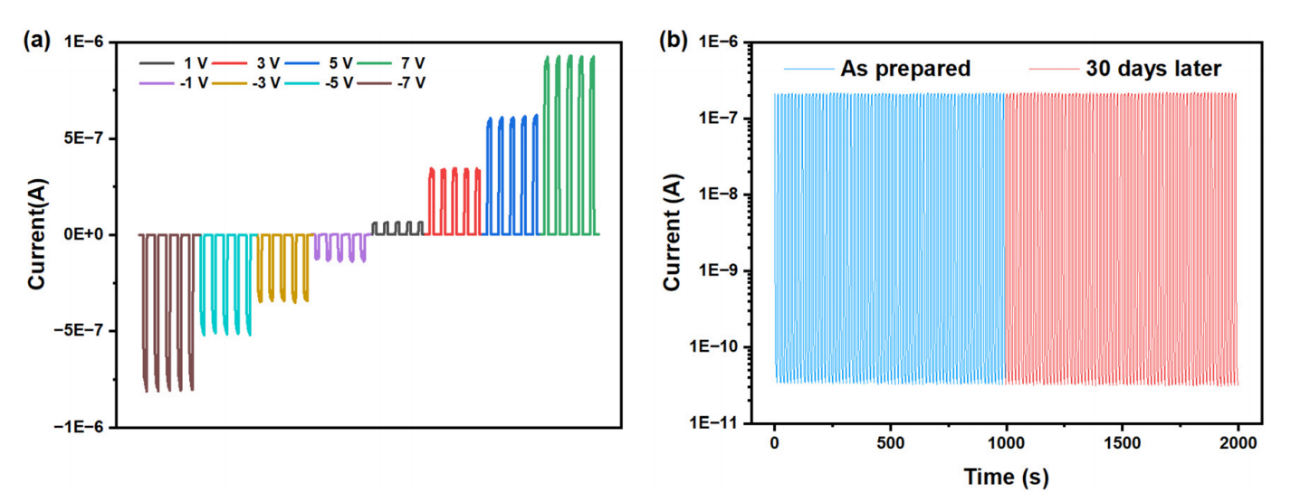
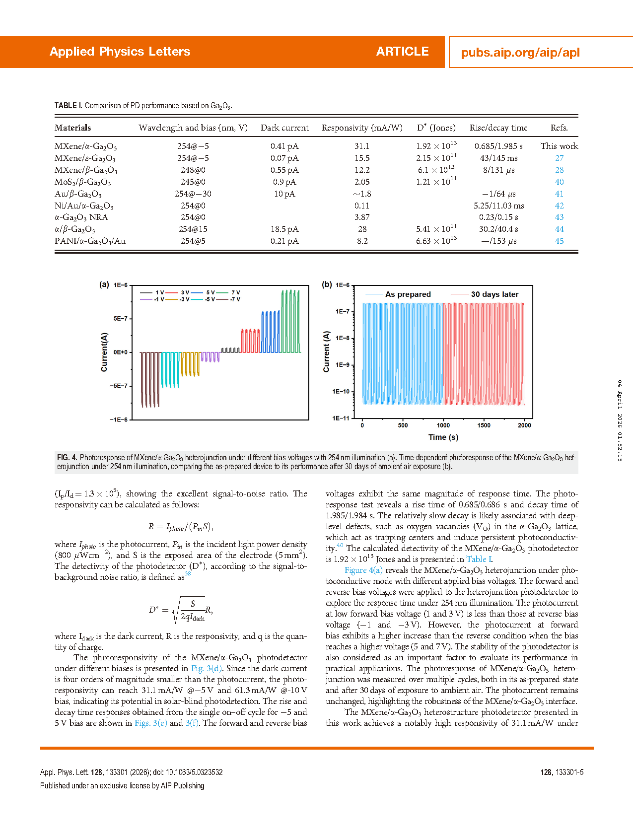
Fig. 4. Photoresponse of MXene/α‑Ga₂O₃ heterojunction under different bias voltages with 254 nm illumination (a). Time-dependent photoresponse of the MXene/α‑Ga₂O₃ heterojunction under 254 nm illumination, comparing the as-prepared device to its performance after 30 days of ambient air exposure (b).
DOI:
doi.org/10.1063/5.0323532