Paper Sharing
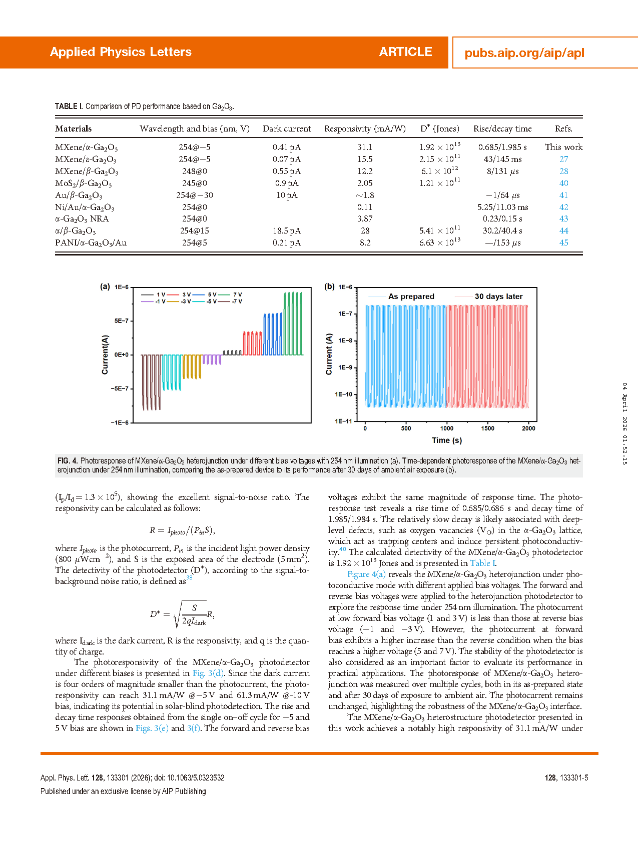
【Member Papers】High-performance solar-blind UV photodetector based on Ti₃C₂Tₓ MXene/α-Ga₂O₃ heterojunction
日期:2026-04-14阅读:199
Researchers from Hunan University of Science and Engineering, Xiamen University, and Hunan University have published a dissertation titled “Tuning the structural, electronic, and transport properties of ferroelectric‑zinc blende phase Ga₂O₃ monolayer by Si dopant and biaxial strain” in Materials Science & Engineering: B.
Background
Two‑dimensional (2D) Ga₂O₃ has a wide range of applications in flexible optoelectronic devices. Recently, a novel 2D Ga₂O₃ monolayer with ferroelectric‑zinc blende (FZB) phase has been theoretically predicted, but systematic studies on its electronic structure and carrier mobility are still insufficient. Different from the strong anisotropy of conventional β‑Ga₂O₃, FZB‑Ga₂O₃ exhibits high structural symmetry and isotropic characteristics. Silicon (Si) doping is an effective method to regulate the electronic structure of Ga₂O₃, and strain engineering can further realize the continuous modulation of band structure and transport properties. Based on first‑principles calculations, the team systematically studied the structural stability, strain‑tunable band structure, and carrier transport properties of Si‑doped FZB‑Ga₂O₃ monolayers, aiming to provide theoretical support for the design and application of novel 2D wide‑bandgap semiconductors.
Abstract
Two‑dimensional (2D) materials have emerged with extensive applications in flexible optoelectronic devices. Recently, the 2D Ga₂O₃ crystal structure with ferroelectric‑zinc blende (FZB‑Ga₂O₃) phase structure was predicted, while further studies of the electronic properties and carrier mobilities are absent. In this work, the structural stabilities, strain‑modified band structures and carrier transports of Si‑doped FZB‑Ga₂O₃ monolayer are investigated using Perdew–Burke–Ernzerhof (PBE) and Heyd–Scuseria–Ernzerhof (HSE) hybrid functionals alongside deformation potential theory. Si‑doped FZB‑Ga₂O₃ monolayer exhibits the effective n‑type doping behavior, where the bandgaps increase from 1.43 to 1.60 eV by PBE and 3.58 to 3.63 eV by HSE. Applying −6% compressive to 6% tensile biaxial strains, the bandgaps decrease dramatically of ~1.4 eV, which are corroborated by the rapid upward shifts of the VBM dominated by π bonding of O‑2p, Si‑3p, and Ga‑3d orbitals compared to the CBM consisted by σ* anti‑bonding states derived from hybridized Ga‑4s, Ga‑4p, Si‑3s, and O‑2p orbitals. With strain modulations, the μₑₓ alters from 655.21 to 929.43 cm² V⁻¹ s⁻¹, while the μₑᵧ changes from 703.48 to 1037.29 cm² V⁻¹ s⁻¹. The highest μₑₓ and μₑᵧ occurring at 4% tensile strain within +6 strain modulations can be ascribed to the weaker quantum confinement effect. Moreover, the anisotropy is within the range between 1.07 and 1.21, indicating a strong isotropy of electron mobility in Si‑doped FZB‑Ga₂O₃ monolayer due to its high structure symmetries, instead of the pronounced anisotropy in β‑Ga₂O₃. Therefore, the exceptional stability, strain‑tunable electronic property and robust isotropy of electron mobility in Si‑doped FZB‑Ga₂O₃ monolayer underscore its strong potential for nanoscale optoelectronic devices.
Highlights
Systematically investigate the structural, electronic, and transport properties of Si‑doped ferroelectric‑zinc blende FZB‑Ga₂O₃ monolayer for the first time
Verify that Si atoms preferentially occupy the six‑coordinated GaII sites with excellent dynamic and thermodynamic stability
Reveal the continuous modulation mechanism of biaxial strain on bandgap with a tunable range up to ~1.4 eV
Achieve highly isotropic and high electron mobility up to 1037.29 cm² V⁻¹ s⁻¹
Clarify the regulation law of quantum confinement effect and structural symmetry on carrier transport
Conclusion
The structural stabilities, strain‑modified band structures, and carrier transport properties of Si‑doped FZB‑Ga₂O₃ monolayer are investigated using PBE and HSE functionals alongside DP theory. Si dopant preferentially occupies the six‑coordinated GaII site with excellent dynamic and thermodynamical stabilities, instead of four‑coordinated GaI as reported in Si‑doped cleaved 2D β‑Ga₂O₃, which can be ascribed to the various local structures and atomic Ga positions. Charge density difference reveals significant charge redistributions where Si impurity losses 3.09e charge into the SiGaⅡ monolayer structure. The band structure after Si doping indicates an effective n‑type doping behavior with a slightly increased bandgap value of ~3.6 eV, renders it promising for flexible UV photodetectors. Applying ±6% biaxial strain modulations, the bandgaps decrease from 4.05 eV to 2.65 eV, which is primarily result from the more rapid upward shift of the VBM compared to the CBM that are related to the bonding states variations. In the Si‑doped FZB‑Ga₂O₃ monolayer, the CBM consists of σ* anti‑bonding states derived from hybridized Ga‑4s, Ga‑4p, Si‑3s, and O‑2p orbitals, while the VBM is dominated by π bonding formed by O‑2p, Si‑3p, and Ga‑3d orbitals. Increasing tensile or compressive strains, the σ* anti‑bonding and π bonding states can be pushed up and down, leading to the energy raises and lowers of both CBM and VBM, respectively. As the compressive strains various from −6% to 6%, the μₑₓ alters from 655.21 to 929.43 cm² V⁻¹ s⁻¹, while the μₑᵧ changes from 703.48 to 1037.29 cm² V⁻¹ s⁻¹. The highest μₑₓ and μₑᵧ for the SiGaⅡ monolayer occur at 4% tensile strain, which can be ascribed to the weaker quantum confinement effect as determined by the spatial charge distributions at the CBM. Moreover, the electron mobility anisotropy is within the range between 1.07 and 1.21, indicating a strong isotropy of the 2D SiGaⅡ monolayer, which is distinct from the strong anisotropy in 2D β‑Ga₂O₃. Besides, the team predict that the SiC substrate is endowed with highest electron mobility among common hexagonal substrates including SiC, Si (111), sapphire, GaN, AlN, and ZnO. Overall, the exceptional stabilities, strain‑tunable electronic properties and robust isotropy of electron mobility in Si‑doped FZB‑Ga₂O₃ monolayer underscore its strong potential for flexible electronic and other nanoscale optoelectronic devices. However, one of the possible challenges is achieving effective p-type FZB-Ga₂O₃ in terms of the flat VBM.
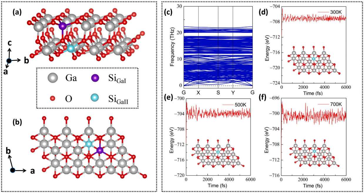
Fig. 1. The Si‑doped FZB‑Ga₂O₃ monolayer structure from (a) perspective view and (b) top view. Panel (c): phonon dispersion spectrum of SiGaⅡ monolayer structure. AIMD simulations of SiGaⅡ monolayer structure at (d) 300 K, (e) 500 K, and (f) 700 K. The inserts in Fig. 1(d–f) indicate its relaxed structures.
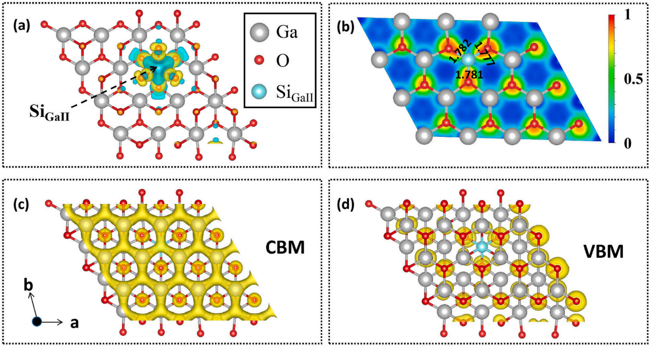
Fig. 2. (a) Charge density difference of SiGaⅡ monolayer. The isosurface value is set as 0.005 e/ ų. The loss and gain of charges are denoted by the cyan and yellow colors, respectively. (b) ELF of the SiGaⅡ monolayer. (c) Partial charge density of VBM and (d) CBM of SiGaⅡ monolayer with the isosurface value of 0.001 e/ ų.
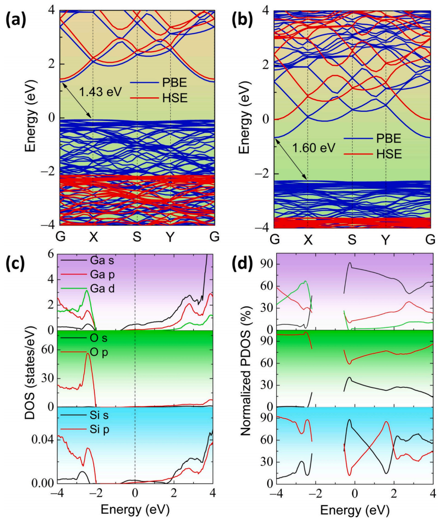
Fig. 3. The calculated band structures of (a) FZB‑Ga₂O₃ monolayer and (b) SiGaⅡ under PBE and HSE methods. The (c) PDOS and (d) normalized PDOS of Ga, O, and Si orbitals for SiGaⅡ monolayer using PBE functional.
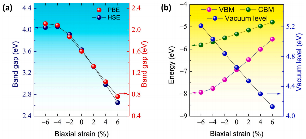
Fig. 4. (a) The biaxial strain dependences of the bandgaps in the SiGaⅡ monolayer. (b) The strain evolutions of the vacuum level energies and the corresponding shifts of the VBM and CBM relative to this vacuum reference.
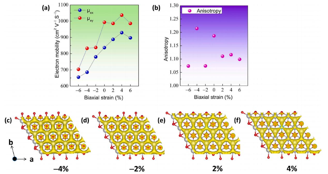
Fig. 5. (a) Electron mobility and (b) anisotropy of SiGaⅡ monolayer under various biaxial strains. Partial charge distributions at the CBM with various strain cases: (c) −4%, (d) −2%, (e) 2%, and (f) 4%. The isosurface level is 0.001 e/ ų.
DOI:
doi.org/10.1016/j.mseb.2026.119405