Paper Sharing
【Domestic Papers】Tuning the structural, electronic, and transport properties of ferroelectric‑zinc blende phase Ga₂O₃ monolayer by Si dopant and biaxial strain
日期:2026-04-14阅读:197
Researchers from Jiangxi University of Science and Technology have published a dissertation titled " Lightwave-annealed a-Ga2O3 phototransistors with record specific detectivity (>1018 Jones) for weak-UV detection " in Applied Surface Science
Background
Solar-blind ultraviolet photodetectors (SBUV PDs) operate in the 200–280 nm wavelength band (the “solar-blind region”). This region features nearly zero solar radiation at the Earth's surface. This characteristic enables high-precision, low-noise UV detection, demon strating exceptional target recognition and sensing capabilities in com plex interference environments. Because of this, the SBUV PDs with high responsivity and high detectivity plays an irreplaceable role in the field of precision measurement and analysis: in environmental and meteo rological monitoring, it is used to capture the slow-changing but extremely weak signals in ozone hole observation and UV index moni toring; in biochemical sensing and spectroscopy, it is responsible for the detection of weak fluorescence or phosphorescence stimulated by UV; in the weak light UV imaging and laboratory precision optical measure ments, it is used to identify and sense targets by means of a low-noise background; in the weak light UV imaging and laboratory precision optical measurements, it provides the possibility of generating high quality images and data by effectively accumulating weak photon signals.
Abstract
Amorphous gallium oxide (a-Ga2O3) phototransistors are promising for solar–blind ultraviolet (SBUV) detection, yet their performance is limited by high defect density and poor carrier transport. To address the critical challenge of achieving high-performance a-Ga2O3 phototransistor for low-intensity UV detection, this study in troduces lightwave annealing as a post–fabrication treatment designed to effectively improve the film quality of a-Ga2O3. Compared with vacuum-annealing, the optimized lightwave annealing method can significantly reduce the VO content, widen the band gap and increase the relative mass density, indicating a denser film with improved film quality. This optimization strategy enhances the responsivity by up to approximately 4000 times even under weak UV illumination (0.741 μW/cm2), increases the specific detectivity (D*) exceed 1018 Jones, and shortens the response time by an order of magnitude. This work not only achieves high detectivity and high responsivity in weak-UV-light detection but also elucidates the underlying mechanism of VO regulation via lightwave annealing.
Conclusion
The study systematically investigates the modulation mechanism of the lightwave annealing process on the performance of a-Ga2O3 thin films and their a-Ga2O3 phototransistors. The lightwave annealing can effectively promote the structural rearrangement and defect repair of a-Ga2O3 thin films through photon-thermal synergy. Compared with vacuum annealing, the optimized lightwave annealing method can significantly reduce the VO content, widen the band gap, and increase the mass density, thereby promoting film densification. The overall improvement of film quality is the fundamental reason for the device to realize excellent optoelectronic performance. These results elucidate that lightwave annealing provides a key technological path to break through the performance bottleneck of a-Ga2O3 phototransistors in weak-light detection.
Project Support
This project is supported by the Natural Science Foundation of China (62274166).
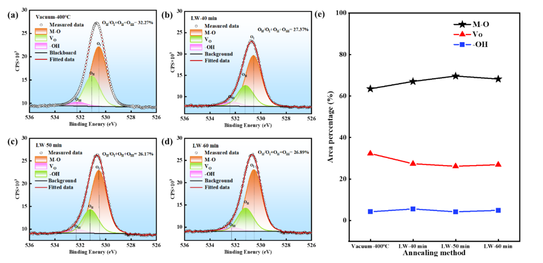
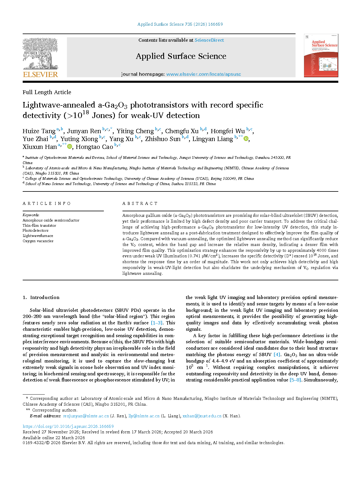
Fig. 1. XPS analysis of a-Ga2O3 films under varied annealing conditions.(a–d) O 1s XPS spectra for samples: (a) vacuum-400 ◦C, (b) LW-40 min, (c) LW-50 min, and (d) LW-60 min. (e) Quantitative area percentage of M–O, VO, and –OH components across annealing methods, extracted from XPS spectral deconvolution.
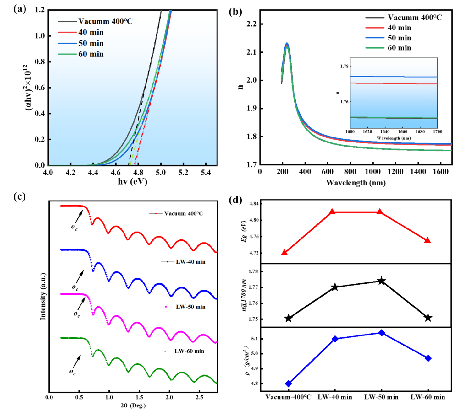
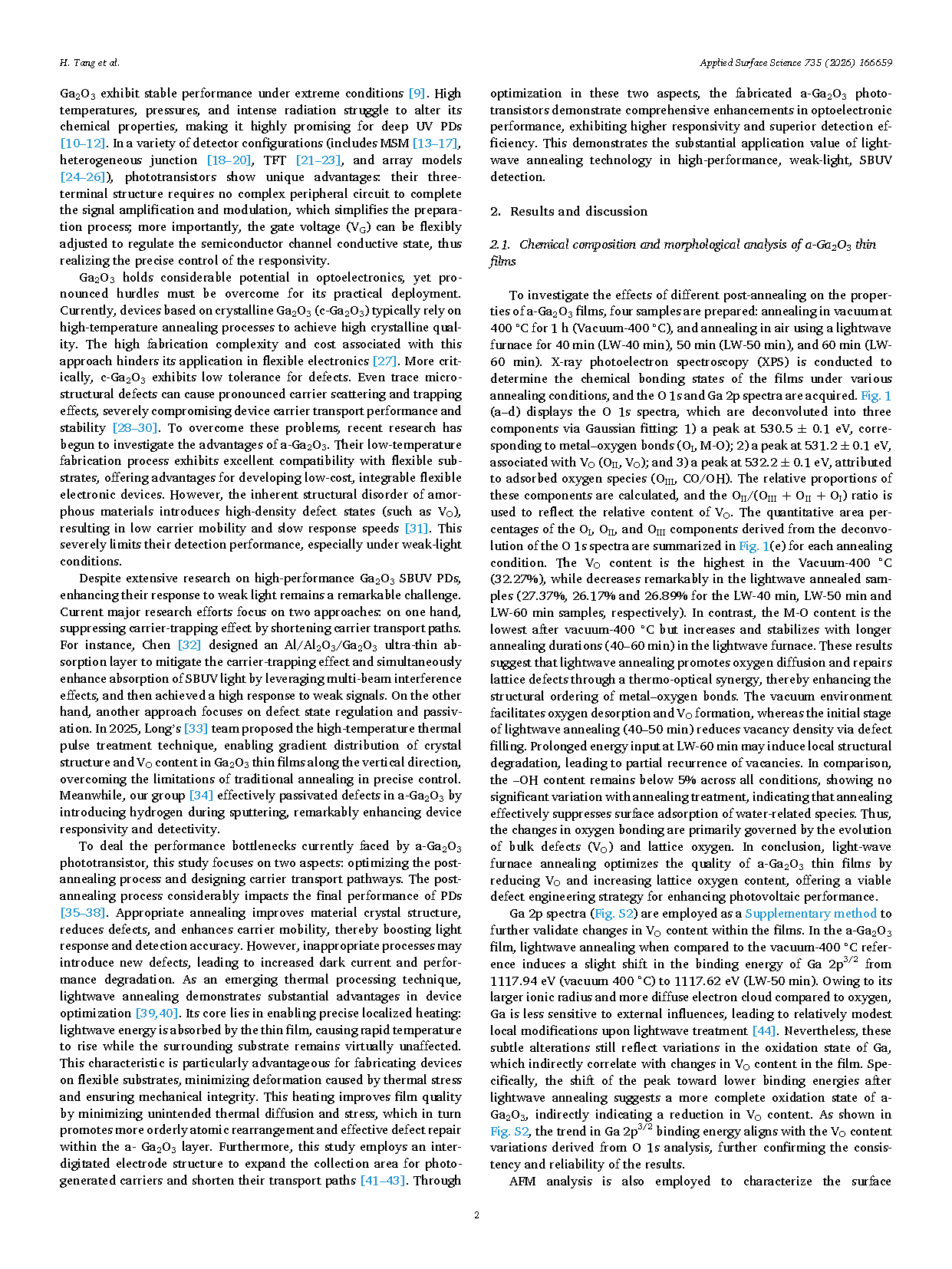
Fig. 2.Optical and structural characterizations of a-Ga2O3 films under different annealing conditions. Curves correspond to vacuum-400 ℃ and LW-40 min, LW-50 min, LW-60 min, respectively. (a) Plots of (αhν)2 versus photon energy (hν), where shows the corresponding band gaps obtained by the Tauc plot method. (b) Refractive index as a function of wavelength for a-Ga2O3 films with different annealing conditions. The inset shows a magnified view of the n at 1700 nm; (c) Magnified view of the XRR spectra, with θc representing the all-external-reflection critical angle. (d) Summary of key optical parameters: Eg(top), n@1700 nm(middle), and ρ(bottom).
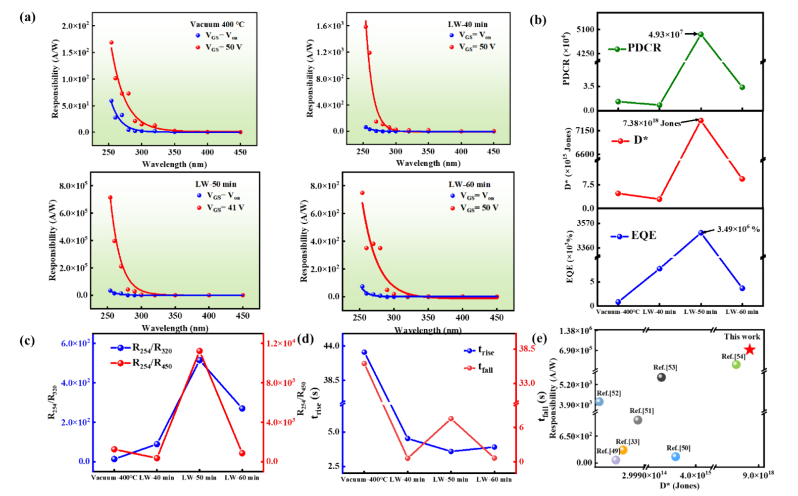
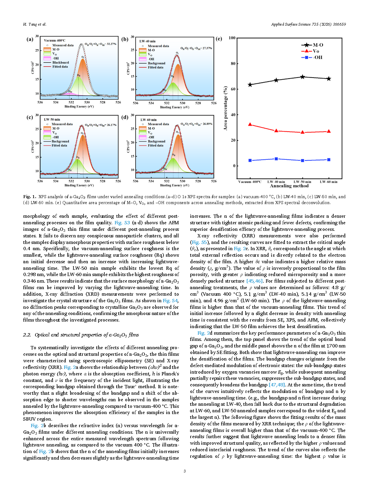
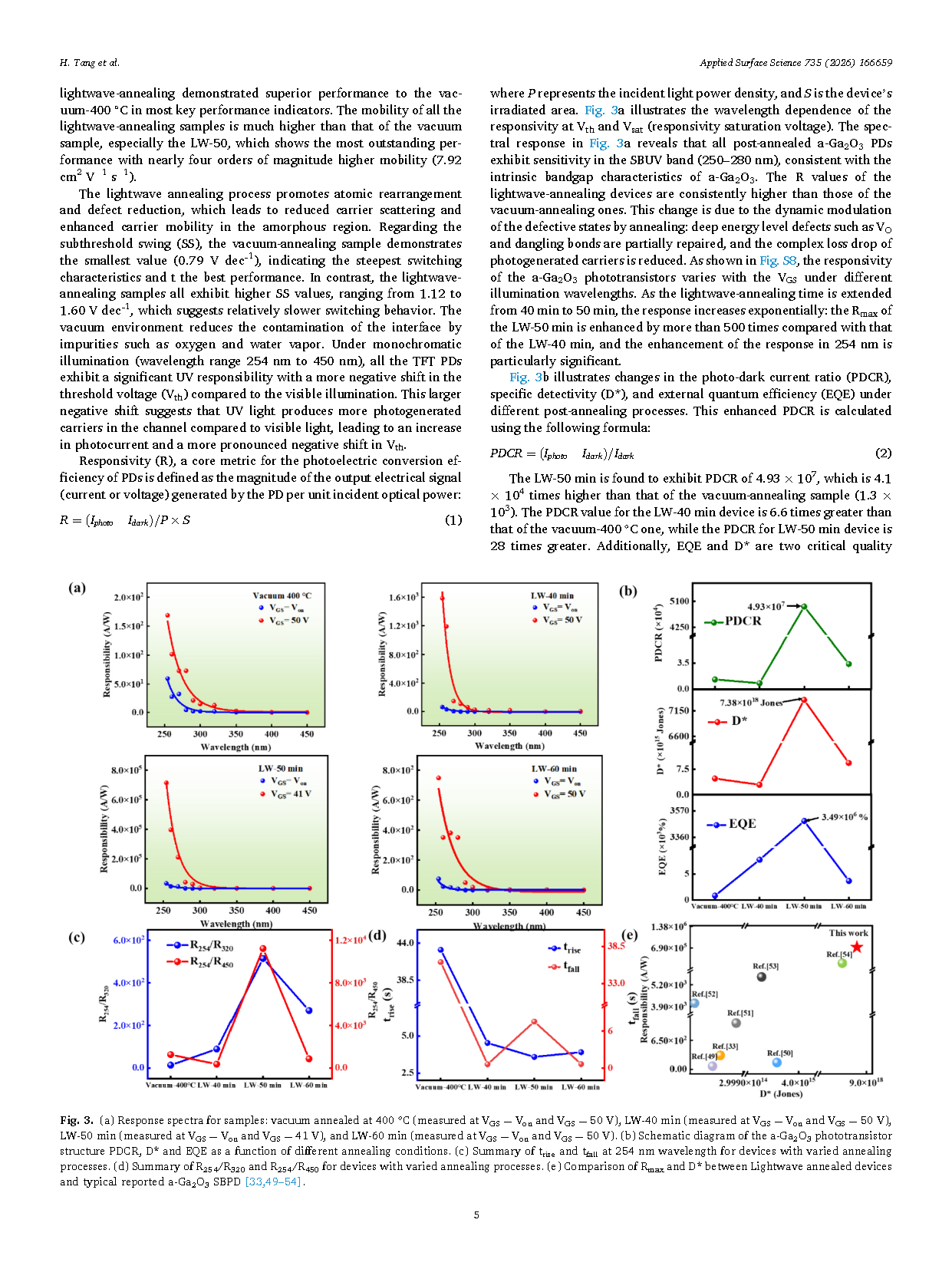
Fig. 3. (a)Response spectra for samples: vacuum annealed at 400 ℃ (measured at VGS =Von and VGS =50 V) , LW-40 min (measured at VGS =Von and VGS =50 V),LW-50 min (measured at VGS =Von and VGS =41 V), and LW-60 min (measured at VGS =Von and VGS) =50 V).(b)Schematic diagram of the a-Ga2O3 phototransistor structure PDCR, D* and EQE as a function of different annealing conditions.(c)Summary of trise and tfall at 254 nm wavelength for devices with varied annealing processes.(d)Summary of R254/R320 and R254/R450 for devices with varied annealing processes.(e)Comparison of Rmax and D* between Lightwave annealed devices and typical reported a-Ga2O3 SBPD.
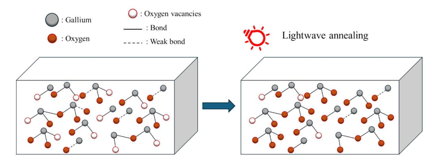
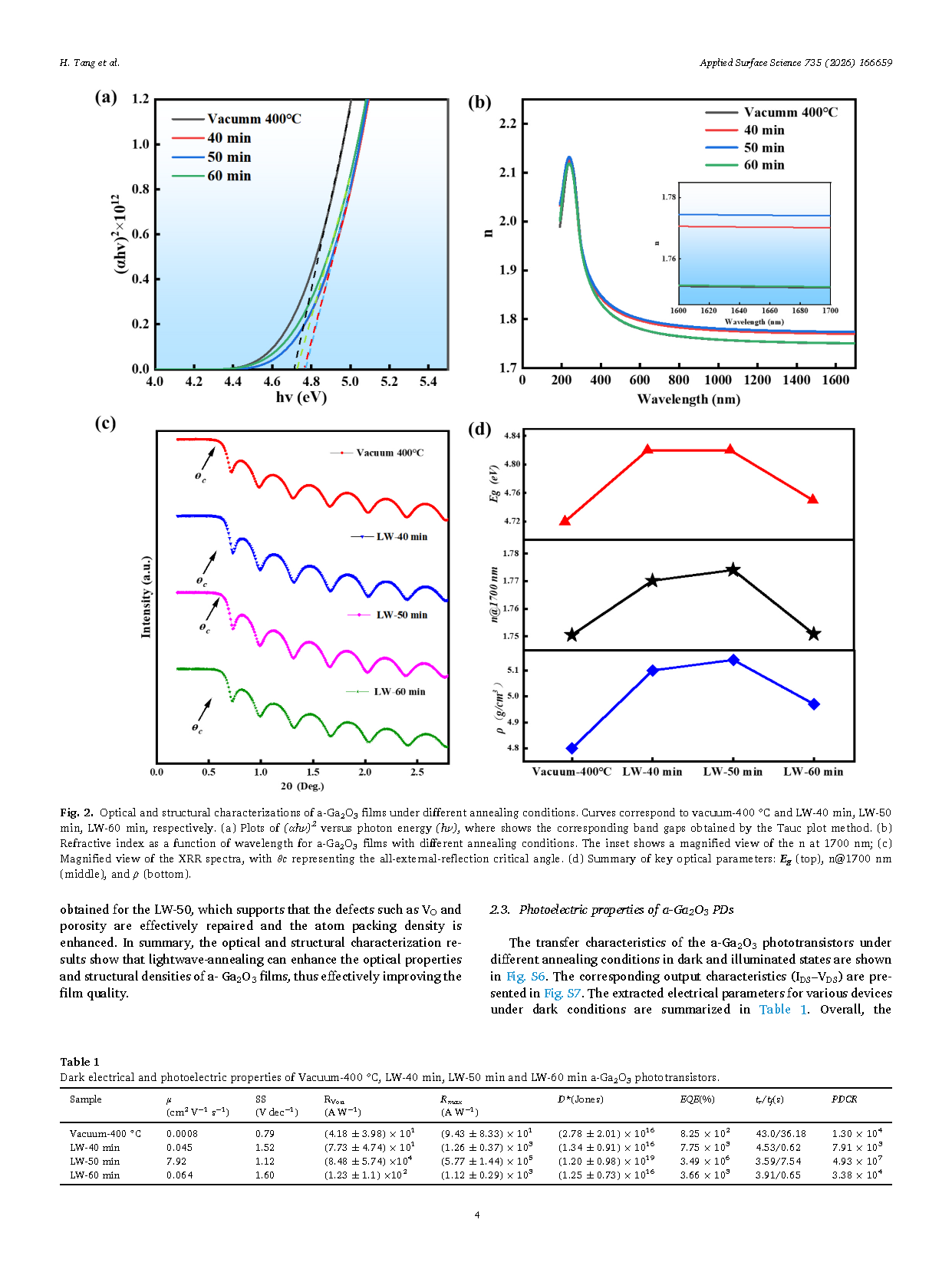
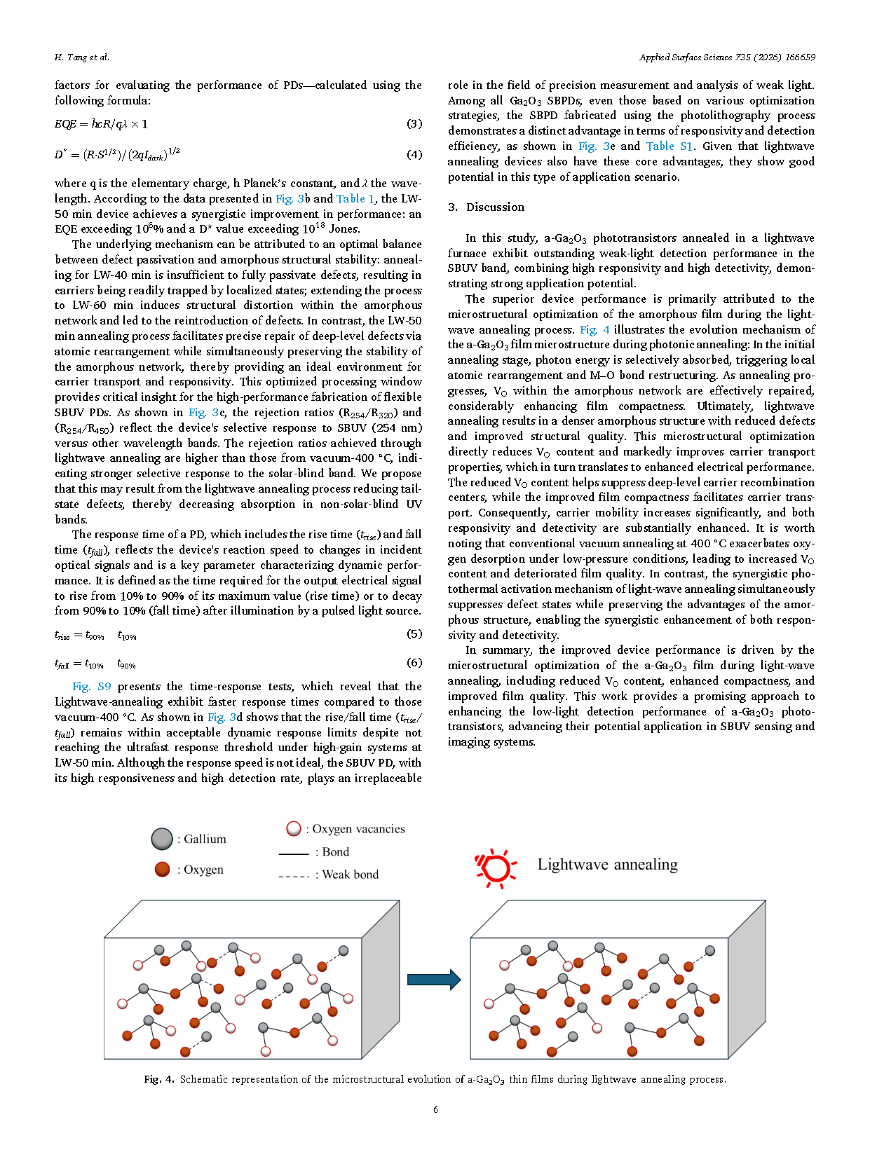
Fig. 4. Schematic representation of the microstructural evolution of a-Ga2O3 thin films during lightwave annealing process.
DOI:
doi.org/10.1016/j.apsusc.2026.166659