Paper Sharing
【Member Papers】UV NIR Dual Band Heterojunction Photodetector Based on p-InP/Ga₂O₃ with Oxygen Vacancy Engineering
日期:2026-04-14阅读:198
Researchers from Tianjin University of Technology have published a dissertation titled “UV NIR Dual Band Heterojunction Photodetector Based on p-InP/Ga₂O₃ with Oxygen Vacancy Engineering” in Materials Science in Semiconductor Processing.
Background
Photodetectors are core optoelectronic devices converting optical signals into electrical signals, widely used in imaging, optical communication, remote sensing and defense.
UV band has extremely low background noise while NIR band owns abundant bandwidth, making UV‑NIR dual‑band detection highly desirable for miniaturized systems.
Traditional dual‑band devices rely on complex techniques (MBE, MOCVD) with high cost and lattice mismatch issues.
Ga2O3 is ideal for UV detection while InP suits NIR detection; their heter-ojunction can realize dual‑band response via low‑cost magnetron sputtering.
Main Contect
In this study, amorphous Ga2O3 thin films were deposited on p-InP substrates using RF magnetron sputtering technology. By synergistically regulating film defects and energy band structures through oxygen vacancy (VO) engineering, p-InP/Ga2O3 heterojunction photodetectors were successfully constructed, achieving self-powered UV-NIR dual-band detection under zero-bias voltage.
Materials and Device Fabrication
Films were sputtered onto p-InP and Al2O3 substrates using a high-purity (99.99%) Ga2O3 target;
Regulate the sputtering atmosphere conditions: “w/o O2”, “w O2”, and “w/o–w O2”;
Ti/Pt electrodes were deposited via magnetron sputtering to complete the heterojunction device fabrication.
Structural and Morphological Characterization
XRD patterns and Raman spectra confirmed that the Ga2O3 thin films possess an amorphous structure;
AFM morphology analysis showed that the introduction of oxygen led to higher film flatness and lower surface root-mean-square(RMS) roughness;
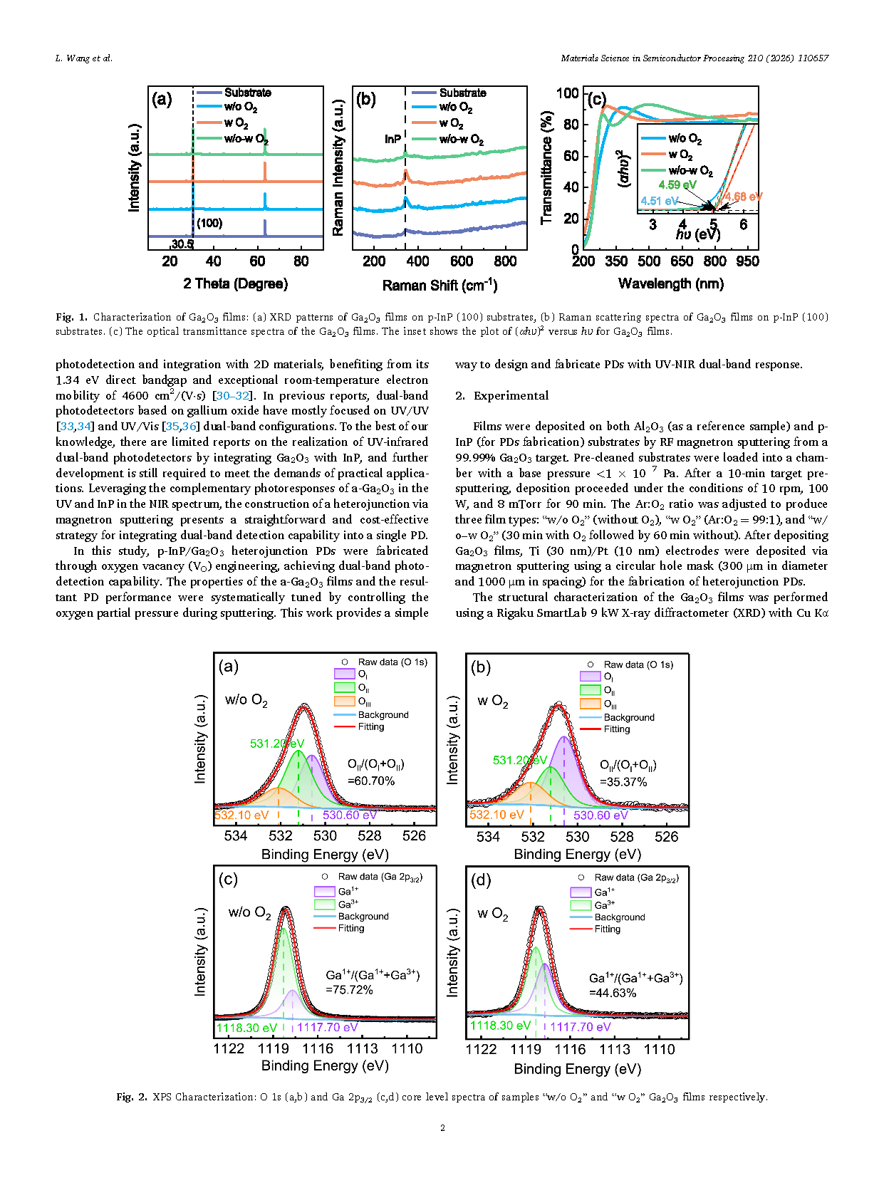
XPS analysis indicated that deposition without oxygen resulted in a higher VO concentration, while the introduction of oxygen significantly reduced the proportion of oxygen vacancy defects.
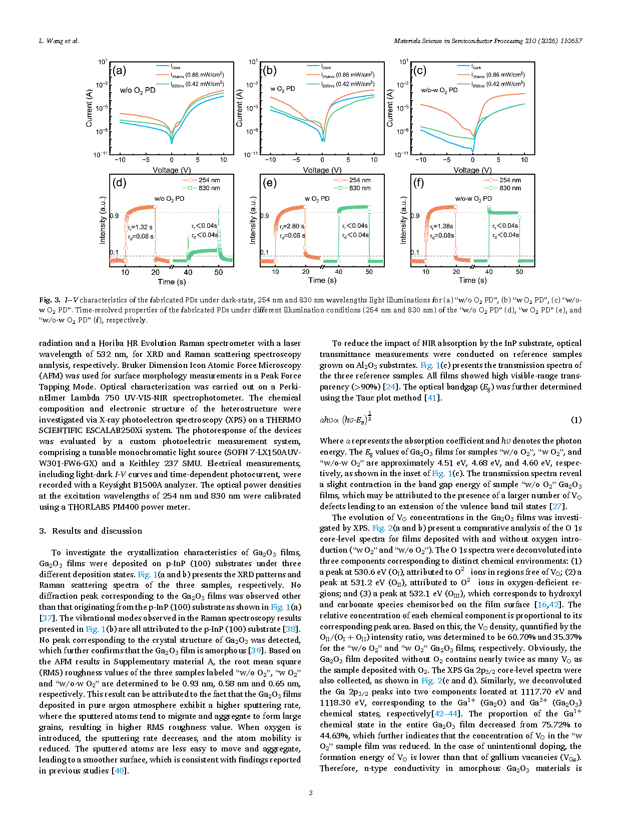
Optoelectronic Performance (Zero Bias)
254 nm ultraviolet: Response rate 0.51 mA/W, Rise time 1.38 s, Fall time 0.08 s;
830 nm near-infrared: Response rate 0.31 mA/W, Rise time/Fall time both < 0.04 s;
The device with the best comprehensive performance is the w/o‑w O2 composite structure, which combines the advantages of low dark current, high rectification ratio and dual-band response.
Mechanism and Application Verification
The heterojunction exhibits a typical Type-I band alignment, where the built-in electric field drives carrier separation, enabling self-powered operation;
Oxygen vacancy engineering effectively regulates carrier concentration and response speed;
The device was successfully applied in an optical communication system utilizing UV and NIR light signals to achieve binary-coded transmission.
Highlight
Material innovation: First combination of p‑InP and amorphous Ga2O3 for single‑device UV‑NIR dual‑band response.
Low‑cost process: Magnetron sputtering instead of MBE/MOCVD, simple, low‑cost and scalable.
Precise VO tuning: Staged deposition balances vacancy concentration, improving responsivity and suppressing dark current.
Self‑powered communication: Zero‑bias operation enables UV‑NIR dual‑channel secure optical communication.
Conclusion
We successfully fabricated p‑InP/Ga2O3 heterojunction photodetectors via oxygen vacancy engineering and low‑cost magnetron sputtering, achieving zero‑bias UV‑NIR dual‑band self‑powered detection. The device shows good performance at 254 nm and 830 nm with high on/off ratio and fast speed. It has been verified in dual‑band optical communication, providing a new route for low‑cost, miniaturized dual‑band photodetectors.
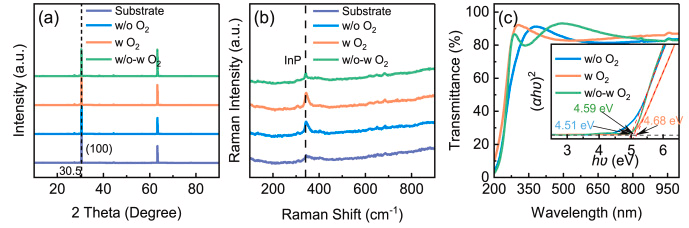
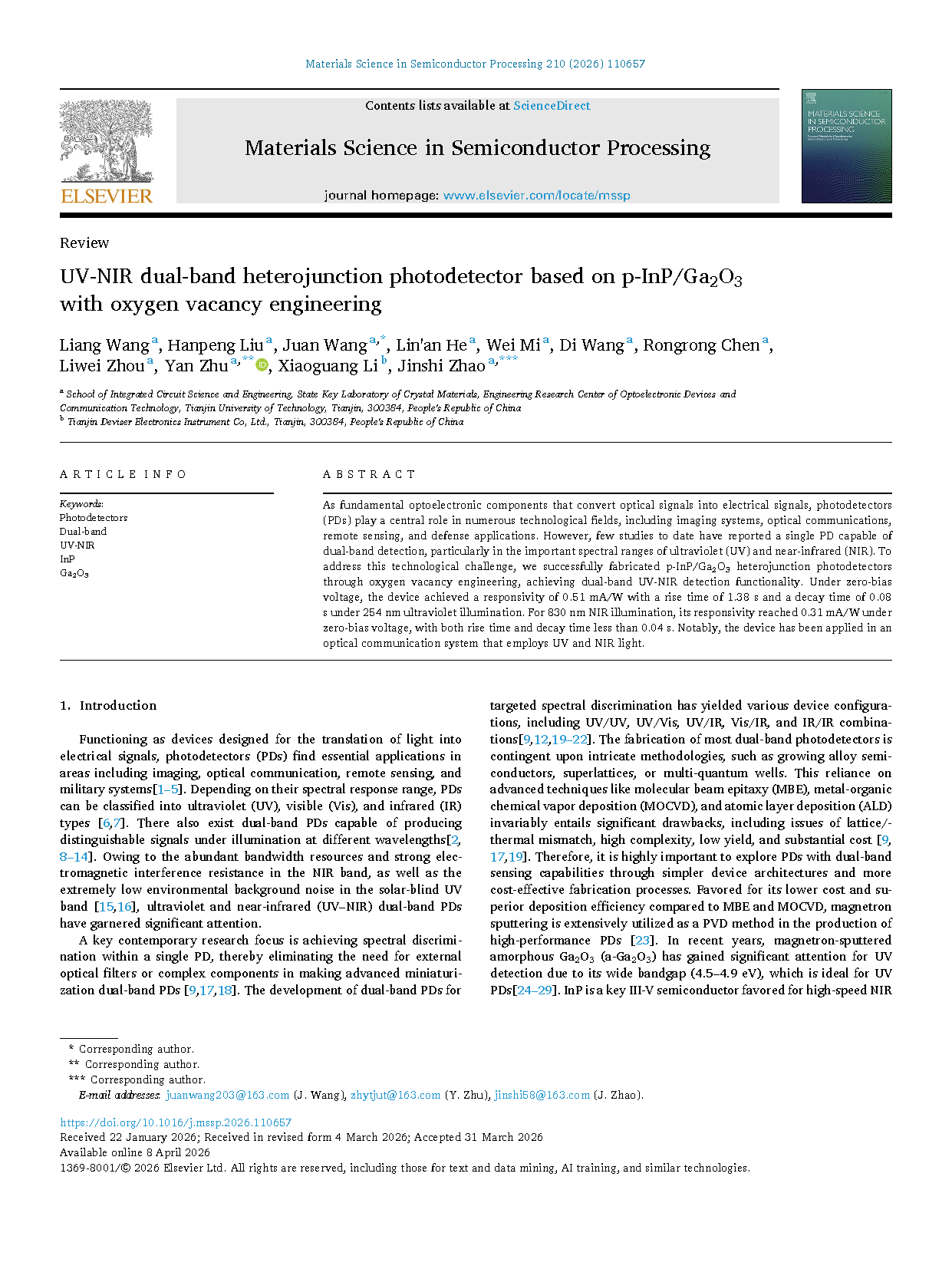
Fig. 1. Characterization of Ga2O3 films: (a) XRD patterns of Ga2O3 films on p-InP (100) substrates, (b) Raman scattering spectra of Ga2O3 films on p-InP (100) substrates. (c) The optical transmittance spectra of the Ga2O3 films. The inset shows the plot of (αhʋ)2 versus hʋ for Ga2O3 films.
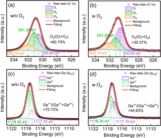
Fig. 2. XPS Characterization: O 1s (a,b) and Ga 2p3/2 (c,d) core level spectra of samples “w/o O2” and “w O2” Ga2O3 films respectively.
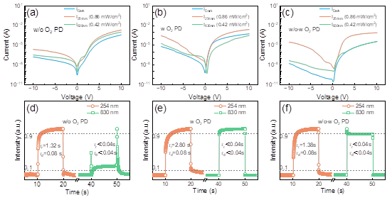
Fig. 3. I−V characteristics of the fabricated PDs under dark-state, 254 nm and 830 nm wavelengths light illuminations for (a) “w/o O2 PD”, (b) “w O2 PD”, (c) “w/o-w O2 PD”. Time-resolved properties of the fabricated PDs under different illumination conditions (254 nm and 830 nm) of the “w/o O2 PD” (d), “w O2 PD” (e), and “w/o-w O2 PD” (f), respectively.
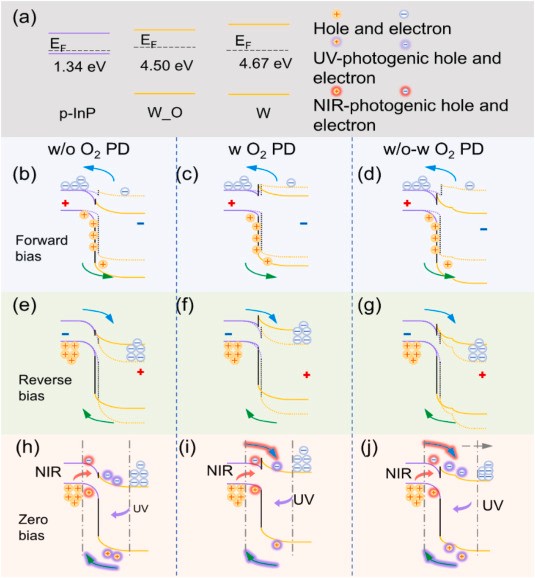
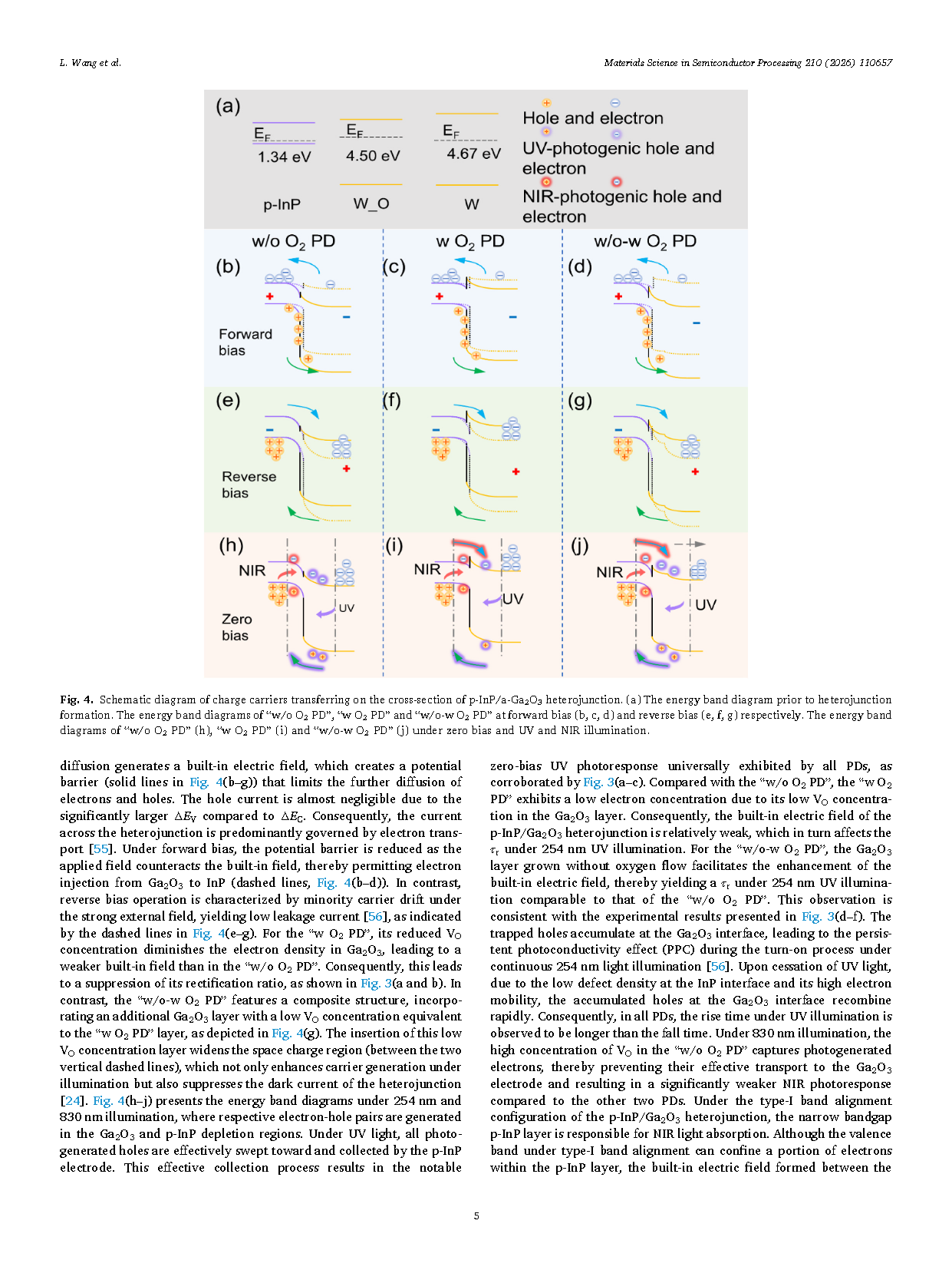
Fig. 4. Schematic diagram of charge carriers transferring on the cross-section of p-InP/a-Ga2O3 heterojunction. (a) The energy band diagram prior to heterojunction formation. The energy band diagrams of “w/o O2 PD”, “w O2 PD” and “w/o-w O2 PD” at forward bias (b, c, d) and reverse bias (e, f, g) respectively. The energy band diagrams of “w/o O2 PD” (h), “w O2 PD” (i) and “w/o-w O2 PD” (j) under zero bias and UV and NIR illumination.
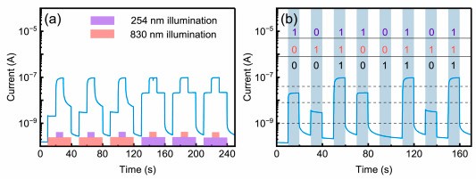
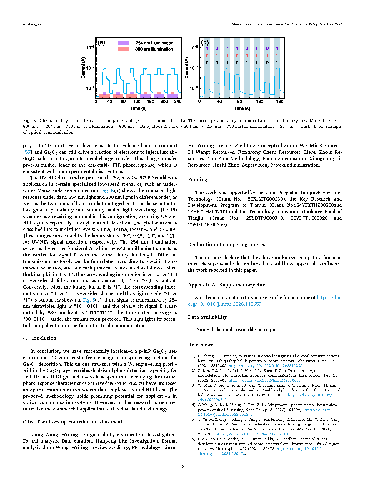
Fig. 5. Schematic diagram of the calculation process of optical communication. (a) The three operational cycles under two illumination regimes: Mode 1: Dark → 830 nm → (254 nm + 830 nm) co-illumination → 830 nm → Dark; Mode 2: Dark → 254 nm → (254 nm + 830 nm) co-illumination → 254 nm → Dark. (b) An example of optical communication.
DOI:
doi.org/10.1016/j.mssp.2026.110657