Paper Sharing
【International Papers】Polycrystalline κ-Ga₂O₃ on Si(100) substrates with GZO buffer layers
日期:2026-04-15阅读:155
Researchers from Kyoto Institute of Technology, Kochi University of Technology, Kanazawa Institute of Technology, Meiji University have published a dissertation titled “Polycrystalline κ‑Ga₂O₃ on Si(100) substrates with GZO buffer layers” in RSC Advances.
Background
κ‑Ga₂O₃ is an emerging piezoelectric semiconductor with promising applications in radio‑frequency devices. However, heteroepitaxial growth of κ‑Ga₂O₃ on silicon substrates is challenging due to large lattice mismatch and interfacial oxidation. Conventional epitaxial methods rely on single‑crystal buffer layers such as AlN and Mo. For practical piezoelectric devices, crystallographic isotropy is critical for design flexibility. This study first realizes polycrystalline κ‑Ga₂O₃ growth on Si(100) using a GZO buffer layer, which features a simpler process and isotropic film properties suitable for Si‑based integration.
Abstract
Kappa-phase gallium oxide (κ‑Ga₂O₃) is an emerging piezoelectric semiconductor with potential applications in radio-frequency devices. However, heteroepitaxial growth of κ‑Ga₂O₃ on silicon substrates remains challenging owing to large lattice mismatch and interfacial oxidation. This study demonstrates the growth of polycrystalline κ‑Ga₂O₃ thin films deposited by mist chemical vapor deposition (mist CVD) on Si(100) substrates using Ga-doped ZnO (GZO) buffer layers. Structural characterization via X-ray diffraction, scanning electron microscopy, and transmission electron microscopy reveals that κ‑Ga₂O₃ films exhibit a c-axis oriented polycrystalline structure with random in-plane orientations, which yields isotropic properties that are advantageous for device applications. A ZnGa₂O₄ intermediate layer is identified at the κ‑Ga₂O₃/GZO interface, which plays a critical role in phase stabilization. These findings indicate that polycrystalline κ‑Ga₂O₃ on Si substrates represents a promising platform for piezoelectric semiconductor devices.
Highlights
First demonstration of phase-pure polycrystalline κ‑Ga₂O₃ on Si(100) using a polycrystalline GZO buffer layer, replacing conventional single‑crystal buffers such as AlN/Mo.
The film shows c‑axis preferred orientation with random in‑plane grains, achieving excellent isotropy beneficial for piezoelectric device design.
In‑situ formation of ZnGa₂O₄ interlayer at the interface effectively stabilizes the κ‑phase and suppresses secondary phases.
Mist CVD process under atmospheric pressure and low temperature features low cost and high compatibility with Si‑based CMOS technology
Conclusion
In this study, we successfully demonstrated the growth of polycrystalline κ‑Ga₂O₃ thin films deposited by mist CVD on Si(100) substrates using GZO buffer layers. The c-axis-oriented GZO buffer layer promotes the formation of κ‑Ga₂O₃ due to its hexagonal oxygen atomic arrangement. Furthermore, the presence of amorphous SiO₂ on the Si substrate prevents the establishment of an epitaxial relationship in the κ‑Ga₂O₃/GZO/Si structure, resulting in the polycrystalline growth of κ‑Ga₂O₃. Unlike previous studies employing epitaxial buffer layers such as AlN or Mo, the use of a polycrystalline GZO buffer layer provides a simpler growth process and inherently isotropic film properties, making it a more practical approach for integrating κ‑Ga₂O₃-based piezoelectric devices with Si technology. Structural analysis revealed that the κ‑Ga₂O₃ films exhibit random crystallographic orientations, which inherently provide isotropic properties that are advantageous for piezoelectric device applications. The formation of a ZnGa₂O₄ intermediate layer at the κ‑Ga₂O₃/GZO interface was identified as a key factor in stabilizing the k-phase. Unlike conventional epitaxial κ‑Ga₂O₃ films with ordered rotational domains, the polycrystalline nature of our films offers more complete isotropy and potentially simplifies the growth process on technologically important Si substrates. These results open new possibilities for integrating κ‑Ga₂O₃-based piezoelectric devices with silicon technology. Further optimization of the growth conditions and buffer layer engineering can potentially enable high-performance piezoelectric applications of polycrystalline κ‑Ga₂O₃ thin films.
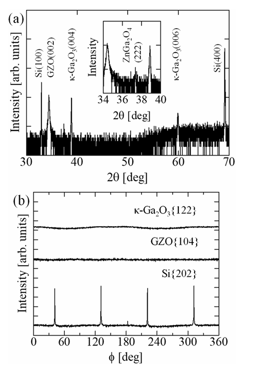
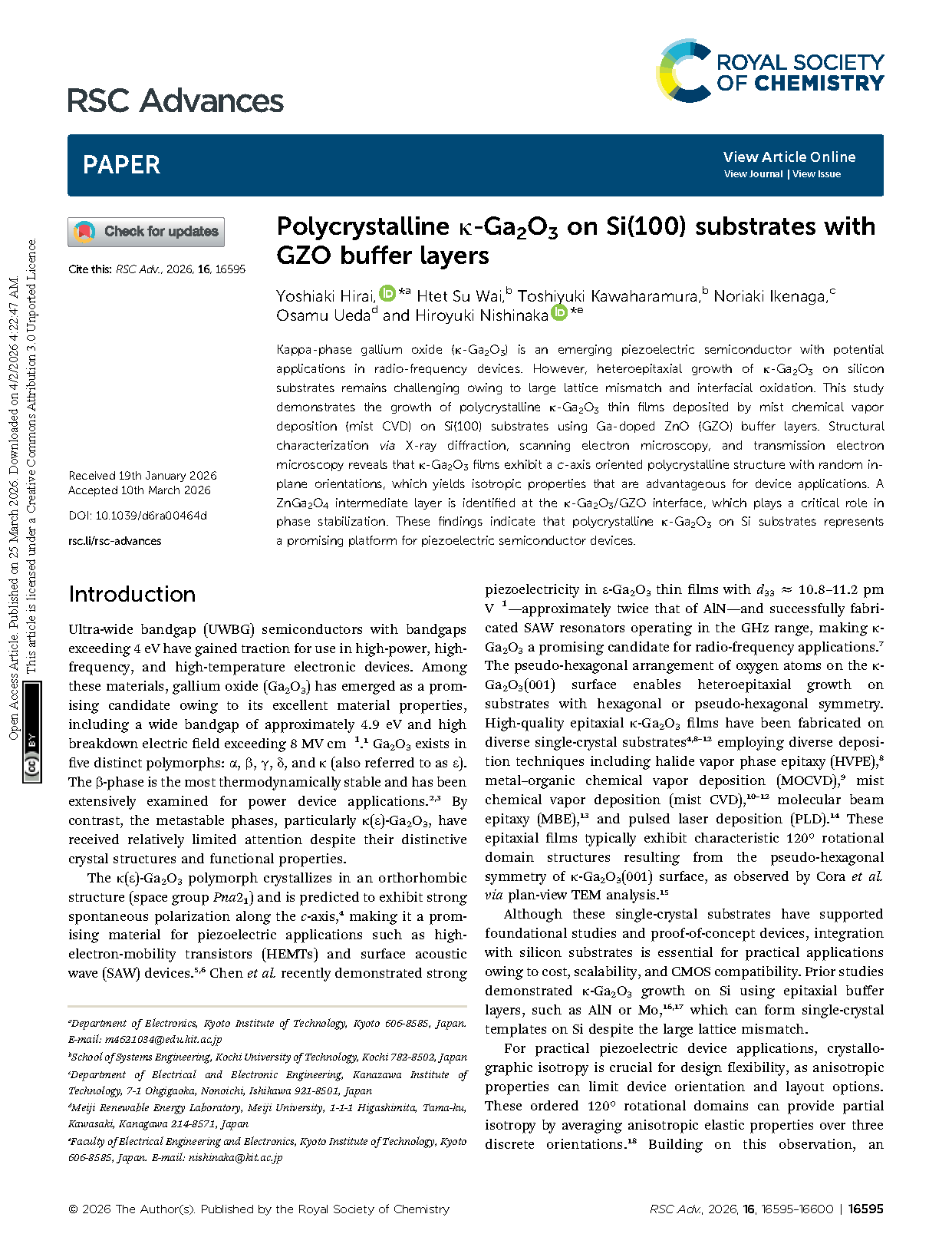
Figure 1 (a) XRD 2θ–ω scan of κ‑Ga₂O₃ grown on GZO/Si. (b) XRD φ‑scan of three layers.
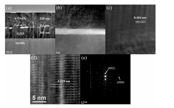
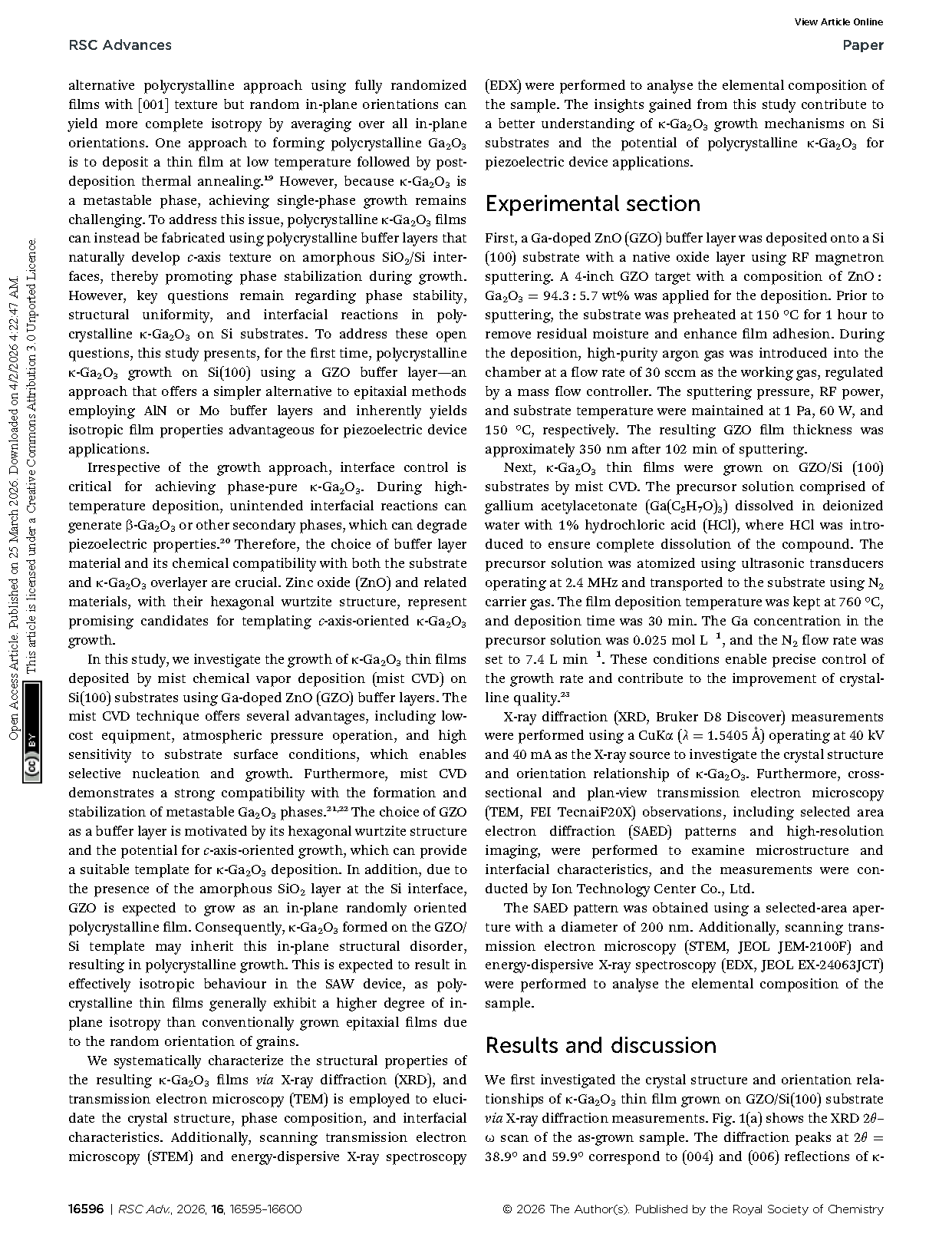
Figure 2 (a) Cross‑sectional TEM image of κ‑Ga₂O₃/GZO/Si(100) structure. (b) High‑resolution TEM images of the GZO/Si interface, (c) ZnGa₂O₄ interlayer, and (d) κ‑Ga₂O₃ film. (e) SAED pattern obtained from κ‑Ga₂O₃ layer in cross‑sectional view.
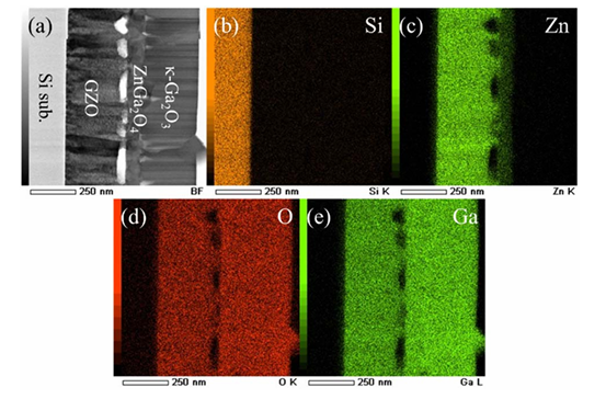
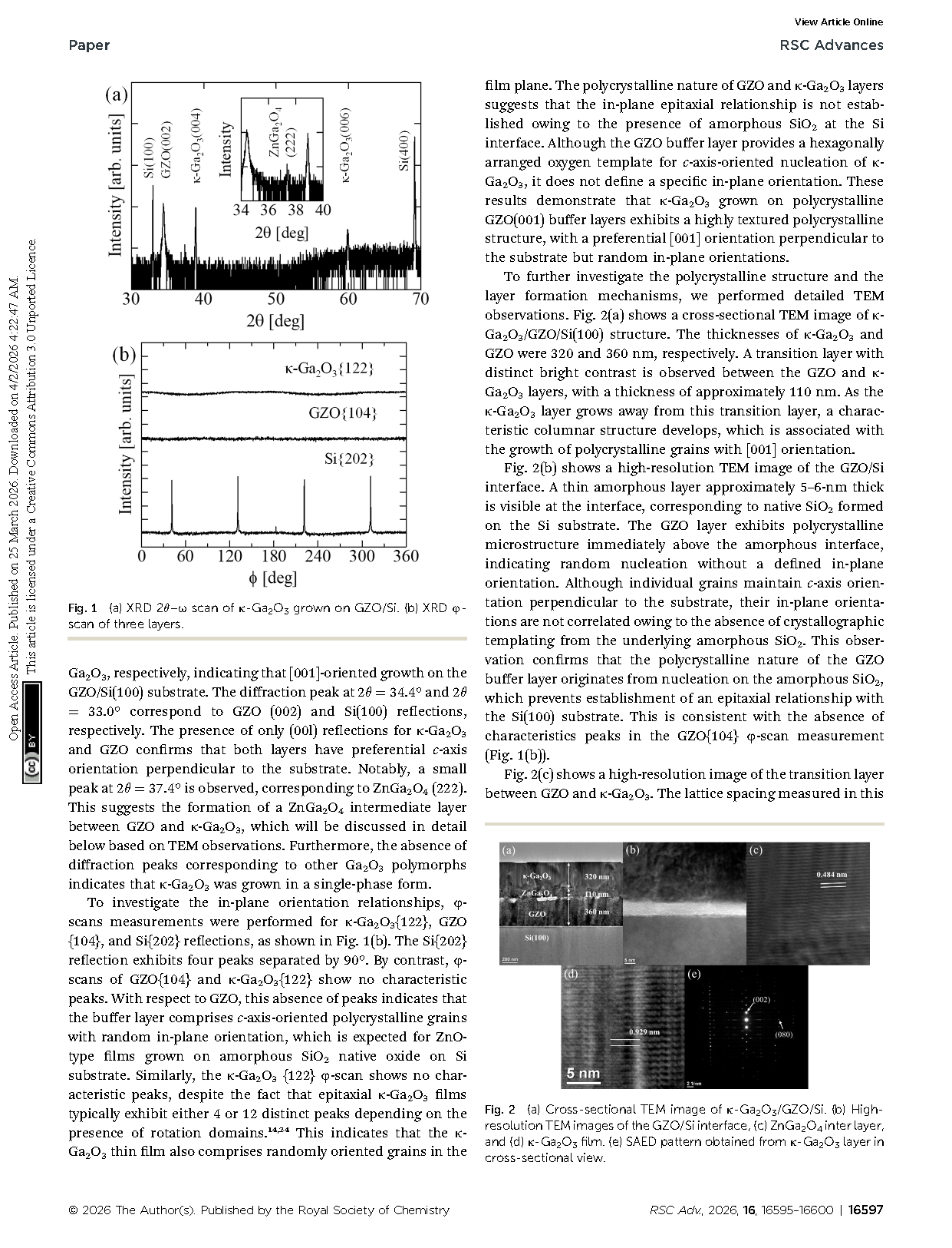
Figure 3 (a) STEM image of κ‑Ga₂O₃/GZO/Si (b)–(e) Elemental mapping showing the dispersion of Si, Zn, O, Ga.
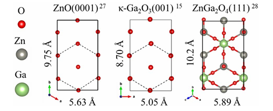
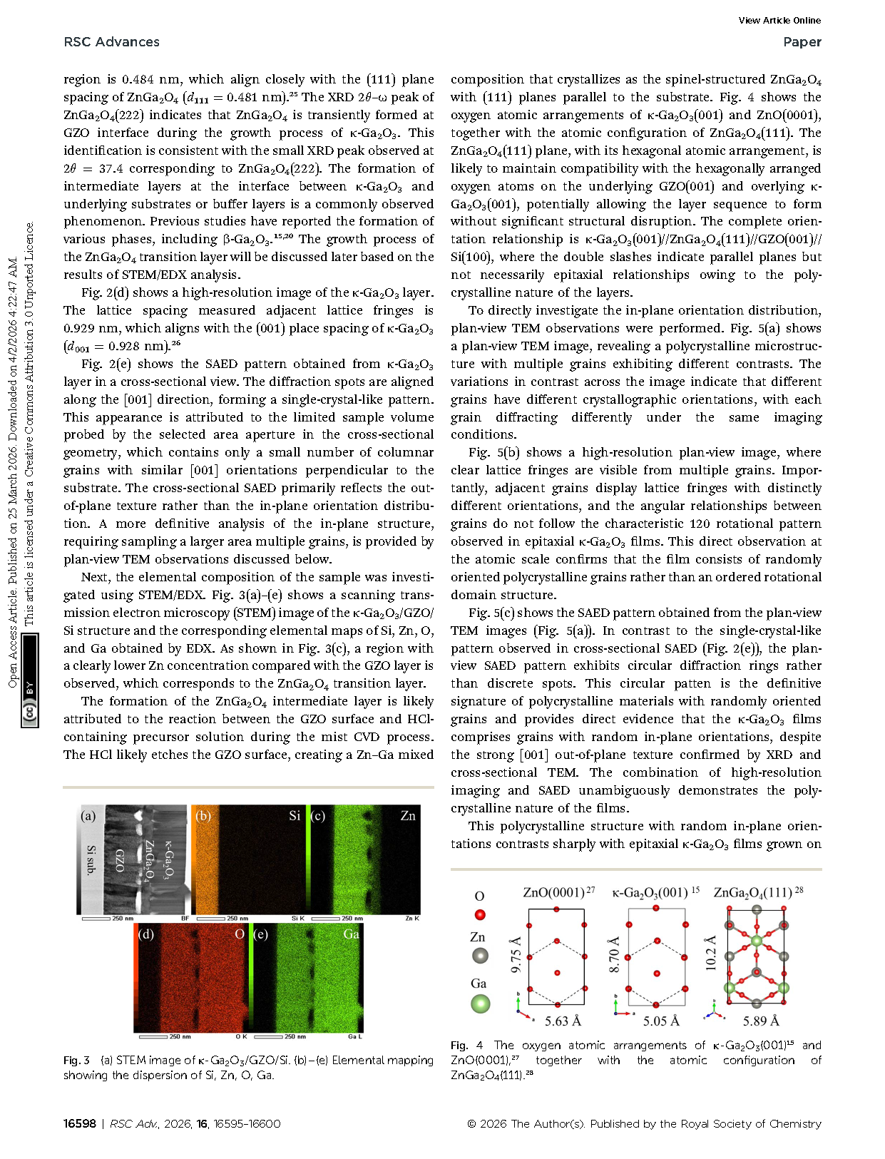
Figure 4 The oxygen atomic arrangements of κ‑Ga₂O₃(001) and ZnO(0001), together with the atomic configuration of ZnGa₂O₄(111).
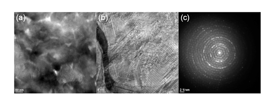
Figure 5 (a) Plan‑view TEM image of κ‑Ga₂O₃ film. (b) High‑resolution plan‑view TEM image of κ‑Ga₂O₃. (c) SAED pattern obtained from the plan‑view TEM image.
DOI:
doi.org/10.1039/D6RA00464D