Paper Sharing
【Domestic Papers】Ga₂O₃ Deep-Ultraviolet Photodetectors: Materials, Device Architectures, and Performance Frontiers
日期:2026-04-15阅读:212
Researchers from the University of Chinese Academy of Sciences have published a dissertation titled "Ga₂O₃ Deep-Ultraviolet Photodetectors: Materials, Device Architectures, and Performance Frontiers" in ACS Applied Electronic Materials.
Background
Deep-ultraviolet (DUV) photodetectors operating in the solar-blind region (200−280 nm) are of critical importance for defense, space exploration, environmental monitoring, flame detection, and secure optical communication. Silicon-based photodetectors are unsuitable for solar-blind DUV detection due to narrow bandgap. Among ultrawide-bandgap semiconductors, gallium oxide (Ga₂O₃) has emerged as a leading material platform owing to its large intrinsic bandgap, visible-blind response, high breakdown electric field, and compatibility with scalable growth technologies. Ga₂O₃ is a polymorphic material, and β-Ga₂O₃ is the most thermodynamically stable phase for device applications. However, challenges remain in achieving simultaneous ultrahigh responsivity and fast temporal response, controlling oxygen vacancies and hole trapping, and realizing industrial-scale fabrication.
Abstract
Deep-ultraviolet (DUV) photodetectors operating in the solar-blind region (200−280 nm) are of critical importance for defense, space exploration, environmental monitoring, flame detection, and secure optical communication. Among ultrawide-bandgap semiconductors, gallium oxide (Ga₂O₃) has emerged as a leading material platform owing to its large intrinsic bandgap, visible-blind response, high breakdown electric field, and compatibility with scalable growth technologies. This review provides a comprehensive and structured analysis of Ga₂O₃-based DUV photodetectors, covering nanostructured devices, metal−semiconductor−metal architectures, junction-based photodiodes, avalanche photodetectors, and field-effect-transistor-based photodetectors. Emphasis is placed on structure−property−performance relationships, underlying physical mechanisms, and key trade-offs governing responsivity, detectivity, gain, and response speed.
Highlights
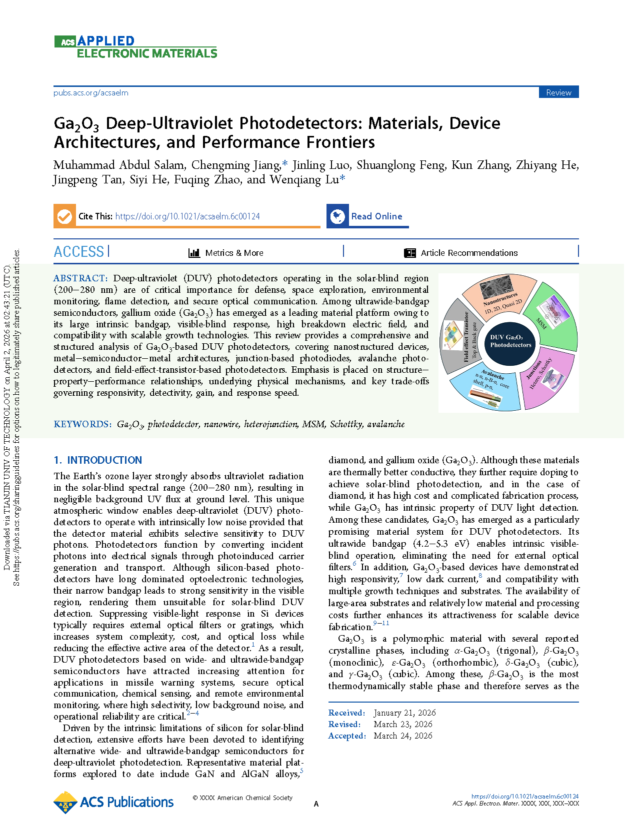
Systematically classify β-Ga₂O₃ DUV photodetectors into five typical device architectures: nanostructured, MSM, junction-based, avalanche, and FET-based photodetectors.
Clarify the structure−property−performance relationships and intrinsic trade-offs between responsivity, response speed, noise and stability for different device configurations.
Summarize the gain mechanisms of various β-Ga₂O₃ photodetectors, including surface trap-assisted gain, built-in electric field separation, avalanche impact ionization and gate-controlled photogating effect.
Point out the key challenges including defect control, p-type doping difficulty, scalable fabrication and propose future directions for balanced performance optimization.
Conclusion
This review has comprehensively surveyed recent advances in β-Ga₂O₃-based deep-ultraviolet photodetectors across a broad range of device architectures, including nanostructured photodetectors, metal−semiconductor−metal devices, junction-based photodiodes, avalanche photodetectors, and field-effect-transistor photodetectors. The growing interest in β-Ga₂O₃ photodetectors is driven by their intrinsic solar-blind response, low dark current, and suitability for applications in communication, imaging, and harsh-environment sensing relevant to both civilian and defense technologies. A central conclusion emerging from this Perspective is that photodetector performance is fundamentally governed by the underlying gain mechanism and device architecture rather than by material choice alone. Nanostructured devices and FET-based photodetectors achieve ultrahigh responsivity primarily through surface-state-assisted or gate-controlled photogating effects, while MSM and junction-based photodetectors emphasize interface-controlled carrier separation, offering improved stability, faster response, and self-powered operation. Avalanche photodetectors represent a distinct regime in which electric-field-driven impact ionization enables high internal gain with a comparatively fast temporal response and reduced reliance on surface trapping. Despite significant progress, optimizing β-Ga₂O₃ photodetectors remains a multidimensional challenge due to intrinsic trade-offs among responsivity, response speed, noise, operating voltage, and device stability. For example, while FET photodetectors can deliver record-high responsivity through gate modulation, such performance often comes at the expense of response speed and long-term stability. In contrast, β-Ga₂O₃ APDs offer a more balanced combination of gain and speed, albeit with the typical requirement of higher operating fields or bias voltages. Several key challenges must be addressed to advance β-Ga₂O₃ photodetectors toward practical deployment. These include precise control of defects and interface states, scalable fabrication of high-quality heterostructures, and the longstanding difficulty of realizing stable p-type β-Ga₂O₃, which currently limits the development of homogeneous junction devices. Progress in interface engineering, dielectric integration, and band-structure design is expected to play a decisive role in overcoming these limitations. Looking forward, the continued development of β-Ga₂O₃ photodetectors will likely benefit from hybrid design strategies that integrate multiple gain and control mechanisms, such as combining junction-based carrier separation with gate modulation or avalanche multiplication. Rather than pursuing isolated performance metrics, future efforts should emphasize balanced optimization tailored to application-specific requirements. With ongoing advances in materials growth and device engineering, β-Ga₂O₃ is well positioned to remain a leading platform for next-generation solar-blind, deep-ultraviolet photonic devices. The slow time response, oxygen defects/surface defects, and industrial reproducibility are the main problems being faced by researchers; many solutions have been tried, such as adding an oxide layer SiO₂ on the substrate and alloy doping of Sn, Ge, and W can possibly solve these issues. Additionally, the structures such as FET photodetectors are less explored and can offer a lot in terms of device performance and optimization.
Project Support
This work was supported by the Chongqing Natural Science Foundation (No. 2025NSCQ-LZX0054) and the Chongqing Natural Science Foundation Innovation and Development Joint Fund (No. CSTB2024NSCQ-LZX0022).
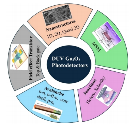
Figure 1 Classification of Ga₂O₃ DUV photodetector device architectures.
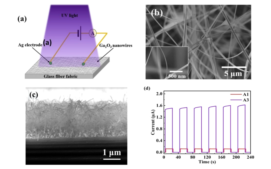
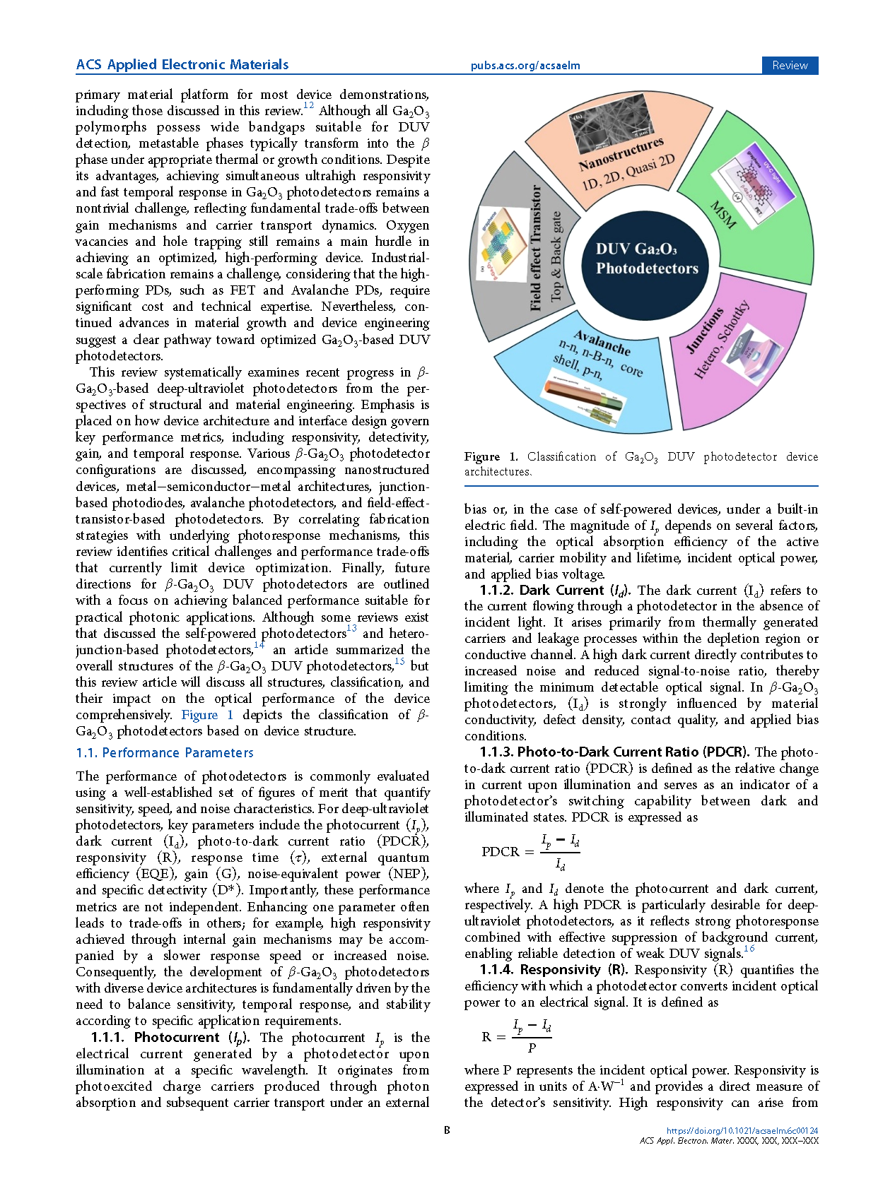
Figure 2 1D β−Ga₂O₃ nanowires. (a) Schematic structure diagram. (b) SEM image with the inset showing an enlarged image. (c) Cross-section SEM image of nanowires. (d) Current−time response of the photodetector.
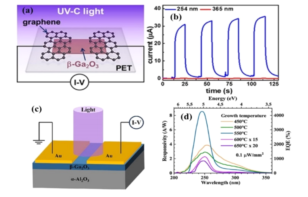
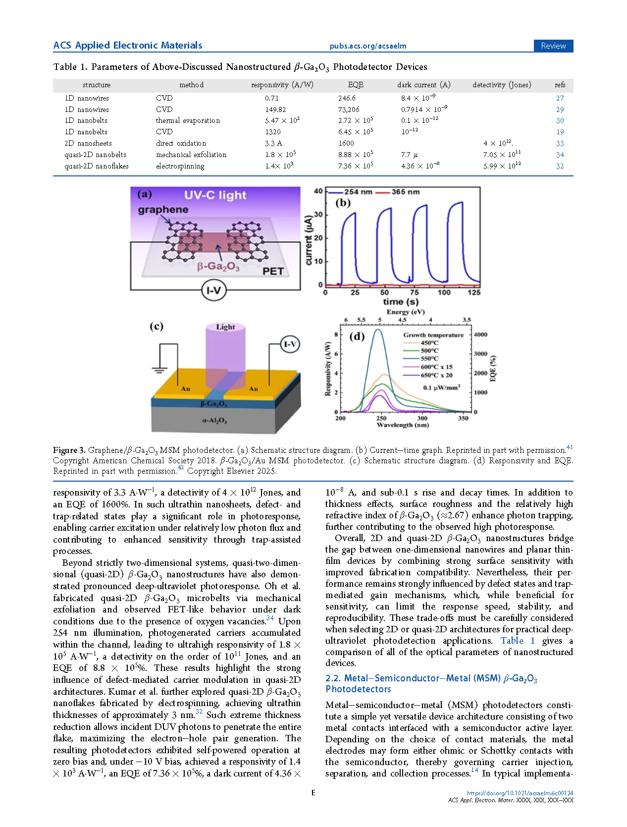
Figure 3 Graphene/β−Ga₂O₃ MSM photodetector. (a) Schematic structure diagram. (b) Current−time graph. β−Ga₂O₃/Au MSM photodetector. (c) Schematic structure diagram. (d) Responsivity and EQE.
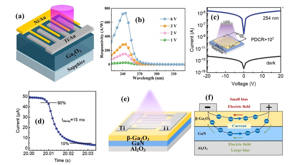
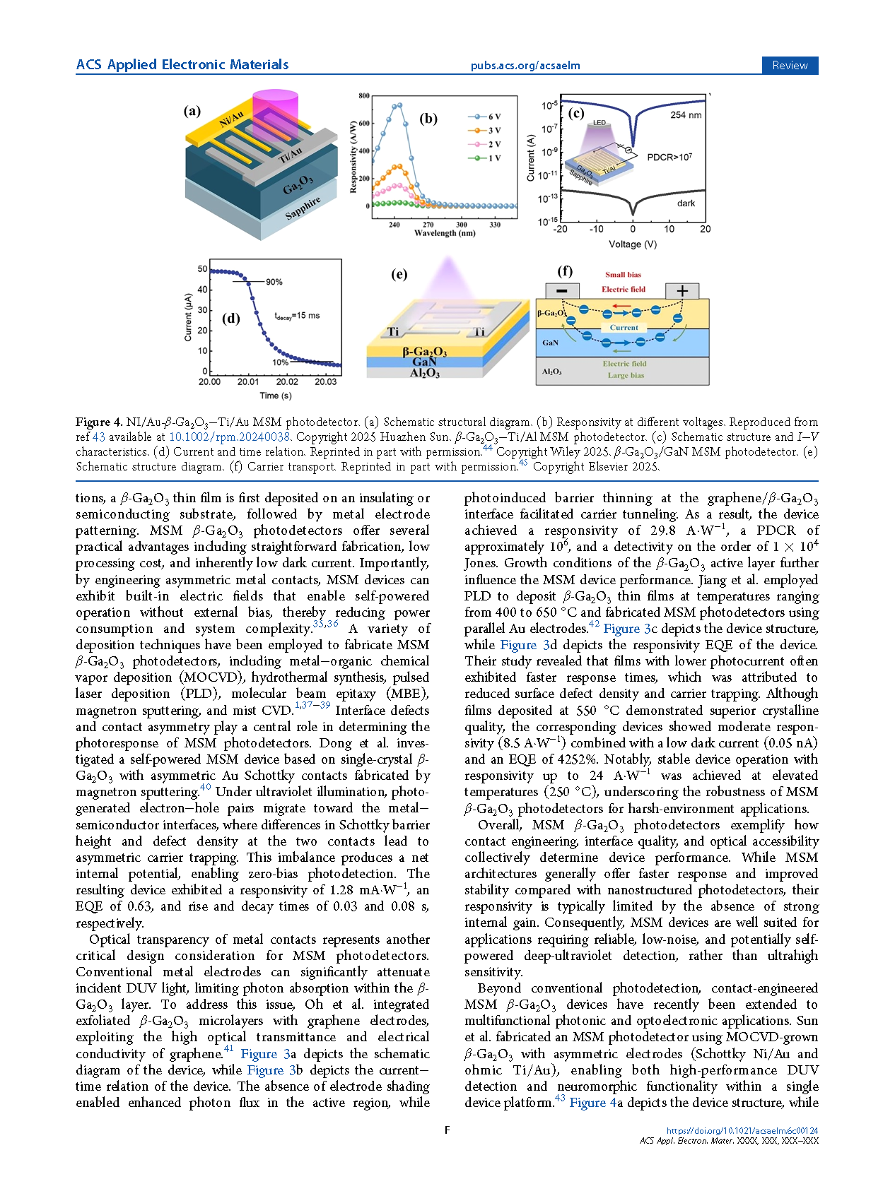
Figure 4 NI/Au-β−Ga₂O₃ Ti/Au MSM photodetector. (a) Schematic structural diagram. (b) Responsivity at different voltages. β−Ga₂O₃−Ti/Al MSM photodetector. (c) Schematic structure and I−V characteristics. (d) Current and time relation. β−Ga₂O₃/GaN MSM photodetector. (e) Schematic structure diagram. (f) Carrier transport.
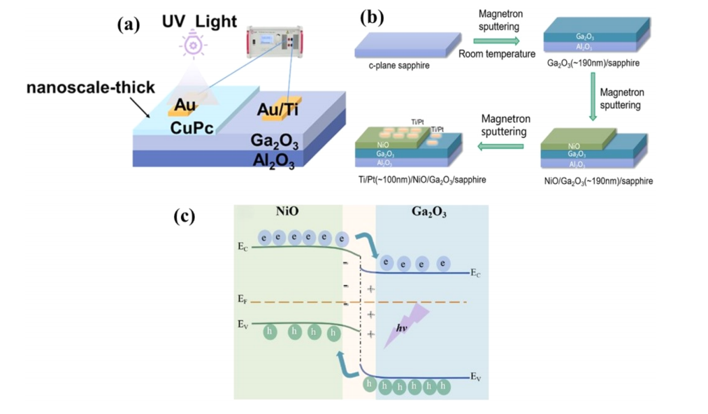
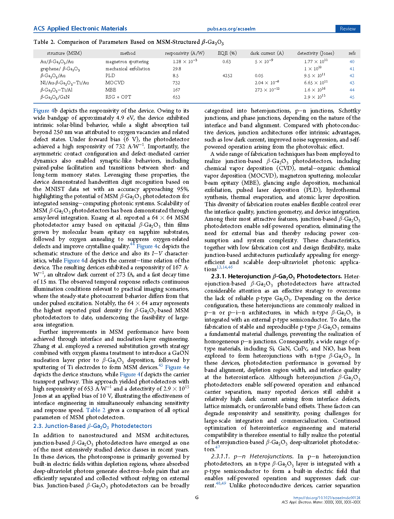
Figure 5 CuPc/β−Ga₂O₃ p−n junction photodetector. (a) Schematic structure. NiO/β−Ga₂O₃ p−n junction photodetector. (b) Synthesis process. (c) Junction under UV light.
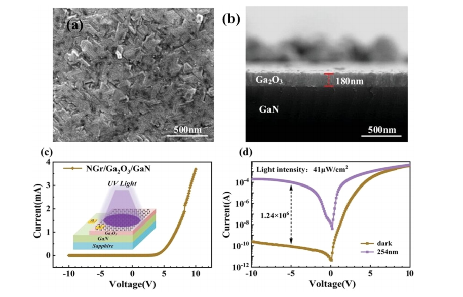
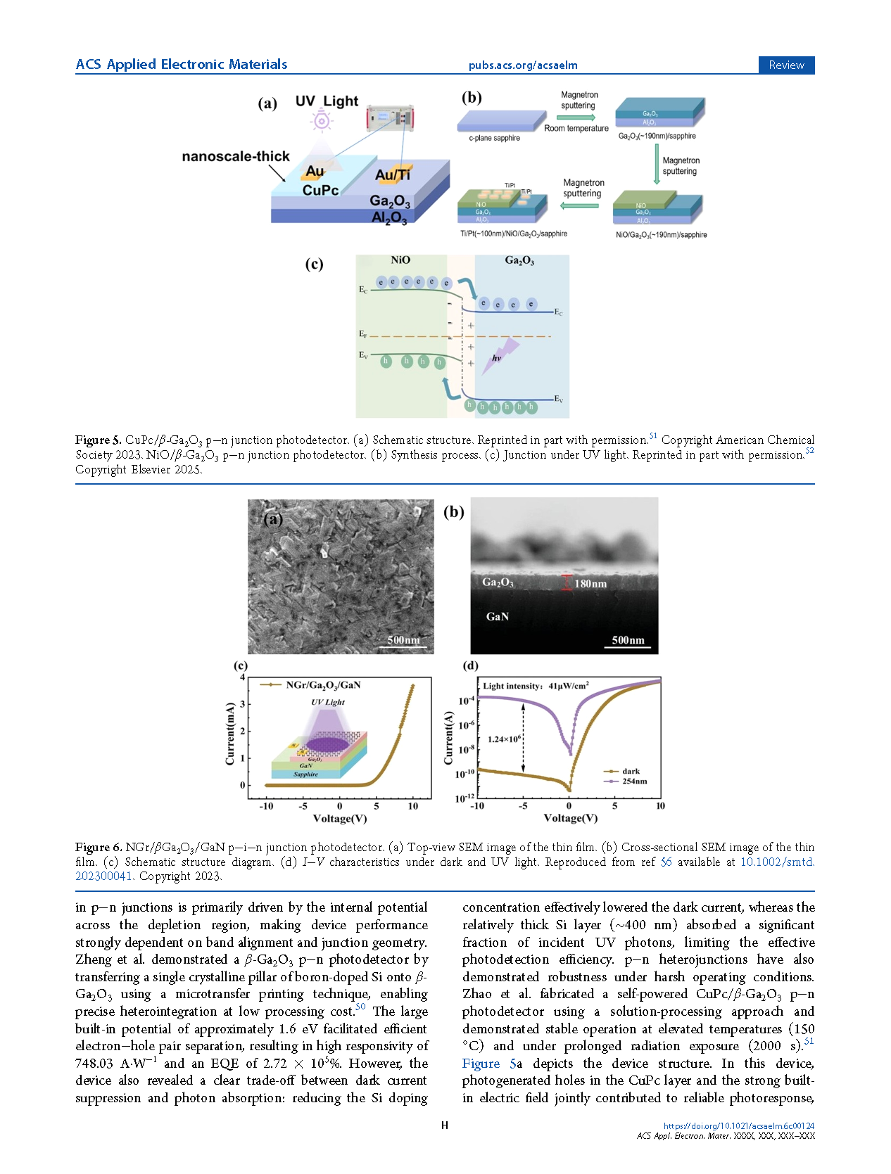
Figure 6 NGr/β−Ga₂O₃/GaN p−i−n junction photodetector. (a) Top-view SEM image of the thin film. (b) Cross-sectional SEM image of the thin film. (c) Schematic structure diagram. (d) I−V characteristics under dark and UV light.
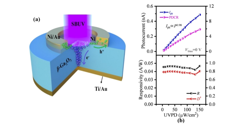
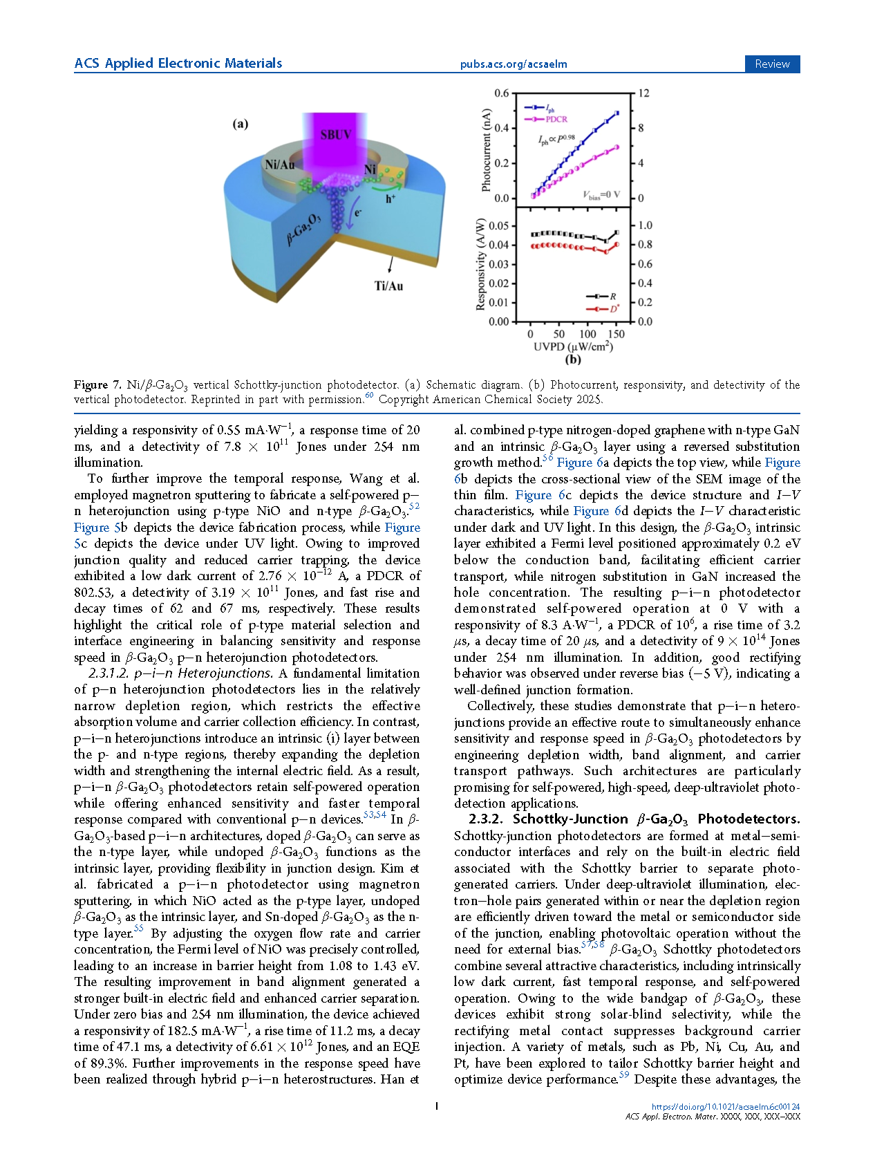
Figure 7 Ni/β−Ga₂O₃ vertical Schottky-junction photodetector. (a) Schematic diagram. (b) Photocurrent, responsivity, and detectivity of the vertical photodetector.
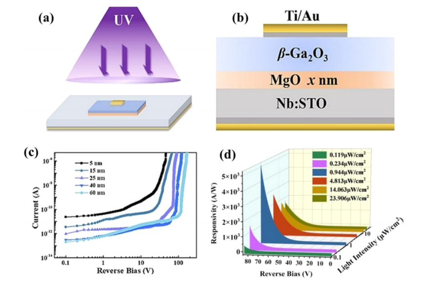
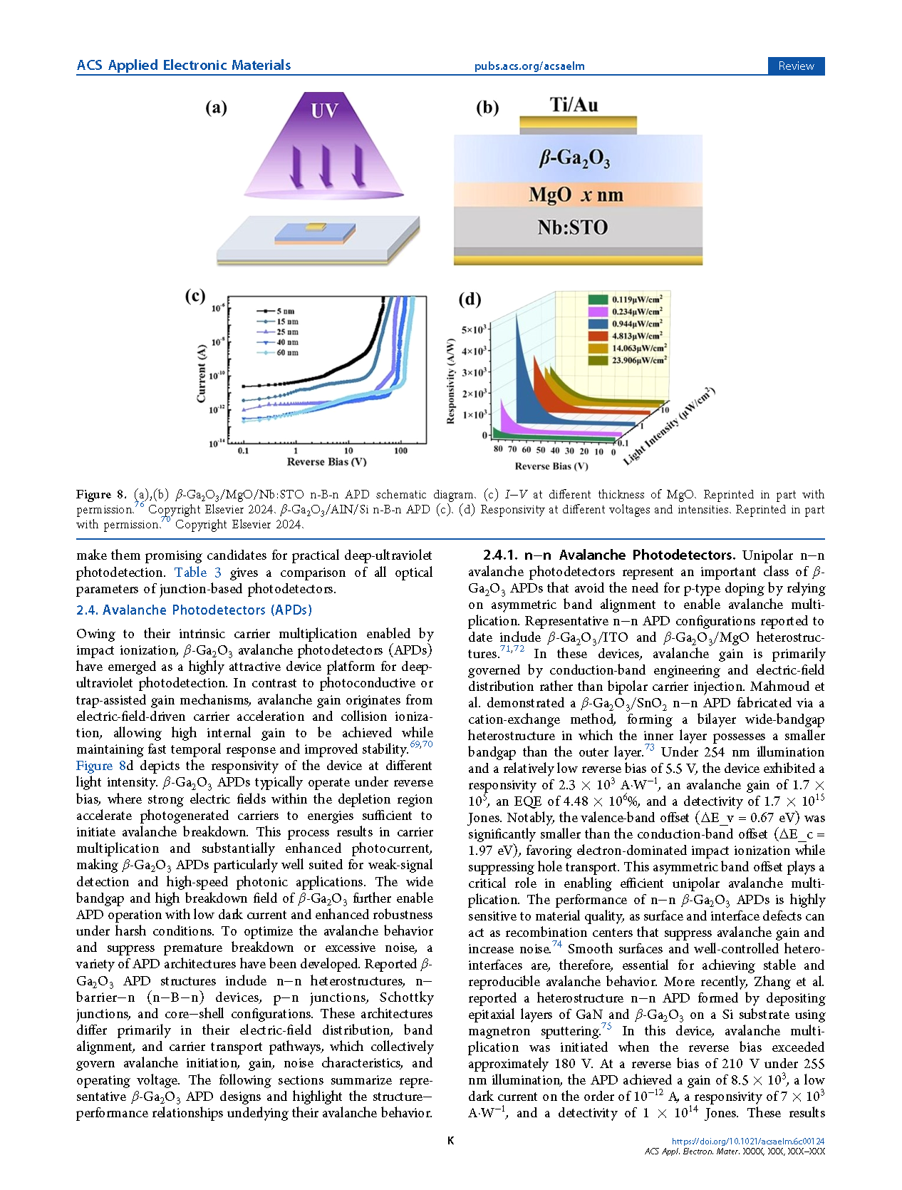
Figure 8 (a),(b) β−Ga₂O₃/MgO/Nb:STO n−B−n APD schematic diagram. (c) I−V at different thickness of MgO. β−Ga₂O₃/AlN/Si n−B−n APD. (d) Responsivity at different voltages and intensities.
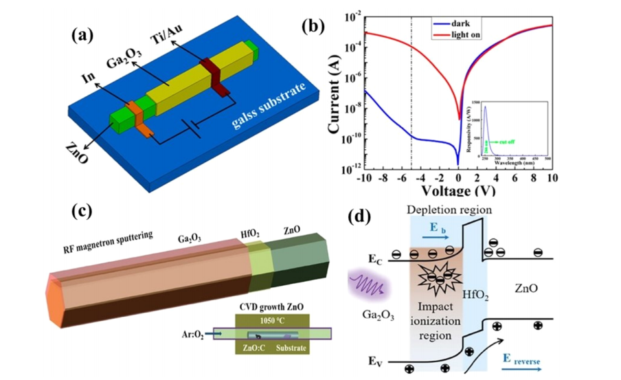
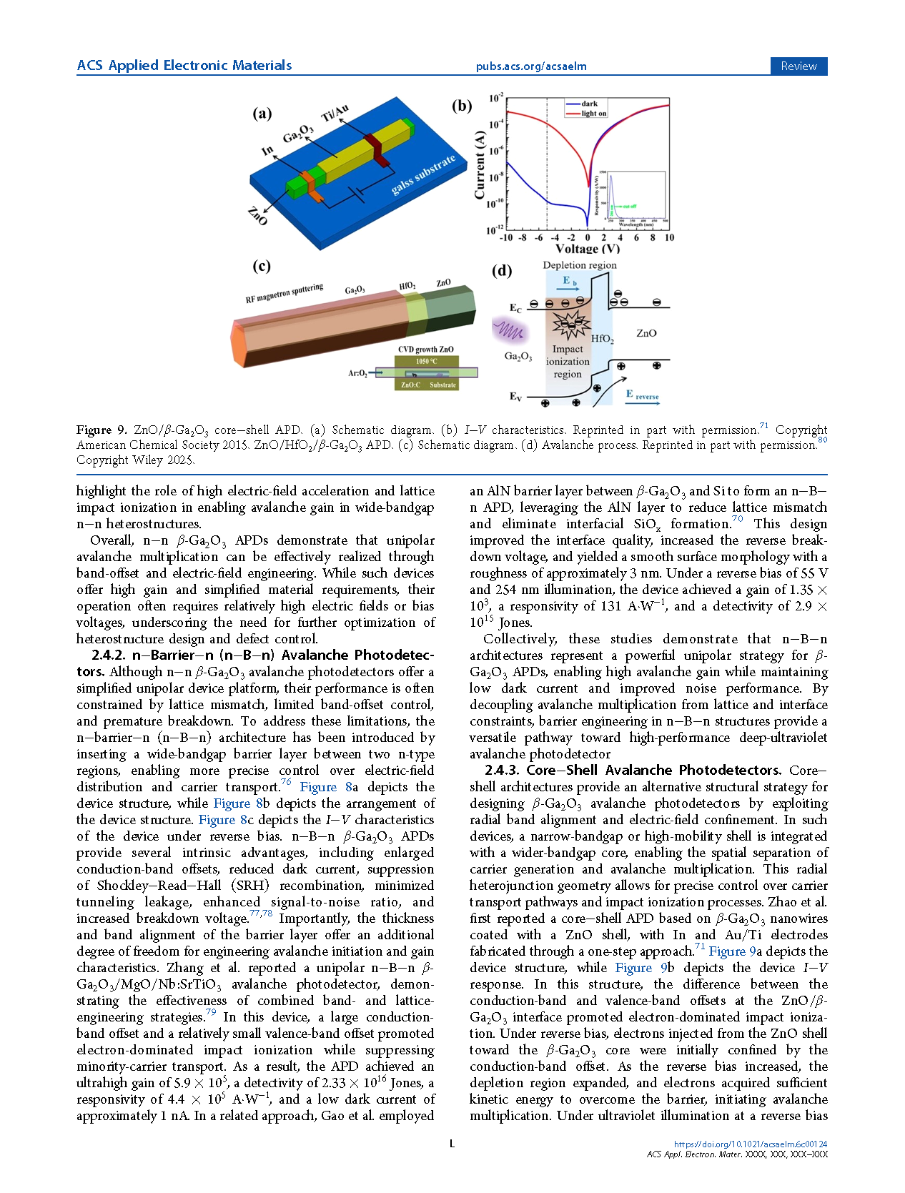
Figure 9 ZnO/β−Ga₂O₃ core−shell APD. (a) Schematic diagram. (b) I−V characteristics. ZnO/HfO₂/β−Ga₂O₃ APD. (c) Schematic diagram. (d) Avalanche process.
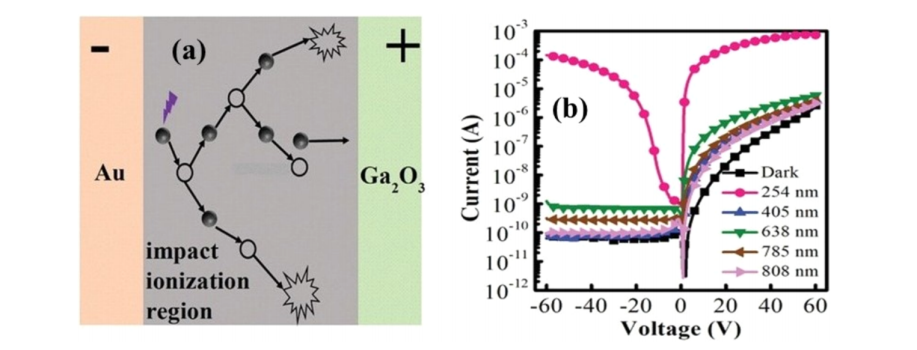
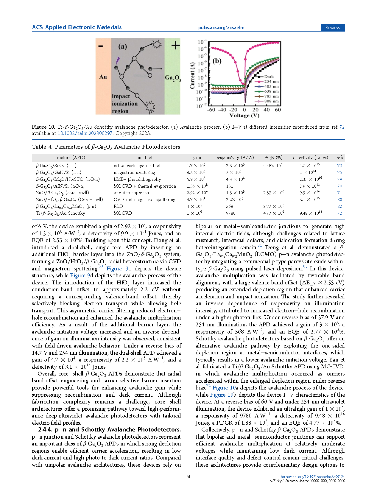
Figure 10 Ti/β−Ga₂O₃/Au Schottky avalanche photodetector. (a) Avalanche process. (b) I−V at different intensities.
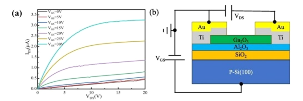
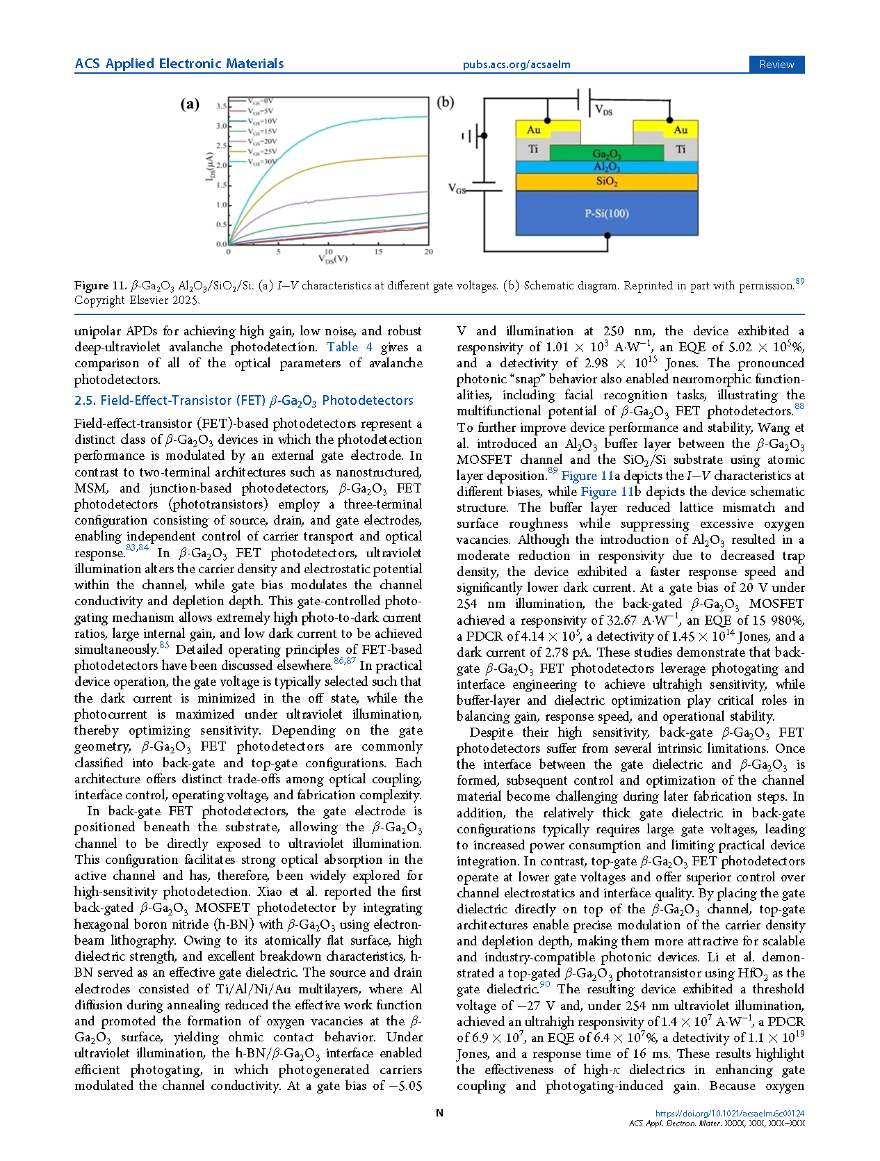
Figure 11 β−Ga₂O₃ Al₂O₃/SiO₂/Si. I−V characteristics at different gate voltages. (b) Schematic diagram.
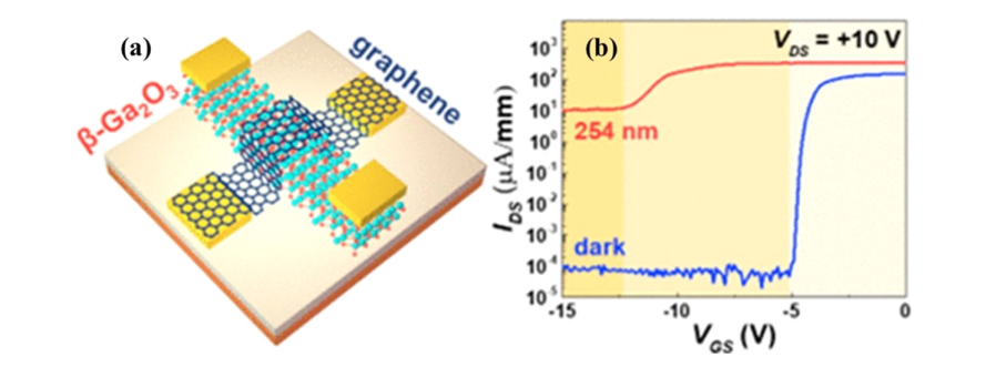
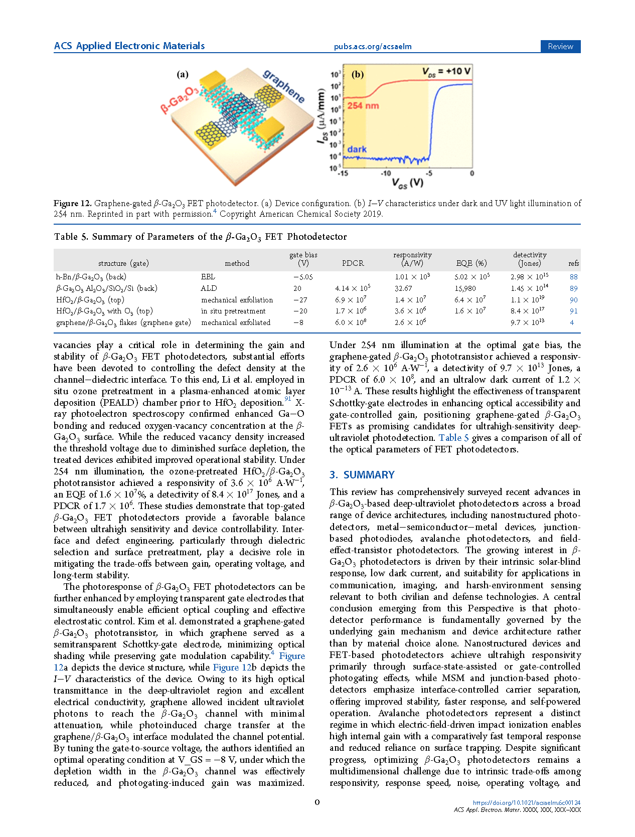
Figure 12 Graphene-gated β−Ga₂O₃ FET photodetector. (a) Device configuration. (b) I−V characteristics under dark and UV light illumination of 254 nm.
DOI:
doi.org/10.1021/acsaelm.6c00124