Paper Sharing
【Member Papers】Self-powered p/Ga₂O₃/GaN p–i–n ultraviolet photodetector with a composite material made of polypyrrole (PPy) and nitrogen-doped graphene (PGr) as the P-region
日期:2026-04-15阅读:169
Researchers from the Northeast Normal University have published a dissertation titled "Self-powered p/ Ga₂O₃/GaN p–i–n ultraviolet photodetector with a composite material made of polypyrrole (PPy) and nitrogen-doped graphene (PGr) as the P-region" in Applied Physics Reviews.
Background
Deep ultraviolet (DUV, 200–400 nm) radiation is of great significance for human life. Appropriate DUV radiation can be used for sterilization, disease treatment, and promotion of human vitamin synthesis, while excessive radiation may cause health problems. Photodetectors based on the photoelectric effect can effectively monitor DUV radiation, showing broad prospects in military and civilian applications such as special environmental detection, harmful gas sensing, space communication, and ultraviolet imaging. Traditional commercial DUV detectors (photomultiplier tubes, silicon-based diodes) have defects such as large volume, high power consumption, and reliance on filters. Wide bandgap semiconductors (AlₓGa₁₋ₓN, MgₓZn₁₋ₓO, diamond, β-Ga₂O₃) have become research hotspots, among which β-Ga₂O₃ has a suitable bandgap for the solar-blind UV band and excellent physical and chemical stability. Self-powered ultraviolet photodetectors are a research frontier, and heterojunctions exhibit better performance than Schottky junctions. However, the Ga₂O₃/GaN heterojunction suffers from interface band offset and hindered carrier transport. Introducing p-type materials to construct a p–i–n structure is an effective way to improve performance. Polypyrrole (PPy) and nitrogen-doped graphene (PGr) have excellent photoelectric properties and high mobility respectively, and their synergy can optimize device performance.
Abstract
A PPy/PGr/Ga₂O₃/GaN p–i–n heterojunction ultraviolet photodetector (UV PD) with polypyrrole (PPy) and nitrogen-doped graphene (PGr) combined as the p-region was fabricated, in which β-Ga₂O₃ was synthesized by substituting oxygen atoms for nitrogen atoms in the top layer of the GaN matrix at high temperature. In the self-powered mode, the device exhibits bimodal responses in the UVC–UVA bands. Compared with the single-peak response of the previously reported Ga₂O₃/GaN structure, the spectral response range has been greatly extended. In the UVC band, the responsivity reaches 36.4 mA/W, which is 21.4 times that of the unmodified device. The detectivity was improved to 1.5 ×10¹¹ Jones, showing an 11.3-fold enhancement. It also exhibits fast photoresponse characteristics (rise/fall times of 0.09/10.8 ms, respectively). The significant improvement of device performance is mainly attributed to the effective modification of carrier transport by PPy and PGr, which not only increases the built-in electric field at the Ga₂O₃/GaN interface but also significantly suppresses carrier recombination. The design strategy proposed in this study, based on the synergistic incorporation of organic polymers and two-dimensional materials, provides new ideas and technical references for the development of ultraviolet photodetectors with high sensitivity and broad and fast spectral response.
Highlights
A p–i–n self-powered ultraviolet photodetector with PPy/PGr composite as the p-region was constructed for the first time.
The device achieves UVC–UVA dual-band response, breaking the single-peak response limitation of traditional Ga₂O₃/GaN and greatly broadening the spectral range.
Performance is greatly improved in self-powered mode: UVC responsivity of 36.4 mA/W (21.4× enhancement), detectivity of 1.5×10¹¹ Jones (11.3× enhancement), and rise time of only 0.09 ms.
The synergistic mechanism of PPy/PGr is revealed: enhancing interface built-in electric field, optimizing band alignment, suppressing carrier recombination, and reducing device noise.
Conclusion
In summary, in this paper, Ga₂O₃/GaN heterojunctions were successfully fabricated by thermal oxidation of n-type GaN. A PPy/PGr/Ga₂O₃/GaN p–i–n ultraviolet photodetector with organic polymer and graphene combined as the P-region was constructed. Compared with the traditional Ga₂O₃/GaN device, which exhibits a single response only in the UVC band, the prepared PPy/PGr/Ga₂O₃/GaN device shows obvious dual-peak photoresponse characteristics in both the UVC and UVA bands. This enhanced photoresponse stems from the effective modification of carrier transport behavior by PPy and PGr in the device, which significantly reduces the recombination process and enhances the built-in electric field at the interface. Furthermore, PPy and PGr effectively passivate the unsaturated dangling bonds in Ga₂O₃, thereby suppressing the dark current noise of the device. The constructed p–i–n structure detector exhibits excellent self-powered performance. Without an applied bias voltage, its photoresponsivity in the UVC band reaches as high as 36.4 mA/W, which is 21.4 times that of the Ga₂O₃/GaN device without modifications. Meanwhile, the detectivity is increased to 1.5 ×10¹¹ Jones. The rise/fall response times of the device are 0.09 and 10.8 ms, respectively, indicating rapid response characteristics. This work provides an effective strategy based on the synergistic regulation of organic polymers and two-dimensional materials for the development of high-performance, multi-band response ultraviolet detectors.
Project Support
This work was supported by the National Natural Science Foundation of China (Nos. 62274027 and 62404039), the Open Research Fund of Song Shan Lake Materials Laboratory (No. 2023SLABFK03), 111 Center (B25030) and the Funding from Jilin Province (No. 20220502002GH), the Postdoctoral Fellowship Program of CPSF (No. GZC20230416), the Fundamental Research Funds for the Central Universities (No. 2412024QD010), and the Scientific Research Project of Education Department of Jilin Province (No. JJKH20250304BS).
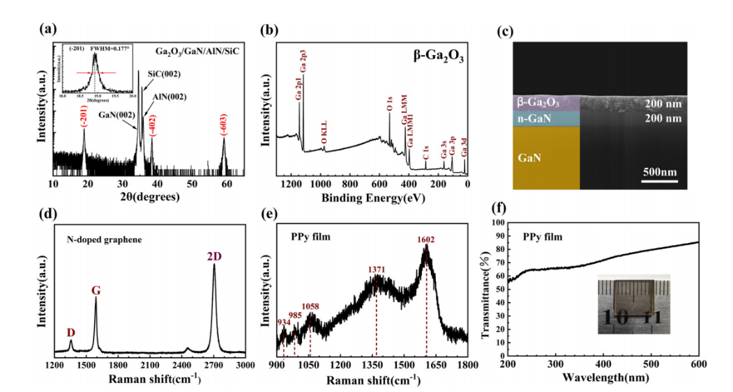
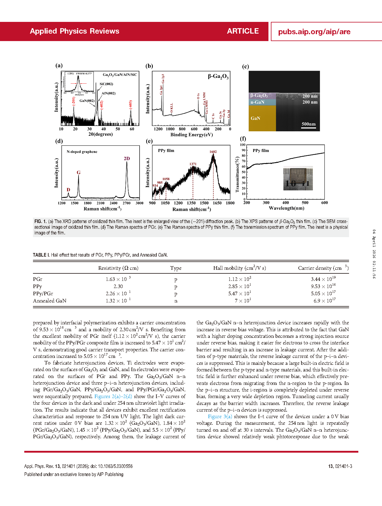
Fig. 1 (a) The XRD patterns of oxidized thin film. The inset is the enlarged view of the (201) diffraction peak. (b) The XPS patterns of β-Ga₂O₃ thin film. (c) The SEM cross-sectional image of oxidized thin film. (d) The Raman spectra of PGr. (e) The Raman spectra of PPy thin film. (f) The transmission spectrum of PPy film. The inset is a physical image of the film.
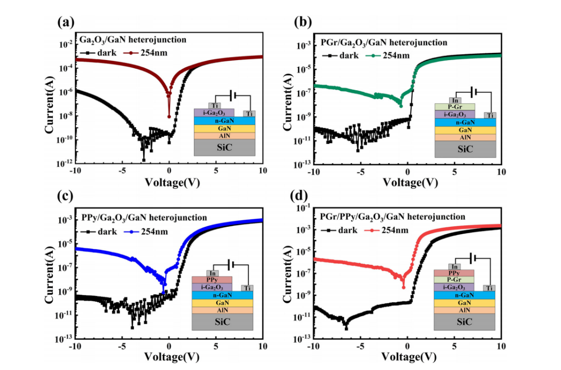
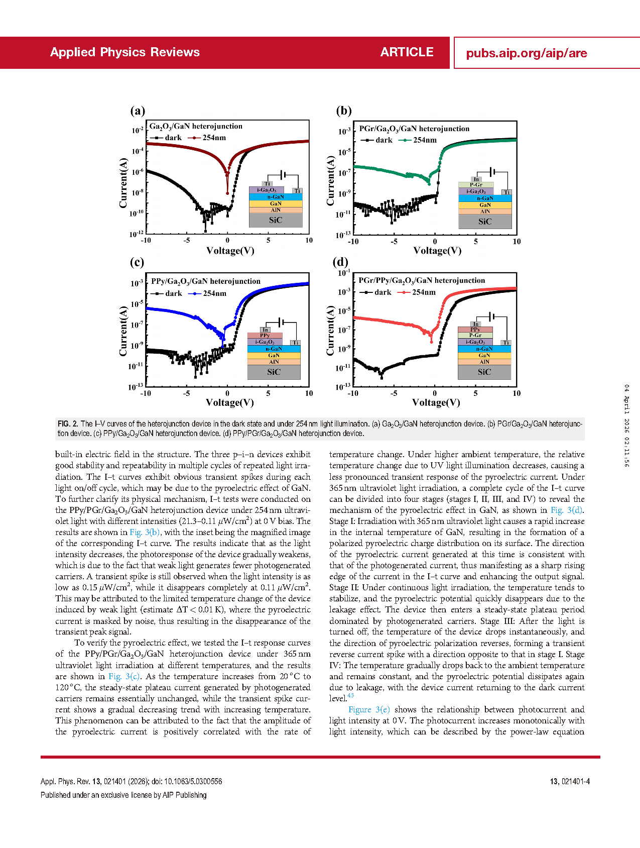
Fig. 2 The I–V curves of the heterojunction device in the dark state and under 254 nm light illumination. (a) Ga₂O₃/GaN heterojunction device. (b) PGr/Ga₂O₃/GaN heterojunction device. (c) PPy/Ga₂O₃/GaN heterojunction device. (d) PPy/PGr/Ga₂O₃/GaN heterojunction device.
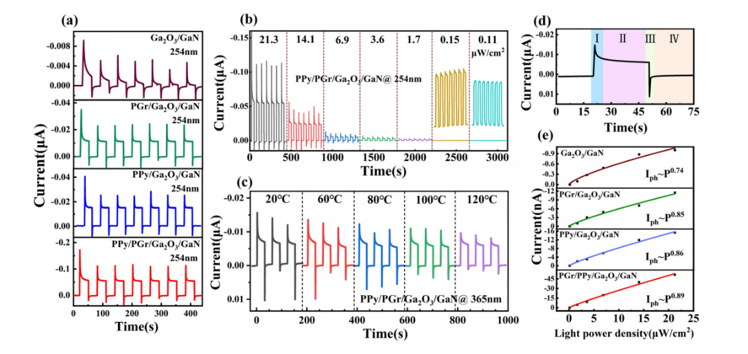
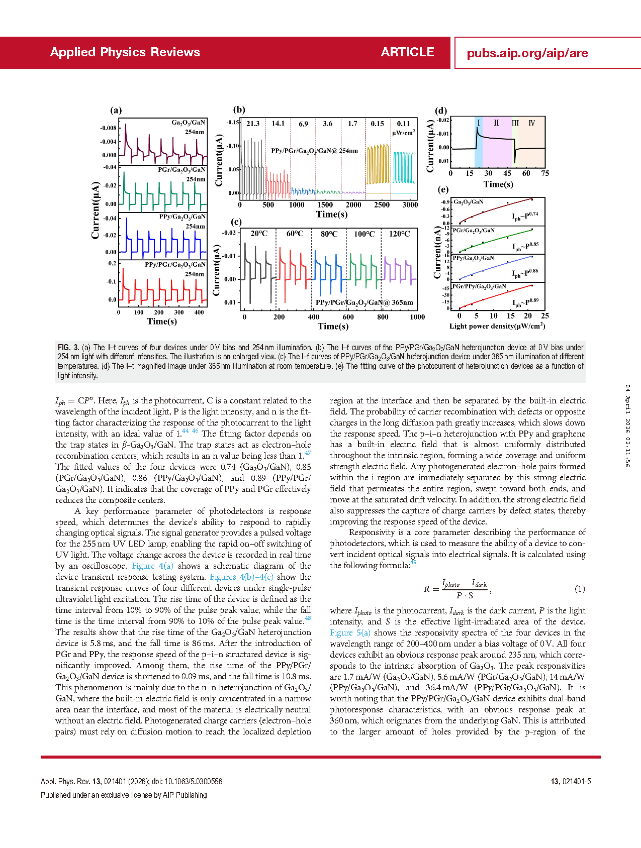
Fig. 3 (a) The I-t curves of four devices under 0 V bias and 254 nm illumination. (b) The I-t curves of the PPy/PGr/Ga₂O₃/GaN heterojunction device at 0 V bias under 254 nm light with different intensities. The illustration is an enlarged view. (c) The I-t curves of PPy/PGr/Ga₂O₃/GaN heterojunction device under 365 nm illumination at different temperatures. (d) The I–t magnified image under 365 nm illumination at room temperature. (e) The fitting curve of the photocurrent of heterojunction devices as a function of light intensity.
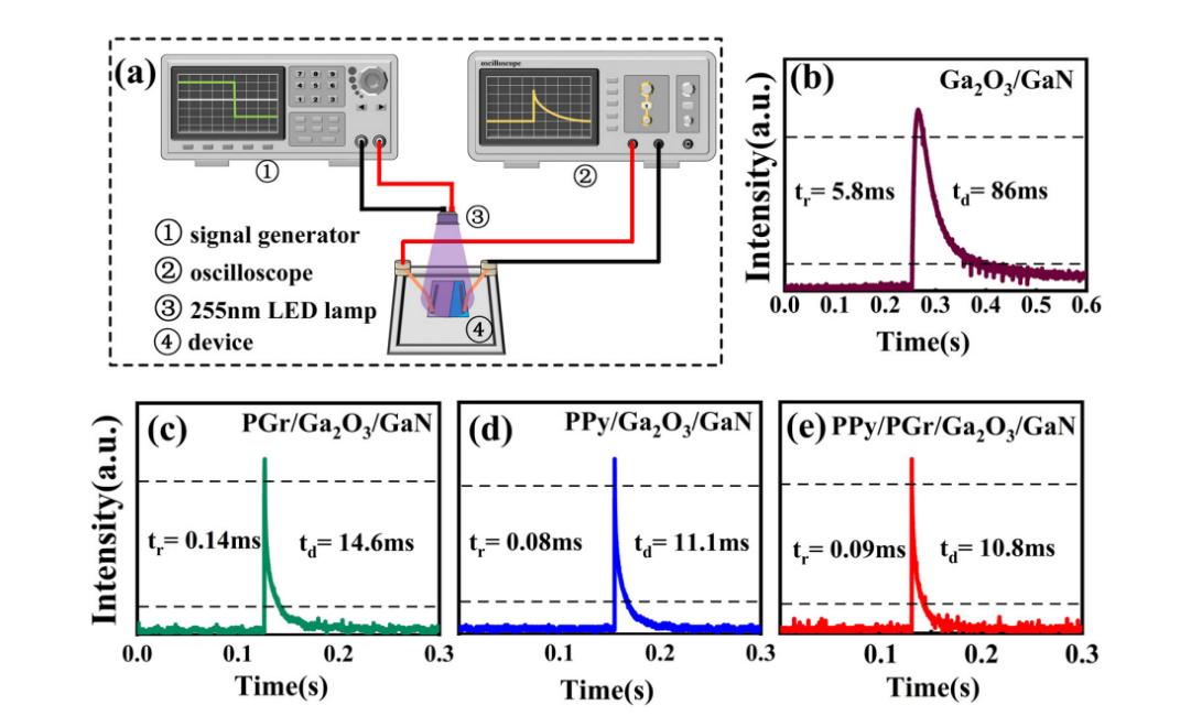
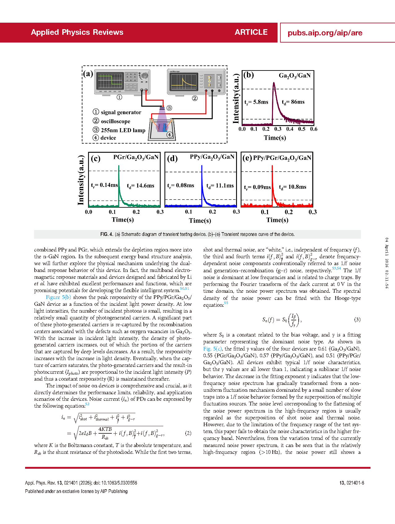
Fig. 4 (a) Schematic diagram of transient testing device. (b)–(e) Transient response curve of the device.
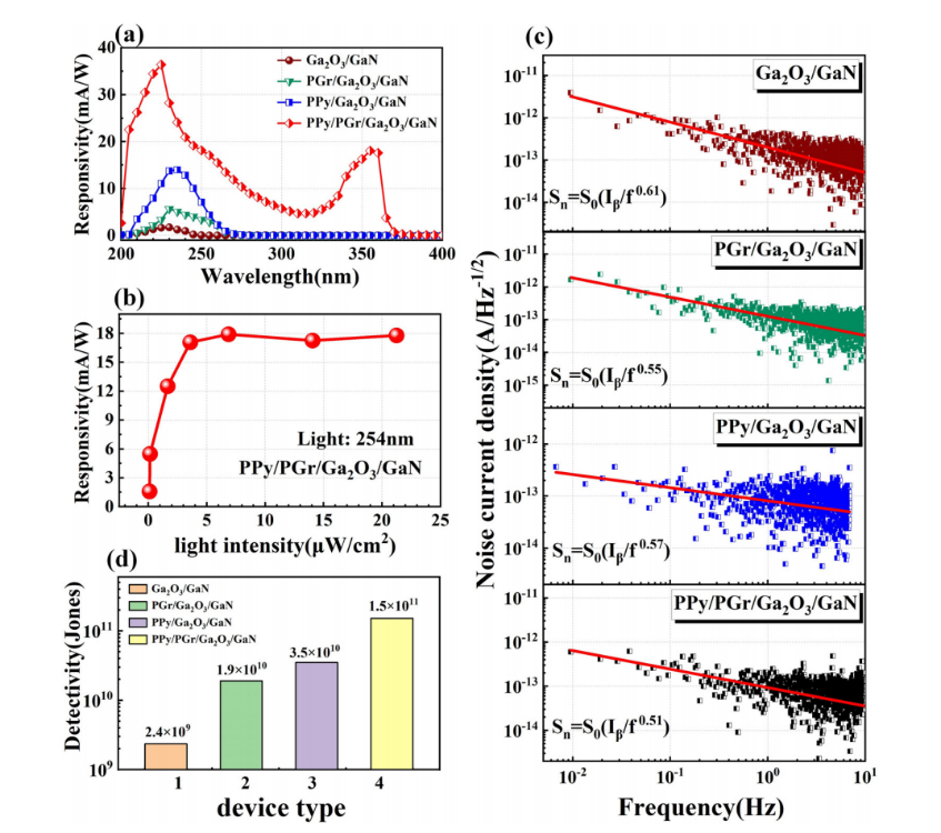
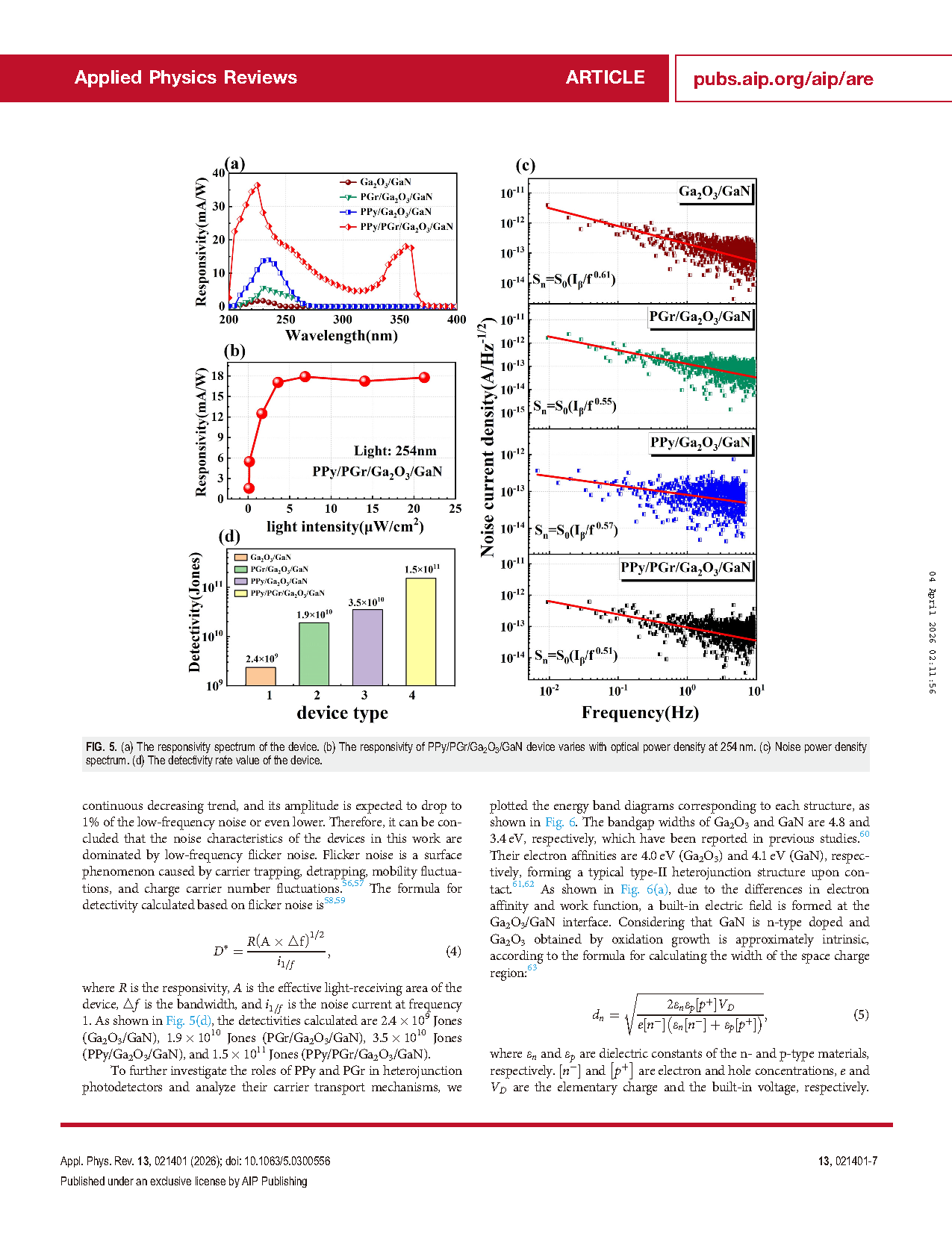
Fig. 5 (a) The responsivity spectrum of the device. (b) The responsivity of PPy/PGr/Ga₂O₃/GaN device varies with optical power density at 254 nm. (c) Noise power density spectrum. (d) The detectivity rate value of the device.
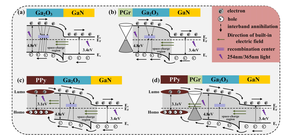
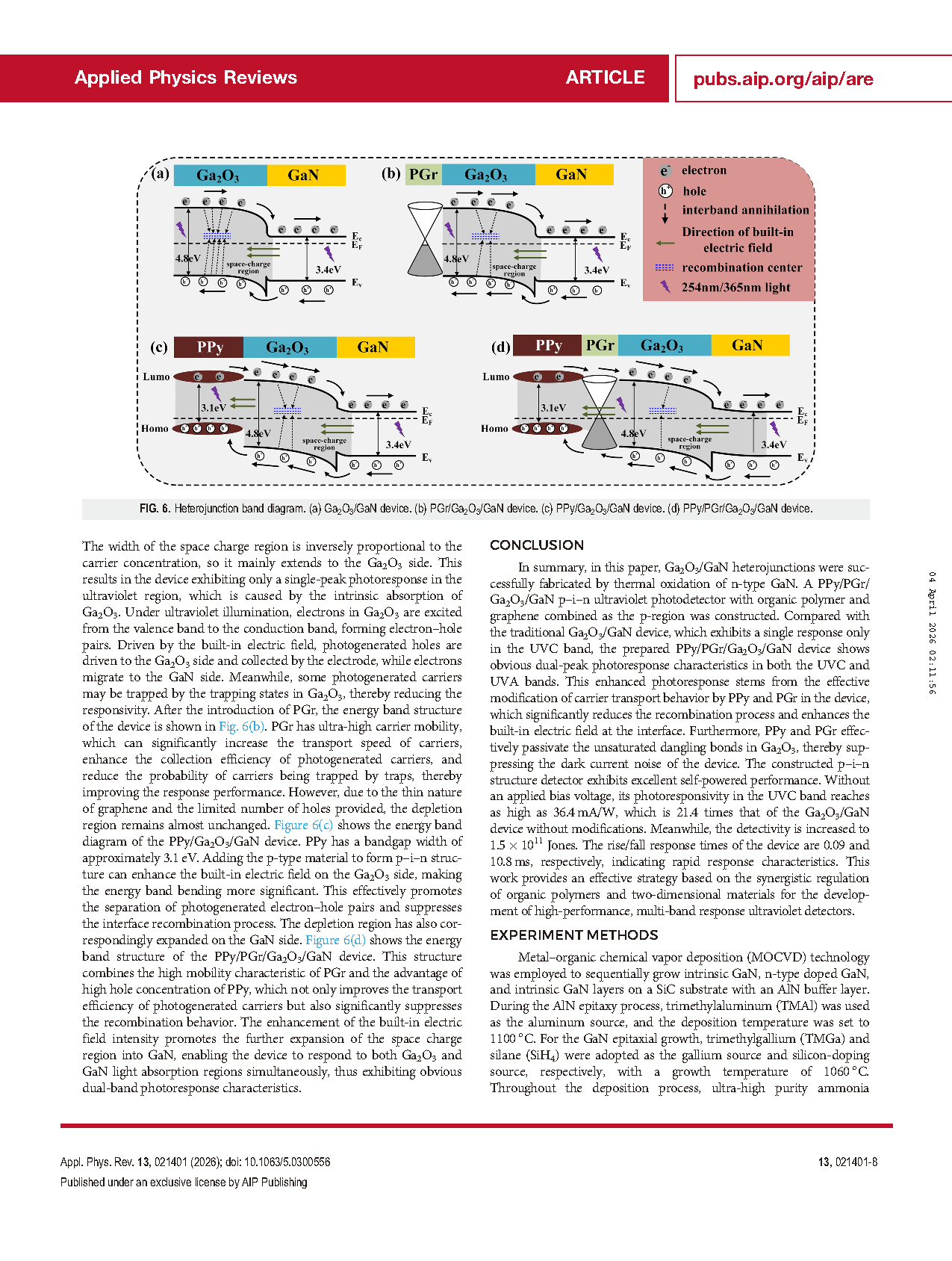
Fig. 6 Heterojunction band diagram. (a) Ga₂O₃/GaN device. (b) PGr/Ga₂O₃/GaN device. (c) PPy/Ga₂O₃/GaN device. (d) PPy/PGr/Ga₂O₃/GaN device.
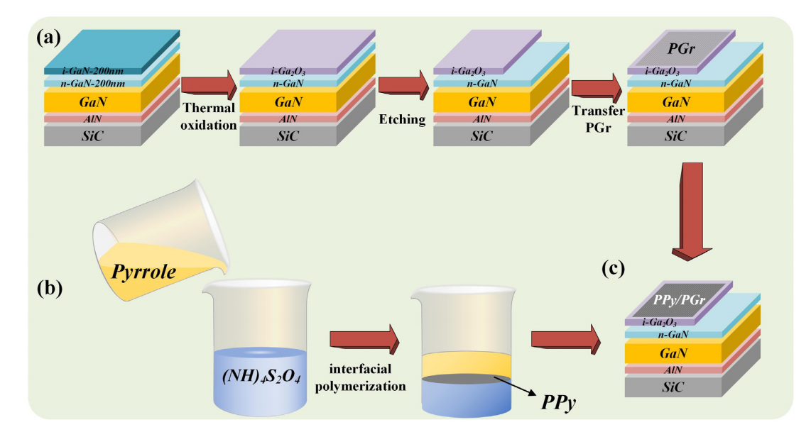
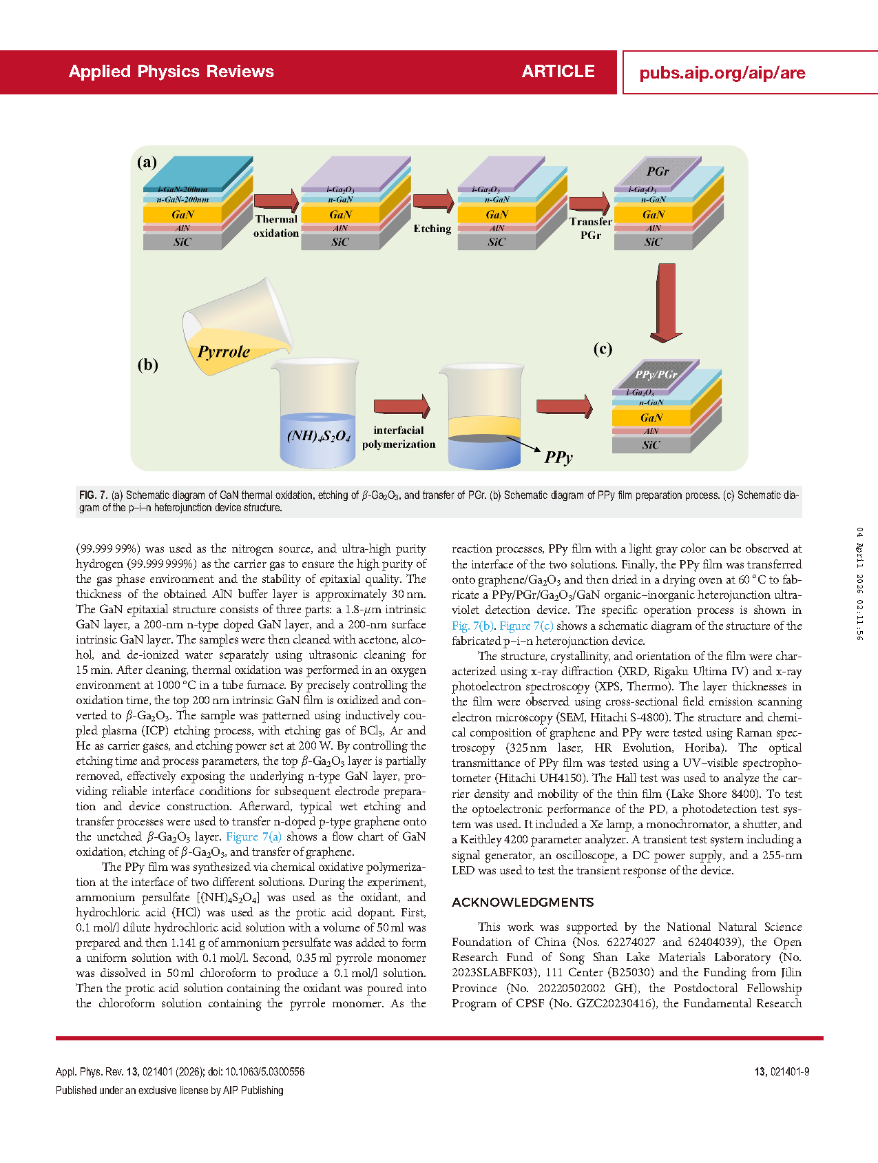
Fig. 7 (a) Schematic diagram of GaN thermal oxidation, etching of β-Ga₂O₃, and transfer of PGr. (b) Schematic diagram of PPy film preparation process. (c) Schematic diagram of the p–i–n heterojunction device structure.
DOI:
doi.org/10.1063/5.0300556