Paper Sharing
【Member Papers】Leveraging defect-induced internal gain for high-performance Ga₂O₃ photodetectors on patterned sapphire substrates
日期:2026-04-16阅读:175
Researchers from the Nanjing University of Posts and Telecommunication have published a dissertation titled "Leveraging defect-induced internal gain for high-performance Ga2O3 photodetectors on patterned sapphire substrates" in Optics Letters.
Background
β-Ga2O3, possessing a wide bandgap of 4.8 eV, is recognized as a critical material for high-power, high-temperature, and deep-ultraviolet (DUV) photodetectors (PD), attributed to its outstanding thermal stability and elevated breakdown field. In contrast to AlGaN, which necessitates compositional adjustments for DUV detection, β-Ga2O3 efficiently detects DUV without external filters, streamlining device design. Furthermore, β-Ga2O3 can be produced through multiple scalable methods, including Chemical Vapor Deposition (CVD), Molecular Beam Epitaxy (MBE), and melt growth, offering a cost-efficient pathway for large-area substrate fabrication. Patterned sapphire substrates (PSS) are widely utilized to elevate the quality of heteroepitaxial films, reducing dislocation densities and optimizing the optoelectronic performance of devices. Despite substantial research on α-Ga2O3 grown on PSS, investigations of β-Ga2O3 have been limited. Recent studies demonstrate that the predicted enhancement in film quality and PD performance via epitaxial lateral overgrowth (ELO) on PSS has not been achieved for β-Ga2O3 by Metal-Organic Chemical Vapor Deposition (MOCVD), highlighting the need for further investigation into growth techniques and optimization for β-Ga2O3-based optoelectronic devices.
Abstract
We report a deep-ultraviolet (DUV) metal–semiconductor-metal (MSM) photodetector based on a β-Ga2O3 thin film deposited by chemical vapor deposition (CVD) on a patterned sapphire substrate (PSS), compared with a control device using a film grown on flat sapphire. To the best of our knowledge, this is the first demonstration of β-Ga2O3 films with a preferred (510) orientation. The film grown on PSS exhibited high defect densities, including structural disorders, oxygen vacancies, and dangling bonds, which enabled exceptional responsivity 106.5 A/W and specific detectivity 1.36 ×10¹³ Jones through strong internal gain and extrinsic transitions, despite a relatively large dark current. A UV/visible rejection ratio R255/R400 above 104 further confirmed the device’s sensitivity. A comprehensive analysis was performed on the impact of defects on the increased dark current and slower response. These findings offer important insights into the growth mechanism of β-Ga2O3 on PSS and highlight its potential for scalable, cost-effective solar-blind photodetectors.
Highlights
• A β-Ga2O3 thin film with a preferential (510) orientation, the first of its kind, was successfully grown on a patterned sapphire substrate (PSS) via chemical vapor deposition (CVD), providing a brand-new direction for the crystallographic orientation control and growth mechanism research of β-Ga2O3.
• A simple unmodified CVD system was adopted to fabricate PSS-basedβ-Ga2O3 thin films and fabricate metal-semiconductor-metal (MSM) photodetectors thereupon. Featuring a simple process, cost controllability and easy scalability, this method breaks through the technical limitations in the fabrication of existing PSS-based β-Ga2O3 devices.
• High-performance detection of β-Ga2O3devices was achieved for the first time by leveraging defect-induced internal gain, which transforms defects from a performance-impairing factor into a driving force for performance enhancement and offers a novel approach for the performance regulation of β-Ga₂O₃ devices.
• Combined with the optoelectronic performance tests of the devices, comprehensive characterizations including X-ray diffraction (XRD), X-ray photoelectron spectroscopy (XPS) and photoluminescence (PL) were conducted to fully reveal the dual-effect regulation mechanism of defects on β-Ga2O3 photodetectors, thus providing critical theoretical and experimental foundations for the precise defect control and performance optimization of β-Ga2O3 devices.
Conclusion
In conclusion, a DUV PD based on β-Ga2O3 grown on PSS has been successfully fabricated by CVD, and its optoelectronic performance has been presented and discussed in detail. The as-grown β-Ga2O3 thin film possessed multiple defects, due to its low crystallinity, rough surface, and rough incomplete ELO. These defects contributed to a high internal gain and PPC effect on the PD, resulting in higher current outputs while decreasing response time. The PD exhibits a R of 106.5 A/W, an EQE of 5.18×10⁴ ,a D* of 1.36×10¹³ , and an UV/visible light rejection ratio over 104 , suggesting a high-performance DUV photodetection based on the cost-effective and easy-to-operate CVD system. This high performance, combined with the ease of largescale and cost-effective fabrication, suggests that the findings of this study demonstrate a promising approach and highlight the potential for developing high-performance solar-blind photodetectors based on PSS/CVD β-Ga2O3. However, achieving cost-effective mass production will require significant future efforts to overcome key challenges such as ensuring large-area film thickness uniformity, controlling defect formation consistently across full-size wafers, and scaling up the PSS growth process to achieve high yield. Future work will focus on addressing these scalability challenges to realize the pathway towards commercial applications.
Project Support
National Natural Science Foundation of China (62374094, 62474095); Natural Science Foundation of Nanjing University of Posts and Telecommunications (NY224131, NY224084).
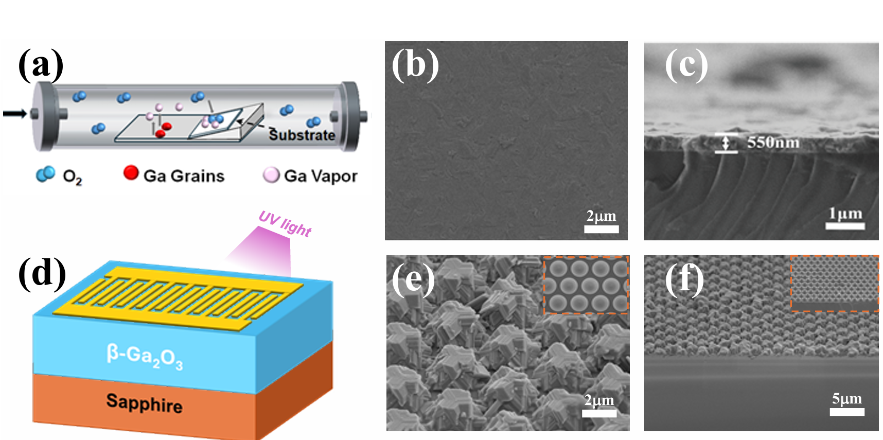
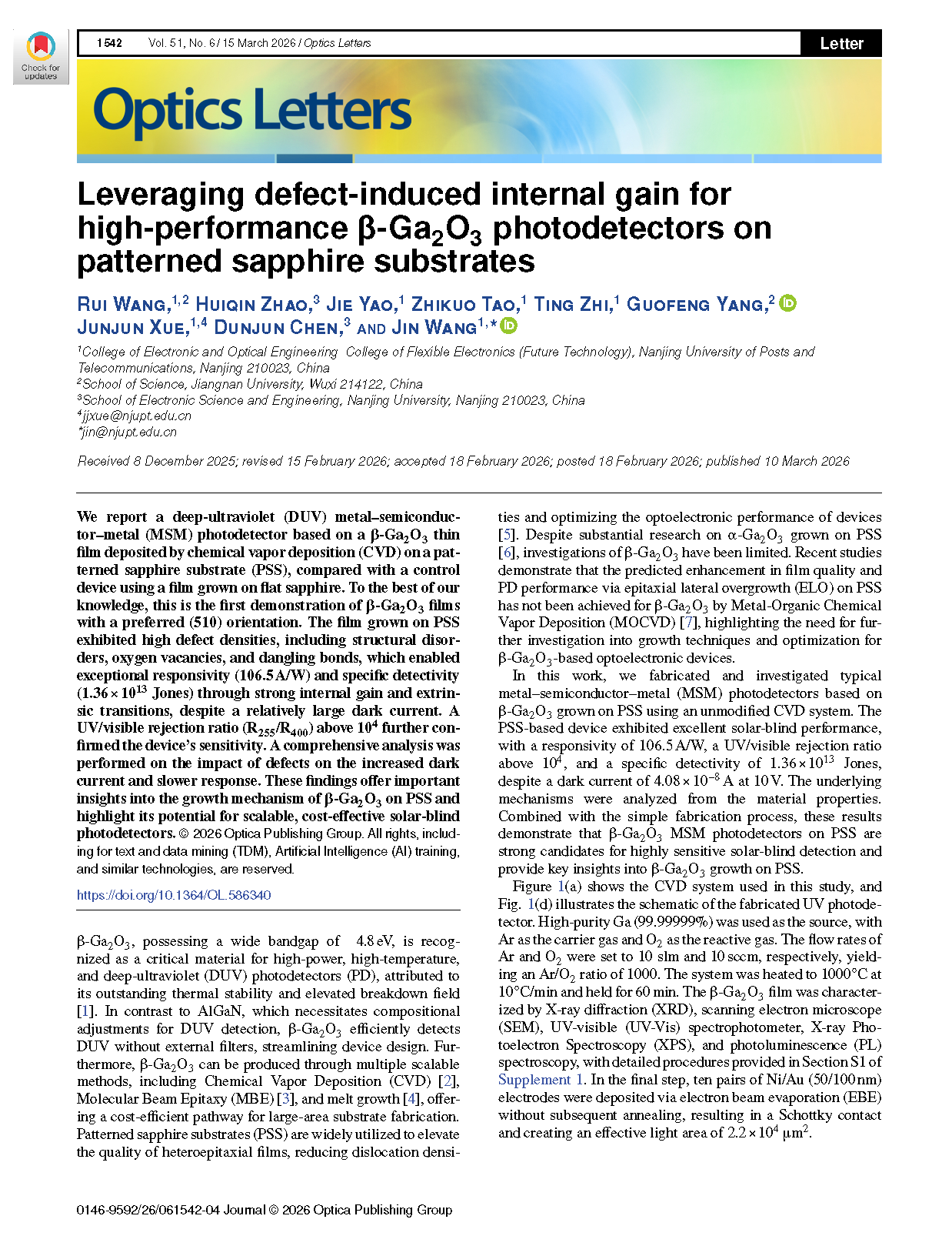
Fig. 1. (a) The CVD system and the deposition process of β-Ga2O3 films. Top-view SEM images of the β-Ga2O3 film deposited on (b) sapphire, and (e) PSS. (d) Schematic diagram of the prepared β-Ga2O3 UV PD. Cross-sectional SEM images of β-Ga2O3 film deposited on (c) sapphire, and (f) PSS. The orange dashed section shows the SEM image of the original PSS.
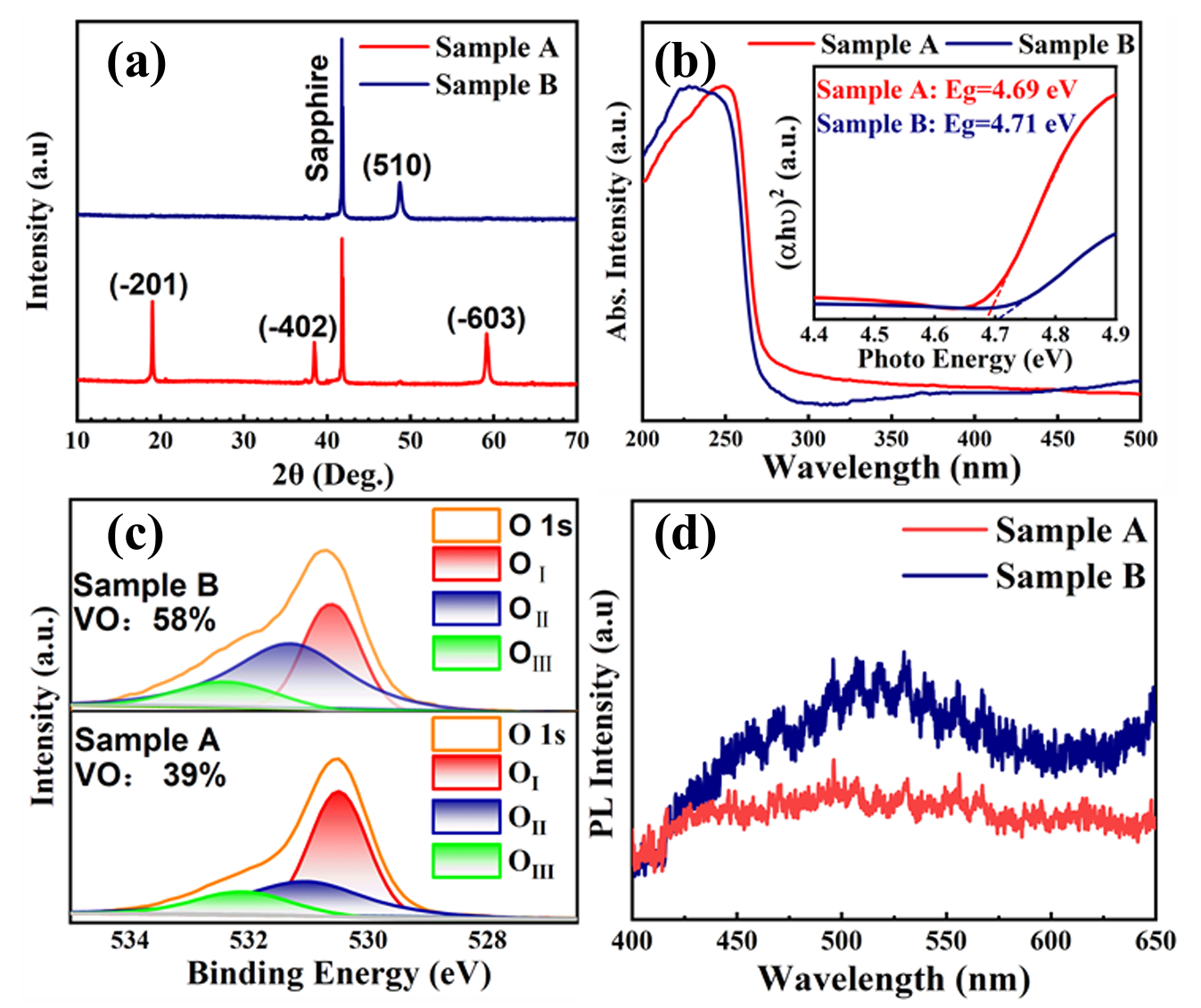
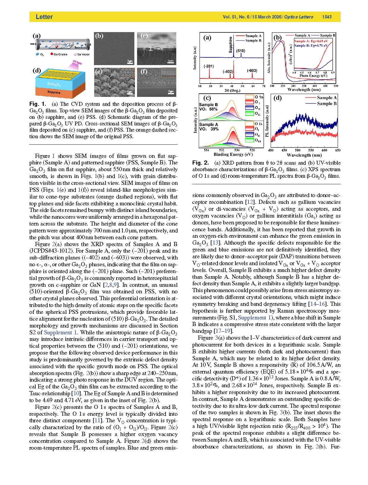
Fig. 2. (a) XRD pattern from θ to 2θ scans and (b) UV-visible absorbance characterizations of β-Ga2O3 films. (c) XPS spectrum of O 1 s and (d) room-temperature PL spectra from β-Ga2O3 films.
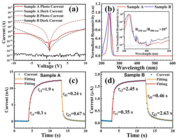
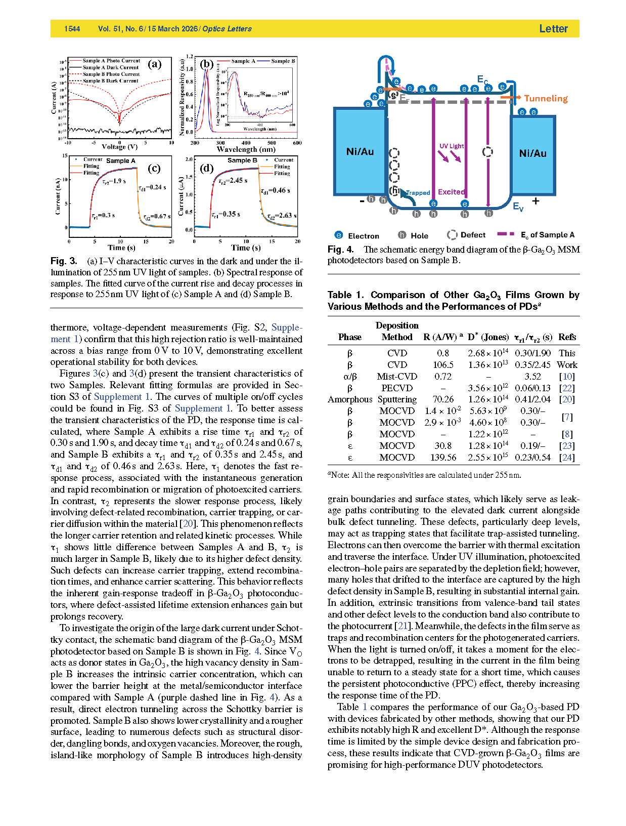
Fig. 3. (a) I–V characteristic curves in the dark and under the illumination of 255 nm UV light of samples. (b) Spectral response of samples. The fitted curve of the current rise and decay processes in response to 255 nm UV light of (c) Sample A and (d) Sample B.
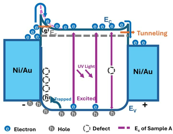
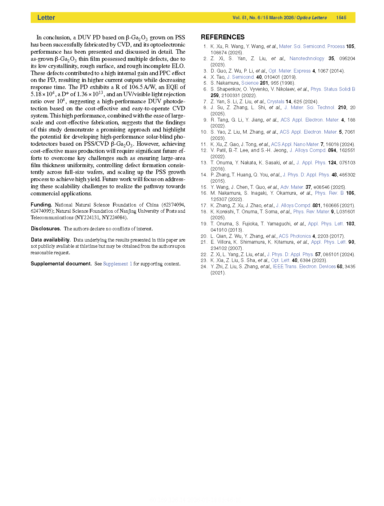
Fig. 4. The schematic energy band diagram of the β-Ga2O3 MSM photodetectors based on Sample B.
DOI:
doi: 10.1364/OL.586340.