Paper Sharing
【Member Papers】Aluminum Nanoparticle-Enhanced a-Ga₂O₃ Solar-Blind UV Photodetectors with High-Performance via Localized Surface Plasmon Resonance
日期:2026-04-16阅读:204
A research team from Xi’an University of Posts and Telecommunications has published a paper in the IEEE Sensors Journal titled “Aluminum Nanoparticle-Enhanced a-Ga₂O₃ Solar-Blind UV Photodetectors with High Performance via Localized Surface Plasmon Resonance.” The study proposes a simple performance-optimization strategy based on localized surface plasmon resonance (LSPR) induced by aluminum nanoparticles (Al-NPs) to address the inherently low responsivity of amorphous gallium oxide (a-Ga₂O₃) solar-blind ultraviolet photodetectors, achieving significant device performance enhancement.
Background
The solar-blind ultraviolet (UV) band (200–280 nm) is strongly absorbed by the ozone layer in the Earth’s atmosphere, forming a low-background-noise detection window at the surface. This makes solar-blind UV photodetectors highly valuable for applications such as optical communications, missile warning systems, corona discharge detection, fire alarm systems, and space exploration.
Gallium oxide (Ga₂O₃), as an emerging ultra-wide bandgap semiconductor (bandgap: 4.4–5.3 eV), naturally matches the solar-blind UV spectrum without requiring complex alloy engineering. It also offers excellent thermal stability, radiation resistance, high-voltage tolerance, and chemical stability. Compared with crystalline Ga₂O₃, which requires high-temperature growth and lattice-matched substrates, amorphous Ga₂O₃ can be deposited at low temperatures, features simple processing, large-area uniformity, low manufacturing cost, and better compatibility with flexible substrates. It has therefore become a research hotspot in UV photodetectors.
However, a key limitation of metal–semiconductor–metal (MSM) photodetectors is that the metal electrodes partially block incident light, restricting optical absorption and responsivity enhancement. Therefore, improving optoelectronic performance under the constraints of low cost and simple processing remains an important challenge.
Importantly, unlike visible and infrared photodetectors, UV light has an extremely short absorption depth; photons are almost fully absorbed within the active layer. As a result, traditional light-trapping or backside reflector strategies are largely ineffective. Improving UV responsivity therefore relies not on increasing photon capture, but on enhancing the absorption-to-conversion efficiency through improved optoelectronic coupling.
Main Content
To address the limited responsivity of a-Ga₂O₃ solar-blind UV photodetectors, the researchers deposited a ~135 nm a-Ga₂O₃ thin film on the substrate using atomic layer deposition (ALD) and fabricated an MSM UV photodetector.
Subsequently, phosphoric acid wet etching was used to optimize the film surface, followed by deposition of an ultrathin Al layer and thermal annealing. This process successfully formed aluminum nanoparticles (Al-NPs) with a diameter of approximately 60–70 nm on the device surface, resulting in an Al-NPs/a-Ga₂O₃ hybrid photodetector structure.
Key Innovations
Proposed a performance-enhancement strategy for a-Ga₂O₃ solar-blind UV photodetectors based on Al nanoparticle surface modification.
Achieved simultaneous surface morphology optimization and localized surface plasmon resonance enhancement via phosphoric acid etching combined with Al-NP formation.
Demonstrated that scattering coupling and LSPR effects from Al nanoparticles significantly enhance optical absorption and carrier excitation, thereby improving device photoresponse.
The method features simple processing, low cost, and good reproducibility, providing a practical pathway for improving a-Ga₂O₃ optoelectronic devices.
A key insight of this work is that, compared with conventional SPR hot-carrier enhancement studies, the performance may not represent the absolute state-of-the-art, but it demonstrates an extremely simple and broadly accessible fabrication strategy: ultrathin metal film deposition followed by annealing-induced self-aggregation into nanoparticles. This is a universally applicable approach that most laboratories can easily implement.
Figures
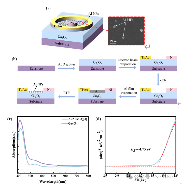
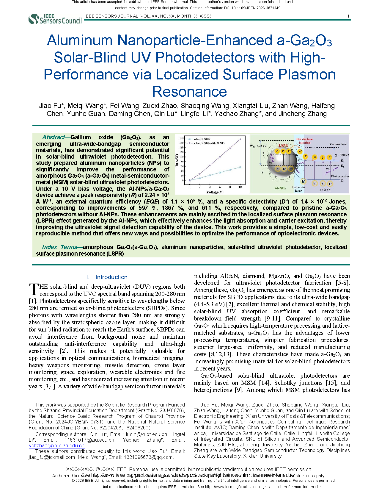
Figure 1 shows the process flow. This self-assembly approach avoids complex micro/nanofabrication steps, offering high experimental accessibility and universality, and enabling a practical route toward low-cost, scalable SPR-enhanced devices.(a) Device structure schematic and SEM images of Al-NPs/a-Ga₂O₃ composite film (b) Fabrication process flow (c) UV–visible absorption spectra of a-Ga₂O₃ and Al-NPs/a-Ga₂O₃ films (d) (αhν)²–hν plot of a-Ga₂O₃ film
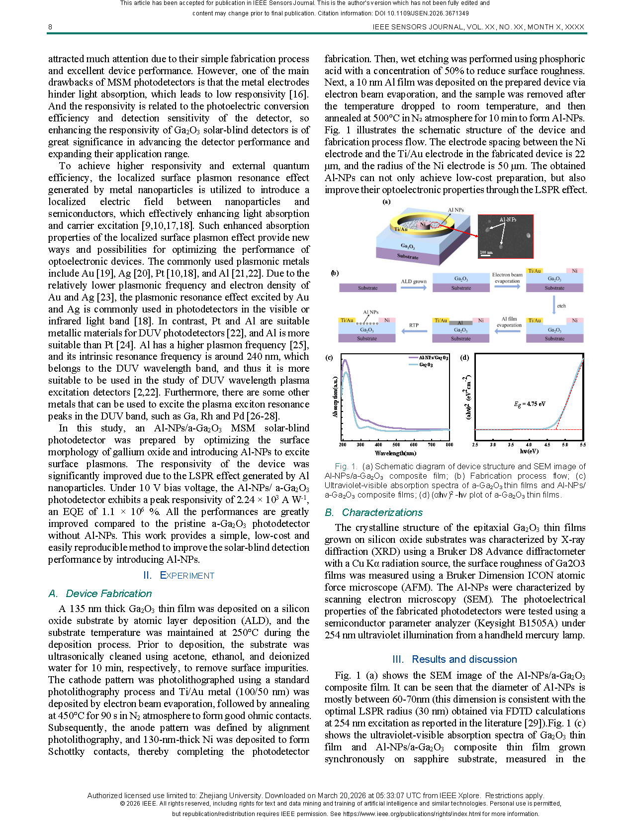
AFM results show that phosphoric acid etching significantly reduces surface roughness, facilitating uniform Al-NP distribution and plasmonic enhancement. After Al-NP introduction, the composite film exhibits significantly enhanced deep-UV absorption (200–260 nm), indicating improved utilization of solar-blind UV photons.
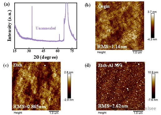
Figure 2 (a) XRD pattern of Ga₂O₃ film (b) AFM image of Ga₂O₃ film (c) AFM image after phosphoric acid etching (d) AFM image after etching, Al deposition, and rapid thermal annealing
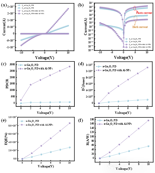
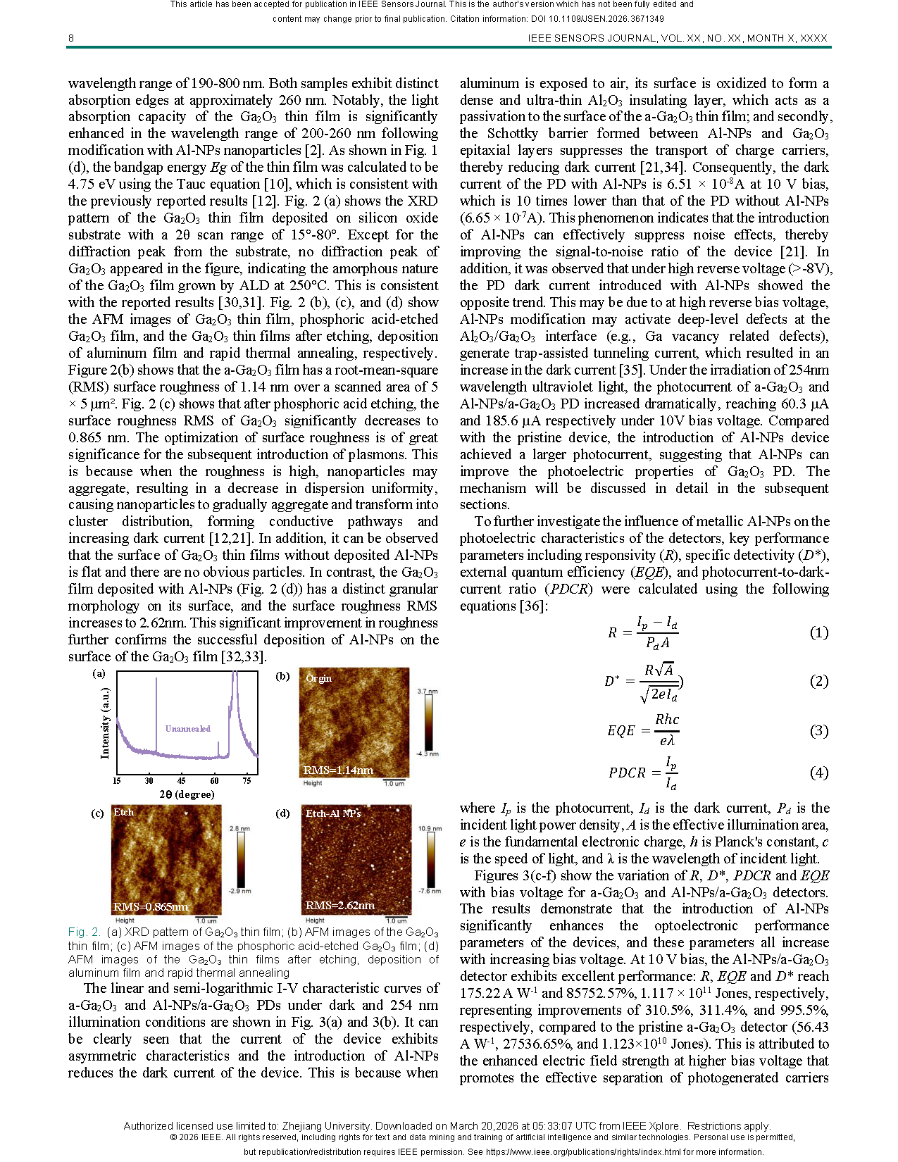
Figure 3 I–V curves of devices with and without Al-NPs (linear scale) (b) logarithmic scale (c) PDCR (d) D* (e) EQE (f) Responsivity (R) as a function of bias voltage
Device measurements under 254 nm illumination show that Al-NP-modified detectors significantly outperform unmodified ones. At 10 V bias, the dark current decreases from 6.65 × 10⁻⁷ A to 6.51 × 10⁻⁸ A, while the photocurrent increases from 60.3 μA to 185.6 μA, indicating suppressed leakage current and enhanced carrier generation and collection.
Further measurements show that at 0.5 mW/cm² and 10 V bias, the optimized device achieves:
Responsivity: 2242.5 A/W
External quantum efficiency: 1.1 × 10⁶%
Specific detectivity: 1.4 × 10¹² Jones
Compared with the unmodified device, these represent improvements of 597.0%, 611.1%, and 1866.7%, respectively, demonstrating excellent overall photodetection performance.
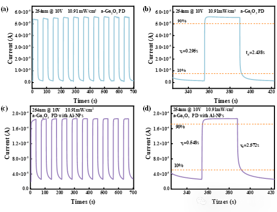
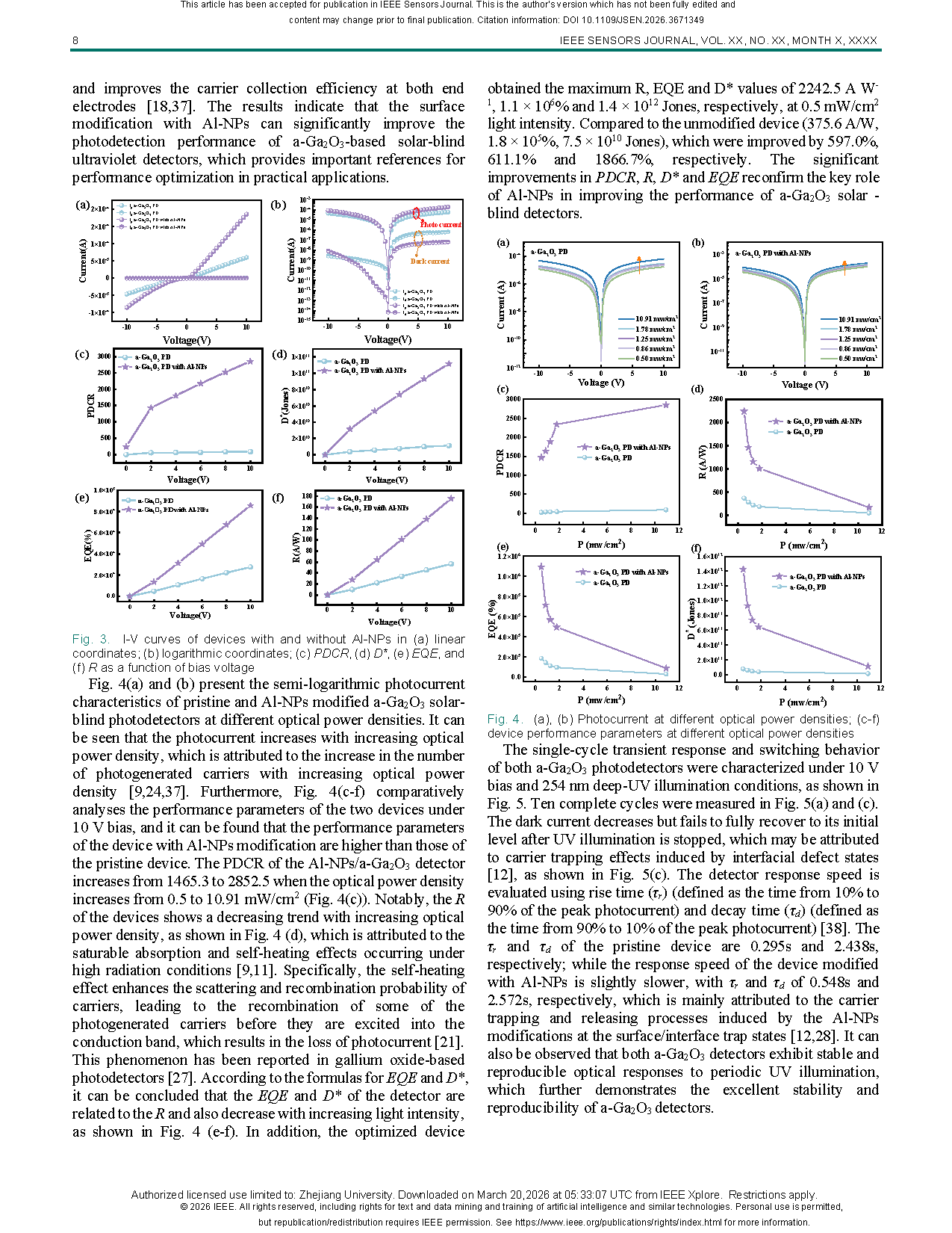
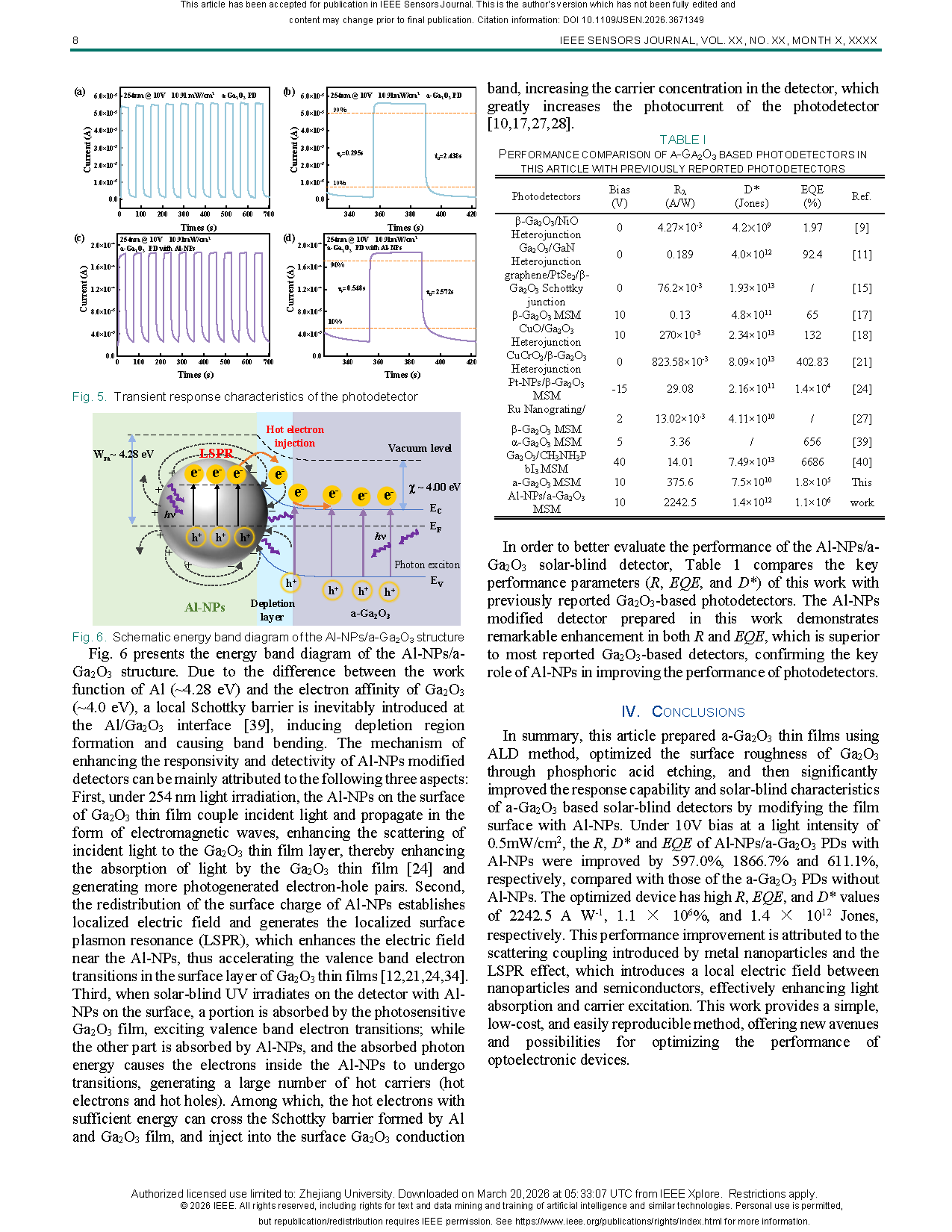
Figure 4 shows transient photoresponse characteristics.
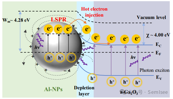
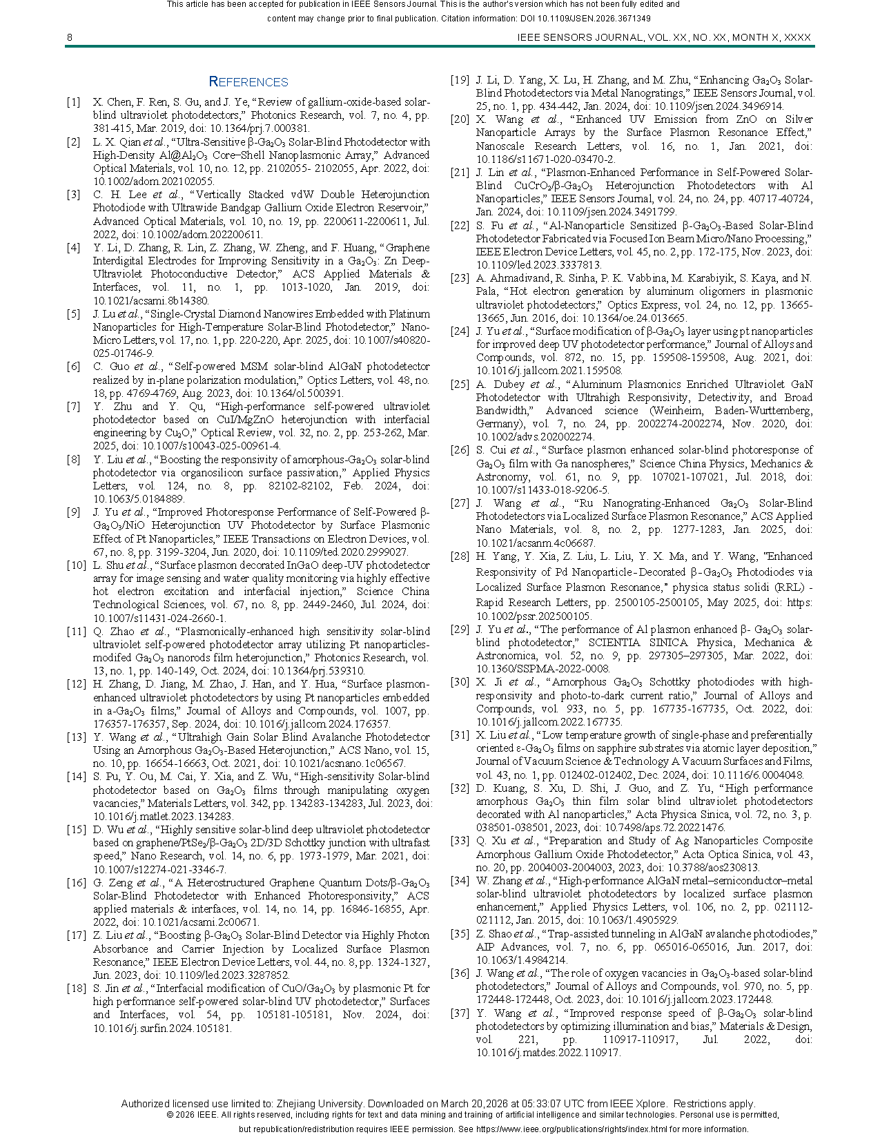
Figure 5 illustrates the SPR hot-carrier mechanism.
Mechanism Interpretation:The performance enhancement is attributed to scattering coupling and localized surface plasmon resonance induced by metallic nanoparticles. The nanoparticles generate a localized electromagnetic field at the metal–semiconductor interface, effectively enhancing optical absorption and carrier excitation.
Funding
This work was supported by the Education Department of Shaanxi Province (Grant No. 23JK0676), the Natural Science Foundation of Shaanxi Province (2024JC-YBQN-0731), and the National Natural Science Foundation of China (62204203, 62406260).