


Member News
【Member News】Fujia Gallium Showcases at the 2026 Semiconductor New Materials Development (Deyang) Conference; Chairman Qi Hongji Invited to Discuss Key Issues in Gallium Oxide Industrialization
日期:2026-04-20阅读:274
Hangzhou Fujia Gallium Technology Co., Ltd. presented its latest exhibits at the 2026 Semiconductor New Materials Development (Deyang) Conference. Chairman and Researcher Qi Hongji was invited to deliver a keynote report titled “Perspectives on the Industrialization of Fourth-Generation Semiconductor Gallium Oxide.”
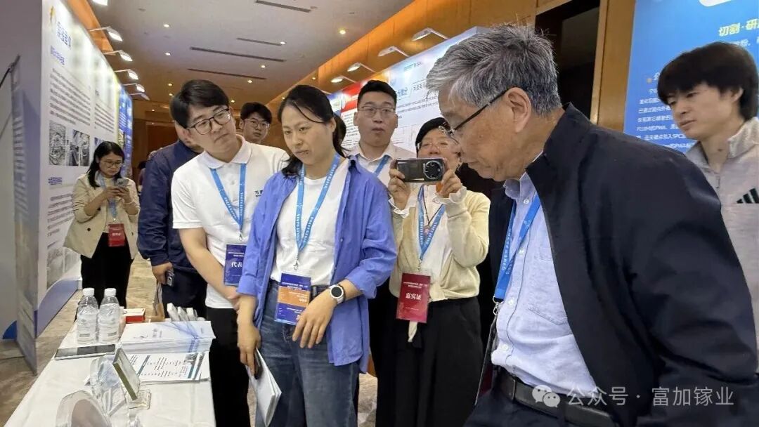
From April 15 to 18, the conference—hosted by the Semiconductor Materials Branch of the China Electronic Materials Industry Association—was grandly held in Deyang, Sichuan Province. Centered on the theme “Leading Wide Bandgap, Building a New Ecosystem,” the event brought together top experts, leading enterprises across the industrial chain, and key innovation forces nationwide. Hangzhou Fujia Gallium Technology Co., Ltd. (hereinafter referred to as “Fujia Gallium”) participated with its exhibits, while Chairman Qi Hongji shared insights on the industrialization pathway of Gallium Oxide, engaging with industry peers to explore future development directions.
Full Industry Chain Showcase Highlights Fujia Gallium’s Leading Capabilities
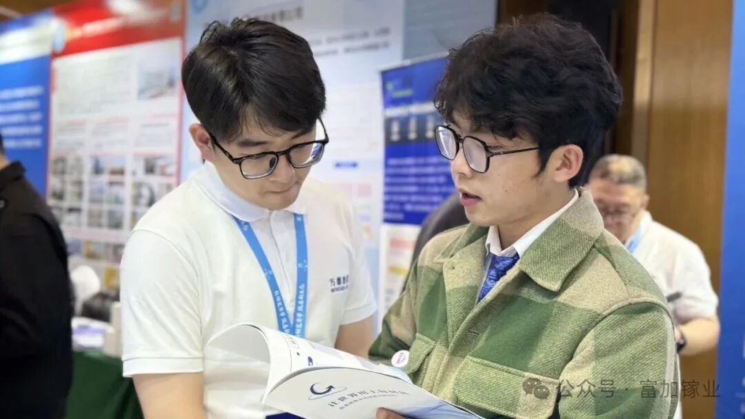
At this conference, Fujia Gallium systematically presented its latest industrialization achievements across the entire value chain of Gallium Oxide—from single-crystal growth to epitaxy and device fabrication. The exhibits covered multi-size Gallium Oxide substrates, high-quality homoepitaxial wafers, and core crystal growth equipment, comprehensively demonstrating the company’s vertically integrated capabilities spanning equipment, materials, epitaxy, and devices. The showcase attracted strong attention from research institutions, downstream device manufacturers, and industry experts.
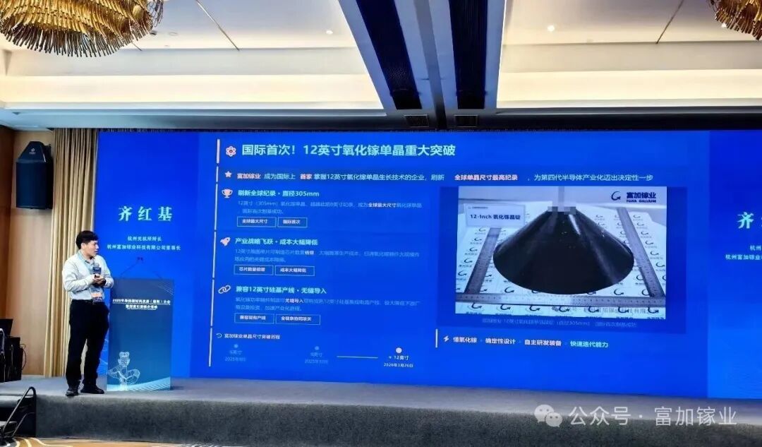
Chairman Qi Hongji Delivers Keynote: “Perspectives on the Industrialization of Fourth-Generation Semiconductor Gallium Oxide”
During the dedicated session on fourth-generation semiconductors, Researcher Qi Hongji was invited to deliver a keynote titled “Perspectives on the Industrialization of Fourth-Generation Semiconductor Gallium Oxide.” Drawing on years of experience in both research and industrialization, he provided a systematic analysis of Gallium Oxide development from multiple dimensions, including material growth technologies, industrial chain collaboration, and application scenarios.
Qi emphasized that Gallium Oxide, with its ultra-wide bandgap and high breakdown field, holds significant promise for high-performance power devices and has been explicitly included in China’s upcoming “15th Five-Year Plan.” However, the transition from laboratory research to large-scale industrialization still faces multiple challenges, such as large-diameter single-crystal growth, stability control of epitaxial processes, and the integration of device fabrication technologies. He also shared Fujia Gallium’s progress and practical experience in areas such as 12-inch single-crystal breakthroughs, intelligent crystal growth, homoepitaxy, as well as SBD wafer fabrication and device validation—offering valuable insights for the industry’s industrialization pathways.
Building a New Ecosystem, Shaping the Future Together
The 2026 Semiconductor New Materials Development (Deyang) Conference provided a high-level platform for exchange and collaboration across the industry. Looking ahead, Fujia Gallium will continue to uphold its vision of “bringing high-quality materials to the world,” deepen its focus on core Gallium Oxide technologies, and accelerate industrialization. The company aims to work closely with partners across the value chain to jointly promote the healthy development of the fourth-generation semiconductor ecosystem.
Product Portfolio
Gallium Oxide Crystal Growth Equipment
Fujia Gallium has developed the world’s first EFG crystal growth system featuring a proprietary “one-click crystal growth” function, supporting 2-inch to 6-inch crystal production. The system is protected by 6 granted domestic patents and 4 international patents. Complete equipment solutions and process packages are available.
The company has also independently developed fully automated VB (Vertical Bridgman) crystal growth equipment. It was the first in China to overcome the technical bottleneck of 6-inch single-crystal growth using the VB method, enabling large-diameter bulk crystal production. This platform is supported by 6 granted domestic patents and 4 international patents, with customizable equipment and process solutions available.
Gallium Oxide Single-Crystal Substrates
As one of China’s earliest pioneers in Gallium Oxide single-crystal research and an industry-leading supplier, Fujia Gallium provides high-quality single-crystal substrates to global customers.
The product portfolio includes 26 standard substrate specifications ranging from 2-inch to 6-inch diameters. Customized solutions are available in terms of wafer size, electrical properties, and crystal orientation, supporting both advanced epitaxy R&D and volume production requirements.
Gallium Oxide Epitaxial Wafers
Built upon mature MOCVD (Metal-Organic Chemical Vapor Deposition) and MBE (Molecular Beam Epitaxy) platforms, Fujia Gallium offers 15 standard epitaxial wafer products from 2-inch to 6-inch formats, as well as customized MBE-based epitaxial structures.
The company provides integrated “substrate + epitaxy” solutions. A precise process control system enables customization of key parameters including epitaxial layer thickness, doping concentration, and compositional uniformity, meeting diverse requirements across different power levels and device architectures.
About Hangzhou Fujia Gallium
Hangzhou Fujia Gallium Technology Co., Ltd., established on December 31, 2019, is committed to the vision of “enabling the world with better materials” and focuses on the industrialization of ultra-wide bandgap Gallium Oxide semiconductor materials. Its core products include Gallium Oxide single-crystal substrates, MOCVD/MBE epitaxial wafers, and crystal growth equipment based on the Vertical Bridgman (VB) and Edge-Defined Film-Fed Growth (EFG) methods. The company provides systematic solutions for material development, accelerating the integration of the entire ultra-wide bandgap Gallium Oxide industry chain and promoting the application of Gallium Oxide materials in power devices, microwave RF devices, and optoelectronic detection. A series of major achievements in Gallium Oxide development have been featured by leading media outlets including CCTV-1, CCTV-2, People’s Daily, Xinhua News Agency, China Securities Journal, and The Paper.
In terms of corporate recognition, the company was designated as a Zhejiang Province Science and Technology SME in 2022, recognized as a National High-Tech Enterprise in 2023, and awarded the titles of Hangzhou High-Tech Enterprise R&D Center and Zhejiang “Specialized and Sophisticated” SME in 2024. In 2025, it obtained ISO 9001 Quality Management System certification (Certificate No. 20225Q20294R0M) and was also named a 2024 Hangzhou “New Eagle” Enterprise. In the Gallium Oxide field, the company is leading the drafting of the first national standard in this area and has undertaken one project from the National Development and Reform Commission and one from the Ministry of Industry and Information Technology, while participating in three additional national and provincial-level projects supported by the National Natural Science Foundation of China and regional authorities in Zhejiang and Shanghai. To date, the company has been granted 14 international patents (6 in the United States, 7 in Japan, and 1 in Europe), 42 domestic patents, three registered “Fujia Gallium” trademarks, and five software copyrights, including its proprietary “One-Click Crystal Growth” control software.
