Paper Sharing
【Member Papers】Recent Breakthroughs in Gallium Oxide-Based Optoelectronic Devices for Neuromorphic Computing
日期:2026-04-21阅读:85
Researchers from the “Faculty of Infor-X, Xidian University; State Key Laboratory of Wide-Bandgap Semiconductor Devices and Integrated Technology, Xidian University, etc.” have published a dissertation titled "Recent Breakthroughs in Gallium Oxide-Based Optoelectronic Devices for Neuromorphic Computing" in Advanced Functional Materials.
Background
Driven by artificial intelligence (AI) and Internet of Things (IoT), the limitations of traditional von Neumann architecture—especially the “memory wall” and “power wall”—have become increasingly prominent due to the separation of memory and computing units. Neuromorphic computing has emerged as a promising paradigm by mimicking the structure and operation of the human brain, which achieves efficient information processing through approximately neurons and synaptic connections with low energy consumption and parallel processing capabilities.
Gallium oxide (Ga₂O₃), as an ultra-wide bandgap semiconductor (~4.9 eV), has attracted significant attention due to its excellent thermal stability, chemical inertness, and radiation resistance. Importantly, its abundant defect states (e.g., oxygen vacancies) can be dynamically modulated under optical and electrical stimuli, enabling synaptic-like behaviors. Additionally, its intrinsic ultraviolet response enables solar-blind detection, reducing interference from ambient light.
Recent advances in Ga₂O₃-based memristors, phototransistors, and photodetectors demonstrate various synaptic plasticity behaviors such as STP, LTP, and LTD. These devices show great potential in applications including image recognition, information security, and biomimetic perception, providing a foundation for integrated sensing-memory-computing systems.
Abstract
Driven by artificial intelligence (AI) and Internet of Things (IoT) technologies, the “memory wall” and “power wall” issues of the traditional von Neumann architecture have become increasingly prominent. Neuromorphic computing has emerged as a crucial breakthrough direction due to its advantages of imitating the human brain’s in-memory computing and low power consumption, with synaptic devices being its core component. As a wide-bandgap semiconductor, gallium oxide (Ga₂O₃) possesses excellent thermal stability, chemical inertness, and radiation resistance. Moreover, its abundant defect states (e.g., oxygen vacancies) can be dynamically modulated via light and electrical stimuli, enabling Ga₂O₃-based devices to exhibit synaptic-like behaviors, thus making it an ideal material for simulating biological synapses. This review systematically examines cutting-edge developments in Ga₂O₃-based optoelectronic devices for neuromorphic computing applications. First, this paper provides a comprehensive overview of the behaviors of biological synapses. Subsequently, it introduces the operating principles and core device performance metrics of Ga₂O₃-based memristors, phototransistors, and photodetectors for neuromorphic computing. Finally, the synaptic plasticity of Ga₂O₃ optoelectronic devices and their applications in neuromorphic computing were summarized, providing a material-device-system full-architecture solution for the next generation of neuromorphic chips.
Highlights
Material advantage: ultra-wide bandgap and defect engineering:Ga₂O₃ enables dual-mode modulation via abundant defect states
Device diversity:Includes memristors, phototransistors, and photodetectors
Strong synaptic plasticity emulation:Demonstrates STP, LTP, LTD, PPF, and STDP
Optoelectronic synergy:Combines optical pre-activation with electrical modulation
Wide application scope:Image recognition, security, biomimetic behaviors
System-level integration:Provides full-stack neuromorphic architecture solution
Conclusion
Ga₂O₃-based optoelectronic devices demonstrate great potential in neuromorphic computing, comprehensively simulating the functional characteristics of human neuronal synapses through electrical, optical, and optoelectronic synergistic modes. The team believes their core advantage lies in achieving high functional equivalence with biological synapses through intrinsic physical processes, without complex external circuit control. This not only simplifies the architecture of neuromorphic systems but also endows them with biological-level adaptability and integration capabilities. Optoelectronic synergy offers flexible multimodal solutions for building neuromorphic systems with efficient information processing capabilities.
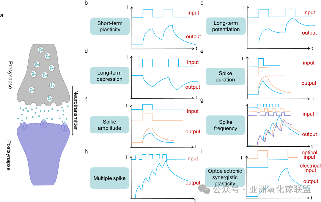
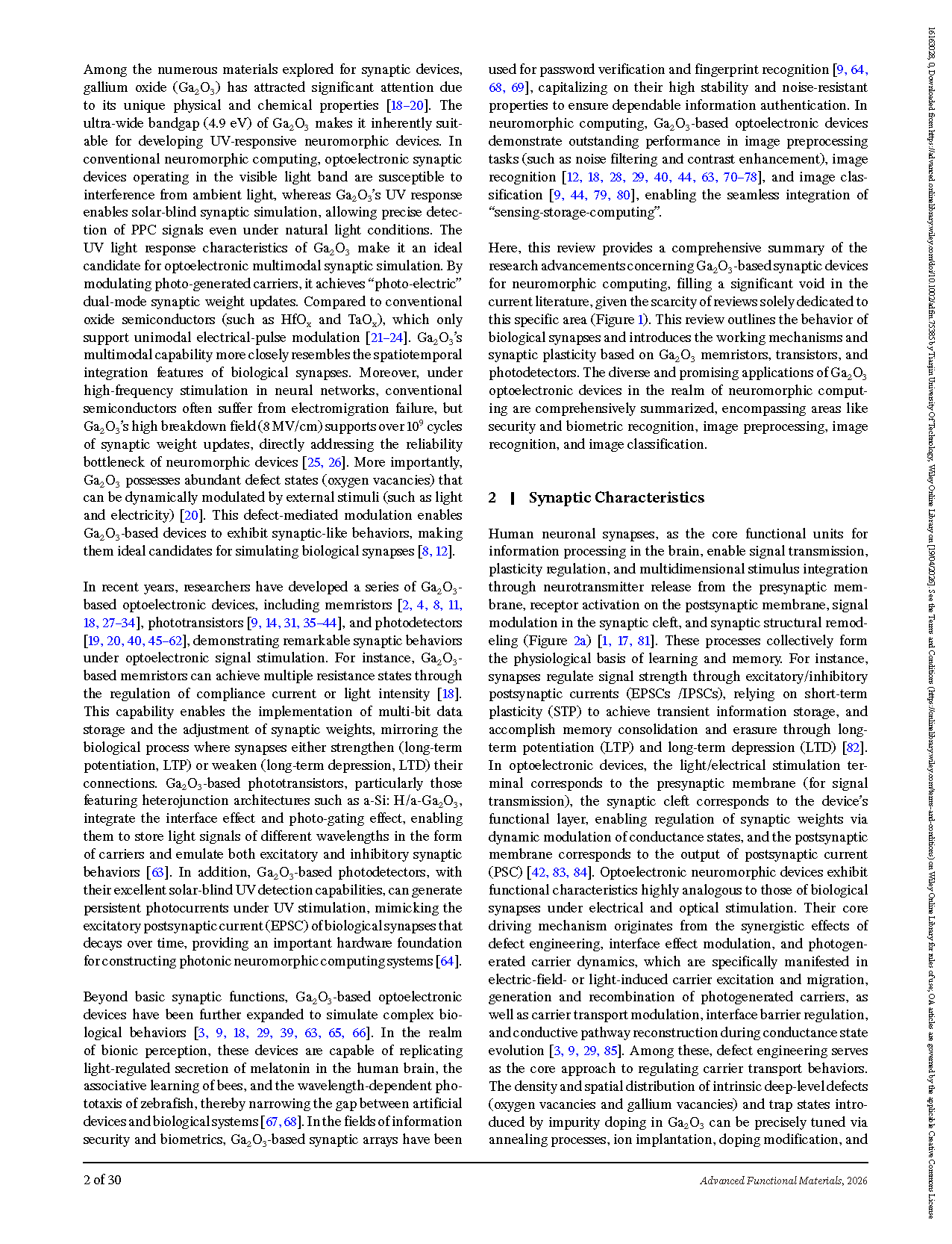
FIGURE 1 Framework of Ga₂O₃ optoelectronic devices for neuromorphic computing: material properties, optoelectronic synapse, biological synapse, and neuromorphic computing.
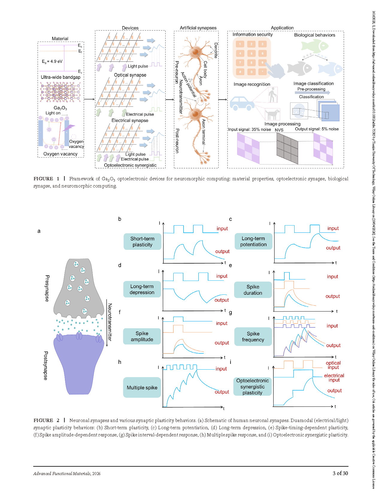
FIGURE 2 Neuronal synapses and various synaptic plasticity behaviors. (a) Schematic of human neuronal synapses. Duamodal (electrical/light) synaptic plasticity behaviors: (b) Short-term plasticity, (c) Long-term potentiation, (d) Long-term depression, (e) Spike-timing-dependent plasticity, (f) Spike amplitude-dependent response, (g) Spike interval-dependent response, (h) Multiple spike response, and (i) Optoelectronic synergistic plasticity.
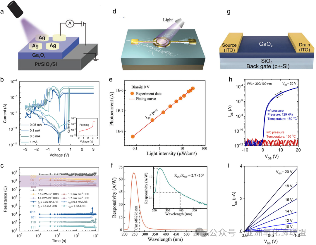
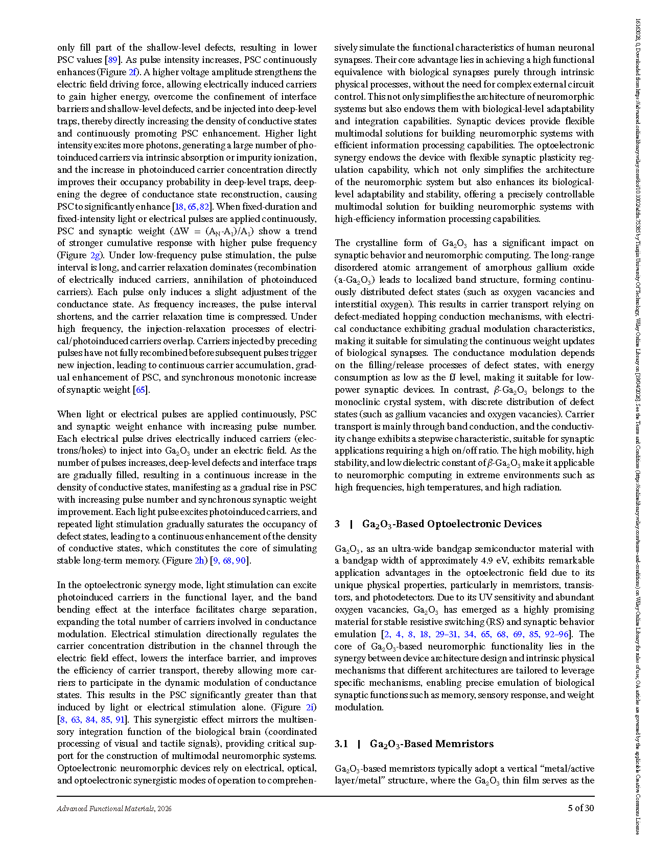
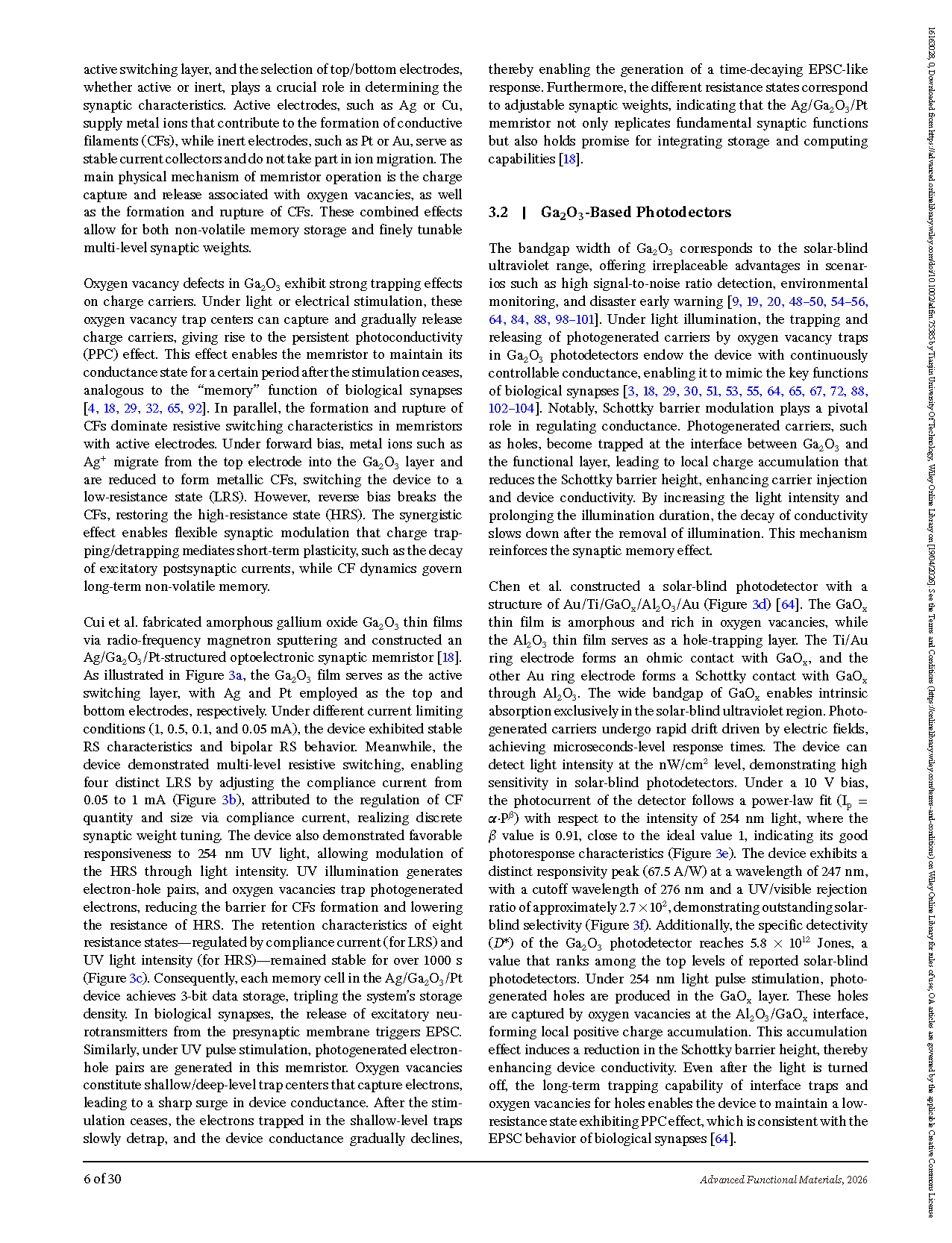
FIGURE 3 Ga₂O₃ electronic devices. (a) Structural diagram of the Ag/Ga₂O₃/Pt memristor. (b) Typical I–V curves of the memristor under different Icc. (c) The retention characteristics of the memristor. (d) Structural diagram of the Ga₂O₃-based photodetector. (e) The plot of photocurrent versus light intensity of the photodetector. (f) The spectral responsivity characteristics of the photodetector and its corresponding curve are plotted on logarithmic scales. (g) Structural diagram of Ga₂O₃-based transistor. (h) The transfer characteristic curve of the transistor. (i) The output characteristic curve of the transistor.
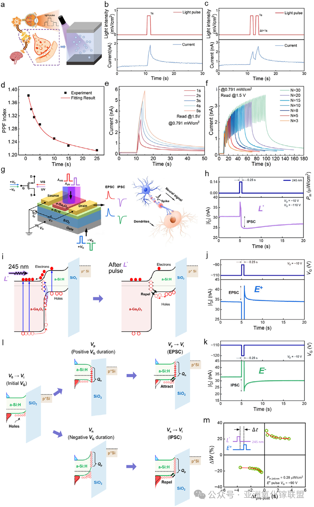
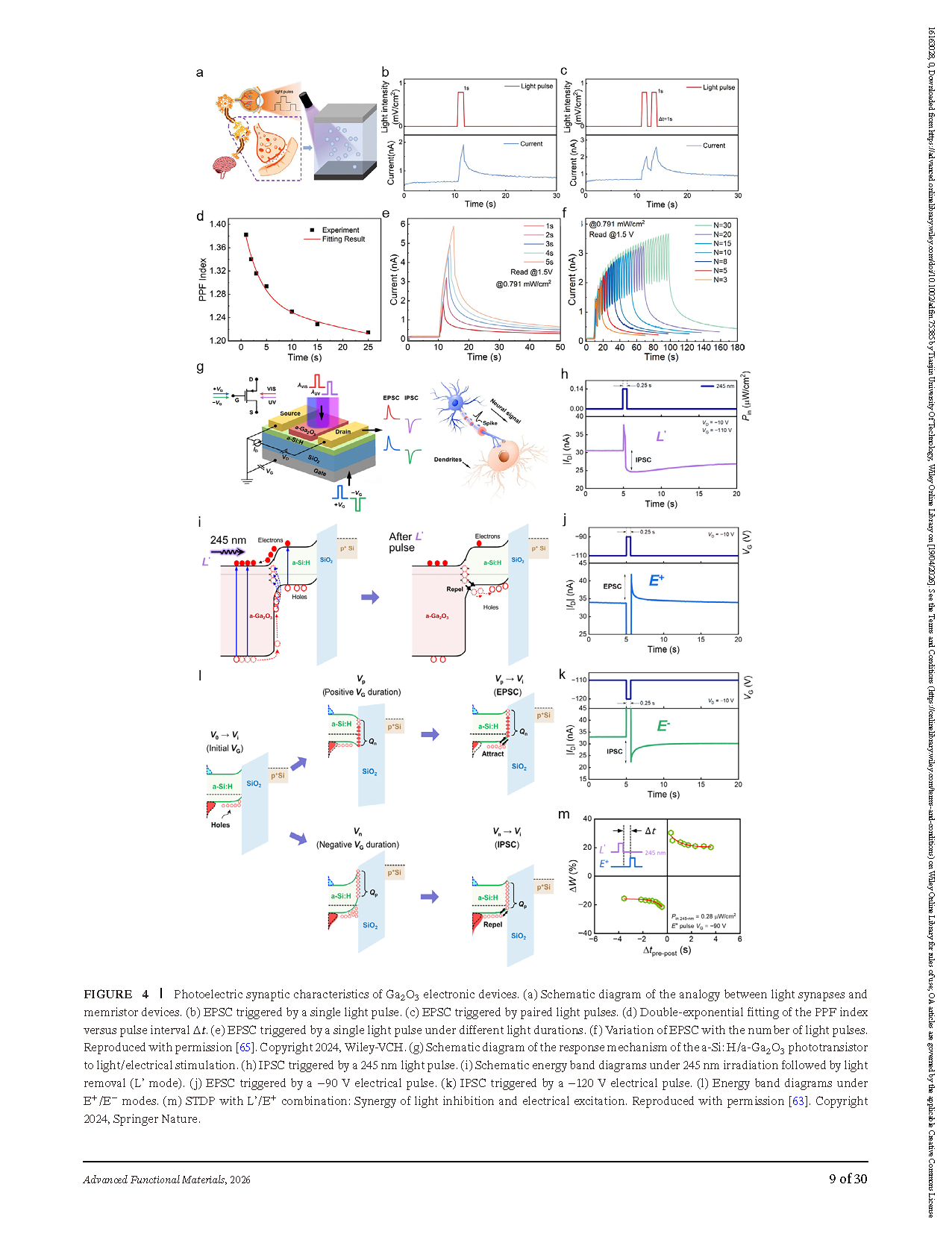
FIGURE 4 Photoelectric synaptic characteristics of Ga₂O₃ electronic devices. (a) Schematic diagram of the analogy between light synapses and memristor devices. (b) EPSC triggered by a single light pulse. (c) EPSC triggered by paired light pulses. (d) Double-exponential fitting of the PPF index versus pulse interval Δt. (e) EPSC triggered by a single light pulse under different light durations. (f) Variation of EPSC with the number of light pulses. (g) Schematic diagram of the response mechanism of the a-Si: H/a-Ga₂O₃ phototransistor to light/electrical stimulation. (h) IPSC triggered by a 245 nm light pulse. (i) Schematic energy band diagrams under 245 nm irradiation followed by light removal (L’ mode). (j) EPSC triggered by a −90 V electrical pulse. (k) IPSC triggered by a −120 V electrical pulse. (l) Energy band diagrams under E+/E− modes. (m) STDP with L’/E+ combination: Synergy of light inhibition and electrical excitation.
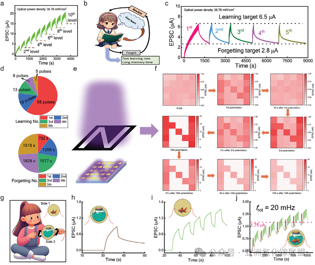
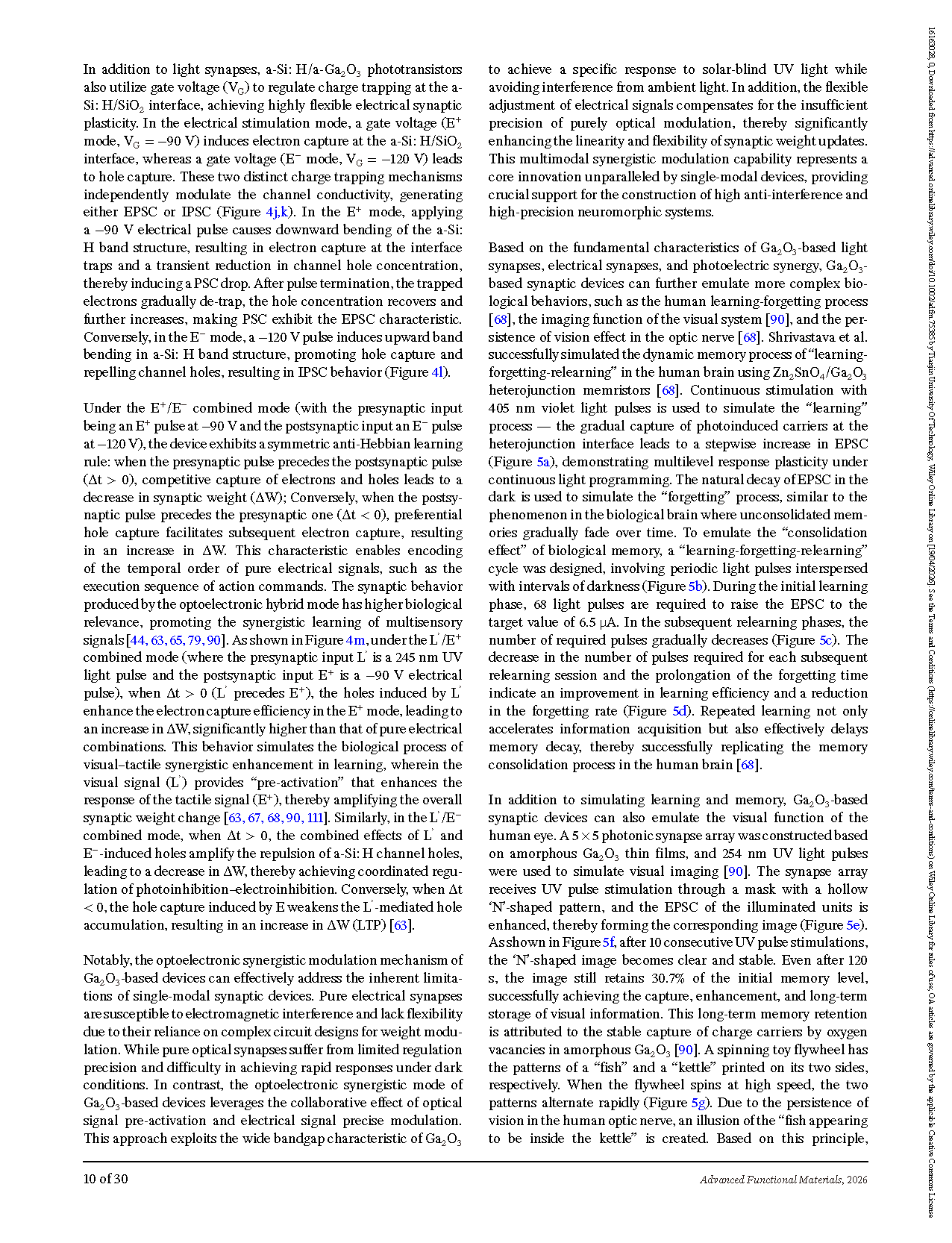
FIGURE 5 Biological synaptic plasticity simulation. (a) Multi-level EPSC response under continuous light programming. (b) Schematic illustration of “learning-forgetting-relearning” behavior. (c) Five-cycle repetition of the learning and forgetting process. (d) Quantitative relationship between (re)learning/forgetting cycles and required pulse number/decay time. (e) Schematic diagram of an imaging system based on a synaptic array. (f) Output images of the synaptic array after ten consecutive UV pulse stimulations. (g) Schematic of a rotating flywheel toy with “fish” and “kettle” patterns on both sides. EPSC responses corresponding to the “water-pot” (h) and the “fish” (i). (j) EPSC characteristics of the device under 20 mHz rotation frequency stimulation.
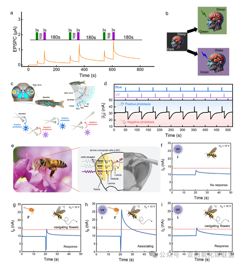
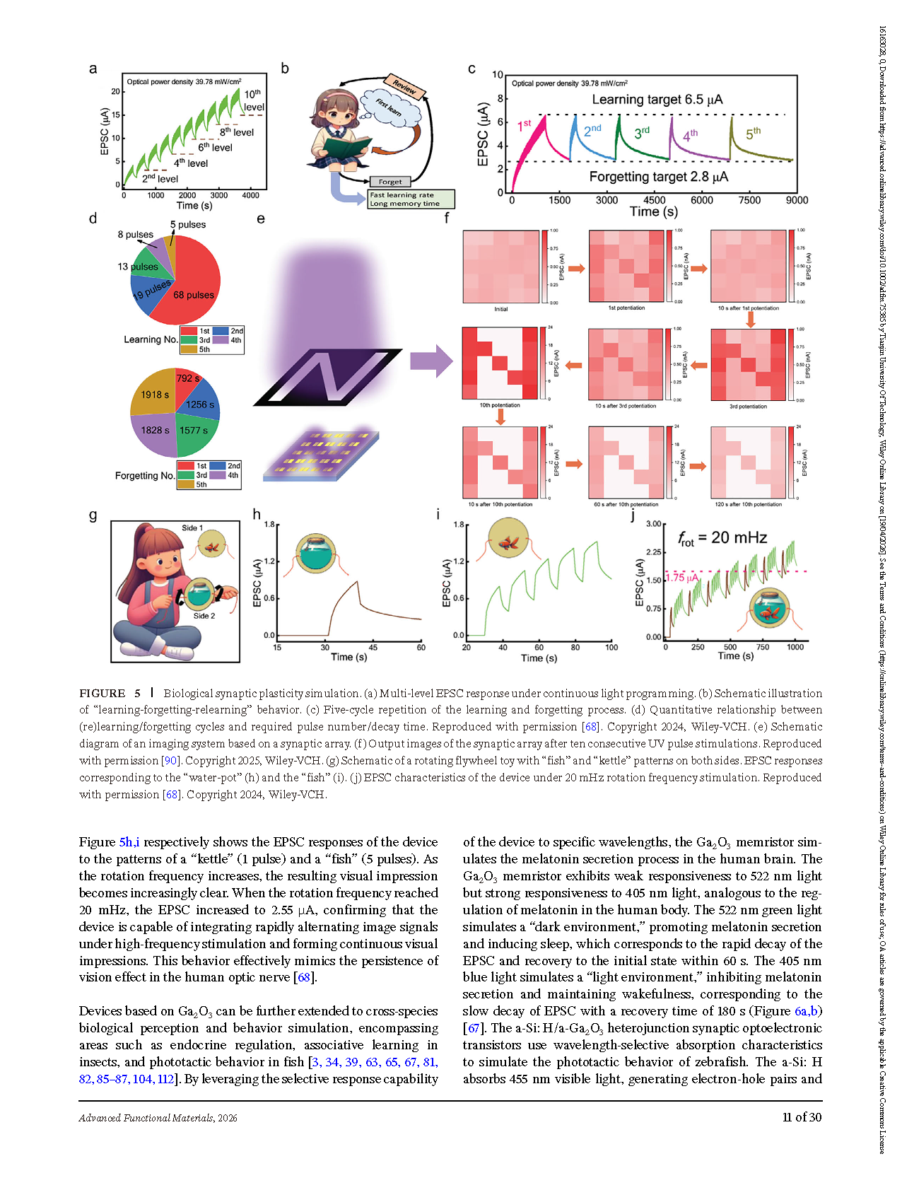
FIGURE 6 Biological synaptic plasticity simulation. (a) The PSC alteration of the Ga₂O₃ memristor under the illumination of 522 and 405 nm light. (b) Schematic illustration of melatonin secretion and inhibition at green light and blue light. (c) Diagram of the zebrafish visual nervous system, positive and negative phototaxis behaviors. (d) Simulation results of color-dependent behavior. (e) Image of a bee on flowers and the basic characteristics of color processing in the bee brain. (f) EPSC induced by UV light stimulation. (g) EPSC induced by voltage stimulation, resulting in UR generation. (h) EPSC induced by the combined UV light and voltage stimulation, establishing a conditioned association. (i) UR generation via UV light stimulation alone post combined training.
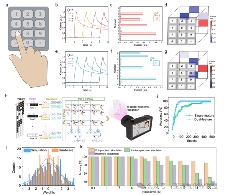
FIGURE 7 Applications of neuromorphic computing in security and biometric recognition. (a) 3 × 4 pixel array defined to represent numerals (0–9) and symbols (“*” and “#”) for password input. (b) Current values of the numbers “4, 2, 6, 9” pixels under sequential light pulse stimulation at different time points. (c) Current output, and (d) 2D mapping for the incorrect password “4, 2, 6, 9”. (e) Current values of the numerals “0, 5, 1, 9” pixels under sequential light pulse stimulation at different time points. (f) Current output, and (g) 2D mapping for the correct password “0 5 1 9”. (h) Schematic diagram of the fingerprint recognition system. (i) Evolution of accuracy during readout network training for single- and dual-feature-based recognition. (j) Statistical histograms of 40×5 weights from simulations and hardware experiments, respectively. (k) Effect of stochastic noise on recognition accuracy for fingerprint recognition in the RC system.
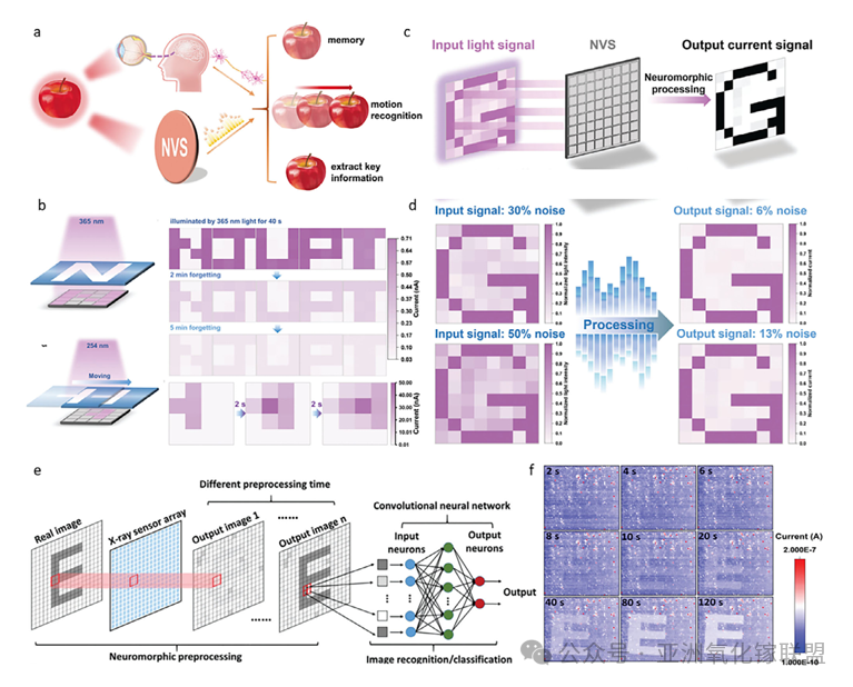
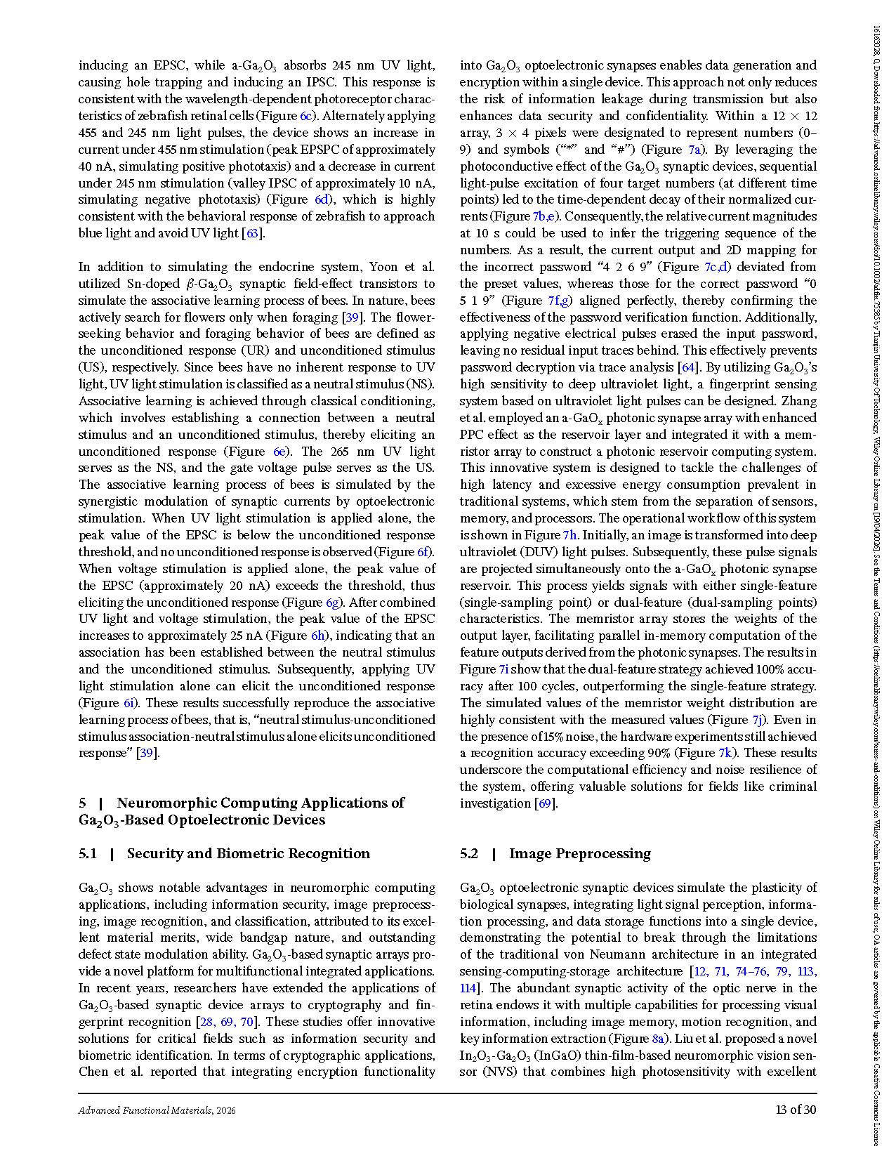
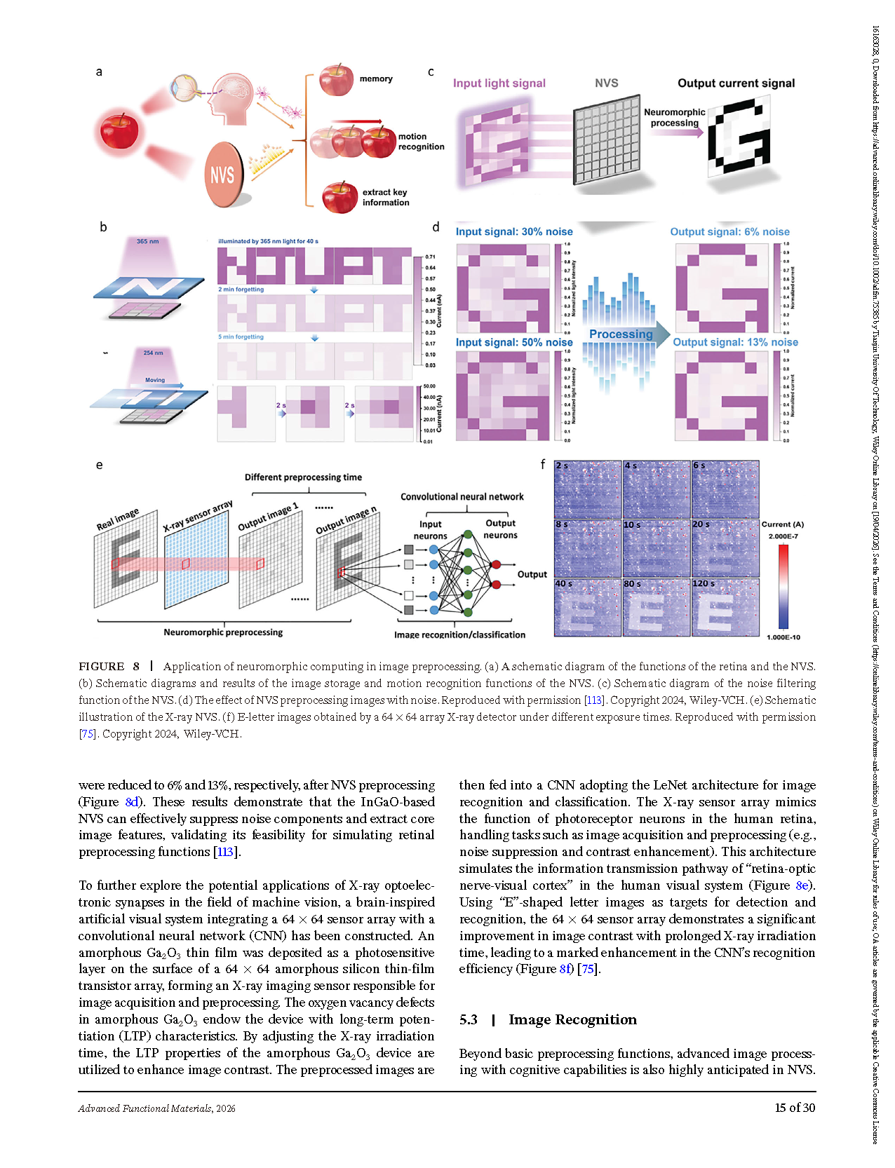
FIGURE 8 Application of neuromorphic computing in image preprocessing. (a) A schematic diagram of the functions of the retina and the NVS. (b) Schematic diagrams and results of the image storage and motion recognition functions of the NVS. (c) Schematic diagram of the noise filtering function of the NVS. (d) The effect of NVS preprocessing images with noise.
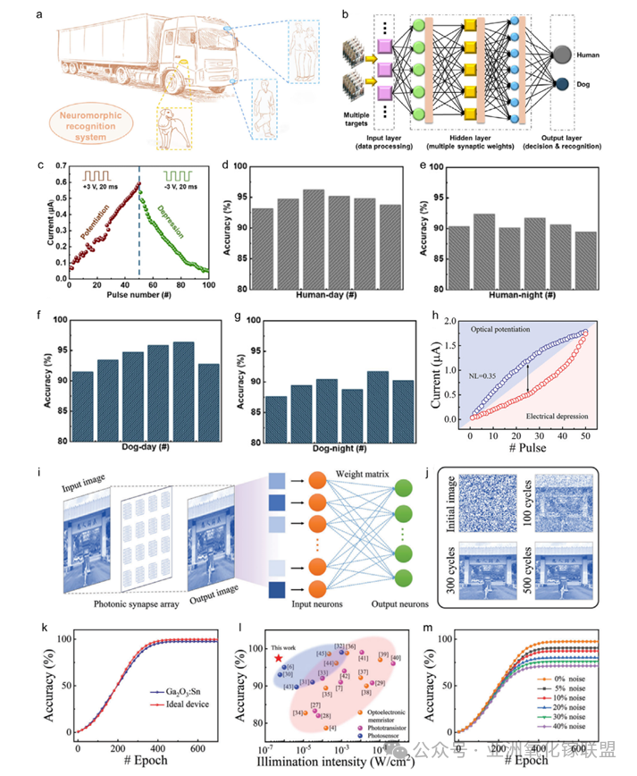
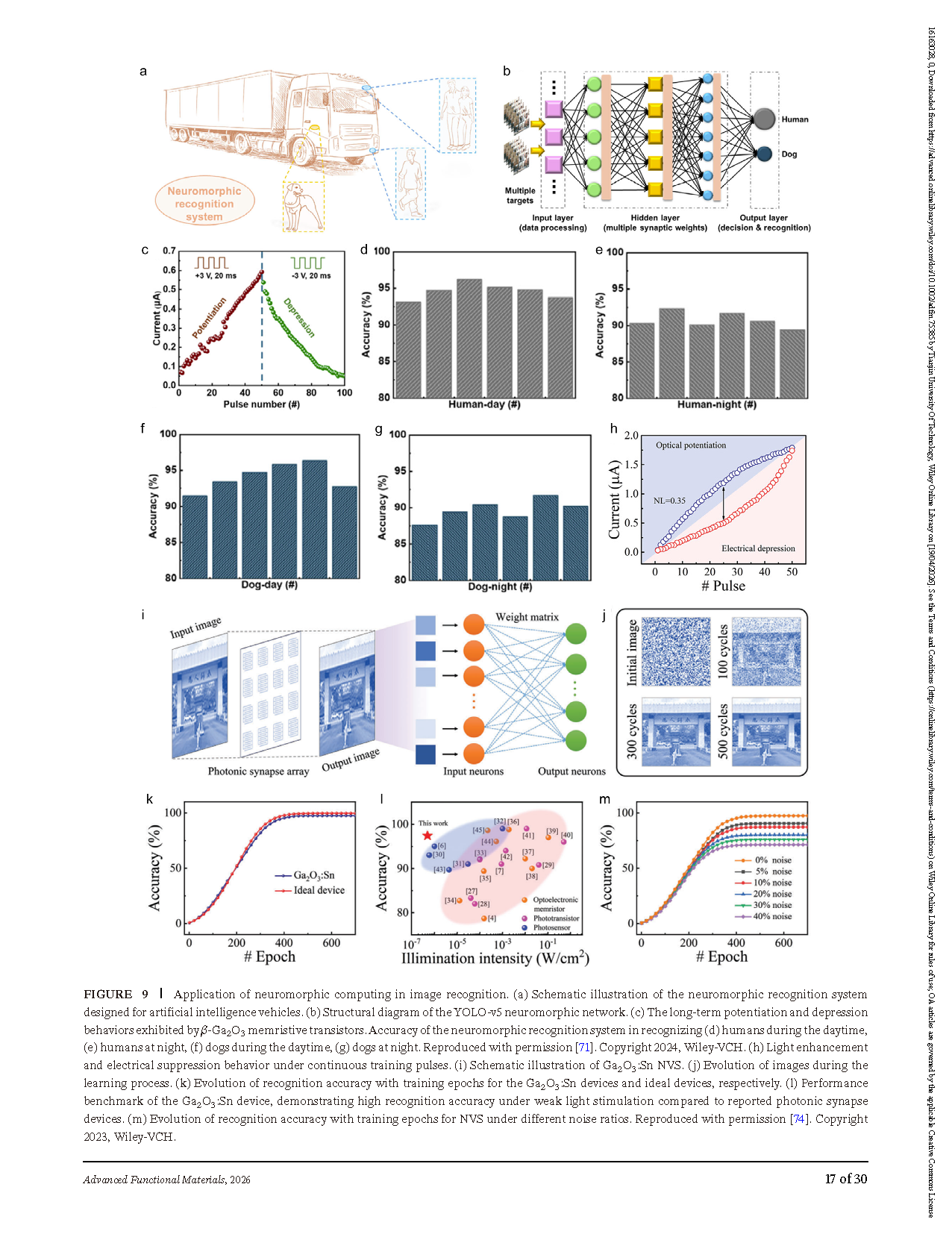
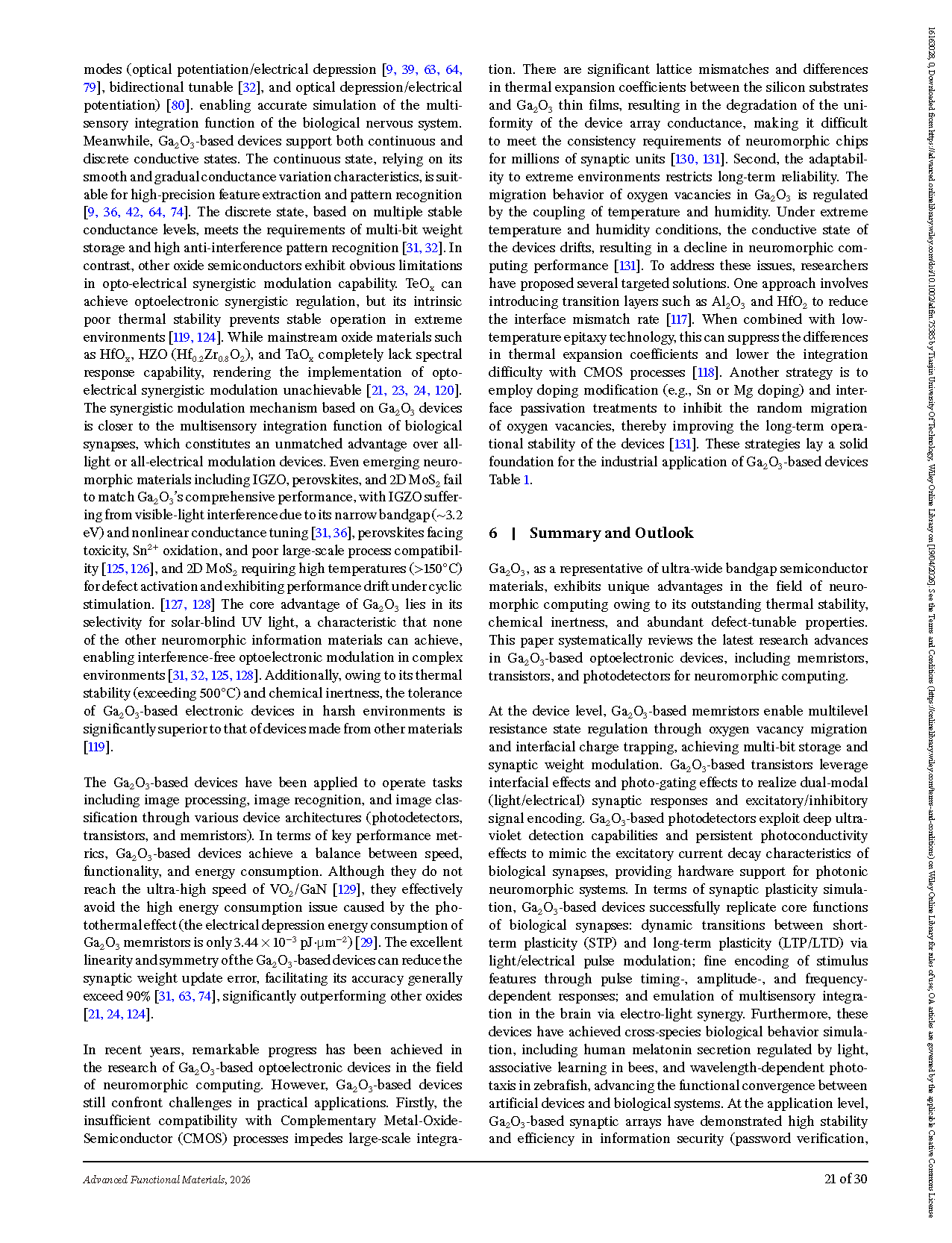
FIGURE 9 Application of neuromorphic computing in image recognition. (a) Schematic illustration of the neuromorphic recognition system designed for artificial intelligence vehicles. (b) Structural diagram of the YOLO-v5 neuromorphic network. (c) The long-term potentiation and depression behaviors exhibited by β-Ga₂O₃ memristive transistors. Accuracy of the neuromorphic recognition system in recognizing (d) humans during the daytime, (e) humans at night, (f) dogs during the daytime, (g) dogs at night. (h) Light enhancement and electrical suppression behavior under continuous training pulses. (i) Schematic illustration of Ga₂O₃:Sn NVS. (j) Evolution of images during the learning process. (k) Evolution of recognition accuracy with training epochs for the Ga₂O₃:Sn devices and ideal devices, respectively. (l) Performance benchmark of the Ga₂O₃:Sn device, demonstrating high recognition accuracy under weak light stimulation compared to reported photonic synapse devices. (m) Evolution of recognition accuracy with training epochs for NVS under different noise ratios.
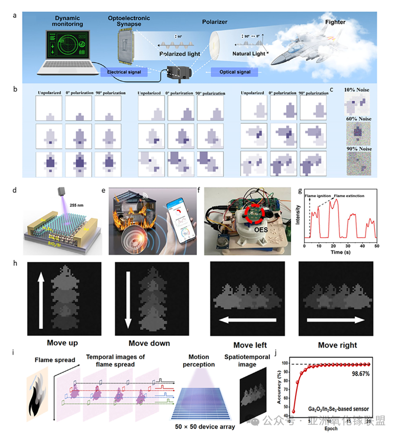
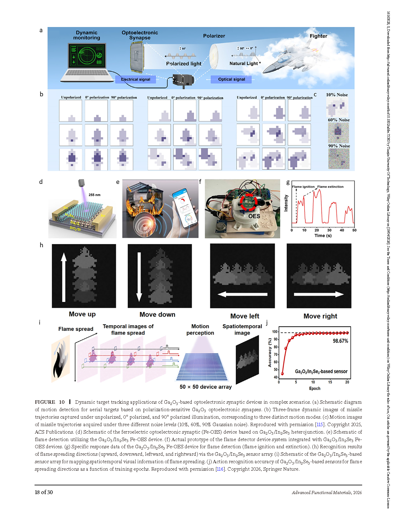
FIGURE 10 Dynamic target tracking applications of Ga₂O₃-based optoelectronic synaptic devices in complex scenarios. (a) Schematic diagram of motion detection for aerial targets based on polarization-sensitive Ga₂O₃ optoelectronic synapses. (b) Three-frame dynamic images of missile trajectories captured under unpolarized, 0° polarized, and 90° polarized illumination, corresponding to three distinct motion modes. (c) Motion images of missile trajectories acquired under three different noise levels (10%, 60%, 90% Gaussian noise). (d) Schematic of the ferroelectric optoelectronic synaptic (Fe-OES) device based on Ga₂O₃/In₂Se₃ heterojunction. (e) Schematic of flame detection utilizing the Ga₂O₃/In₂Se₃ Fe-OES device. (f) Actual prototype of the flame detector device system integrated with Ga₂O₃/In₂Se₃ Fe-OES devices. (g) Specific response data of the Ga₂O₃/In₂Se₃ Fe-OES device for flame detection (flame ignition and extinction). (h) Recognition results of flame spreading directions (upward, downward, leftward, and rightward) via the Ga₂O₃/In₂Se₃ sensor array. (i) Schematic of the Ga₂O₃/In₂Se₃-based sensor array for mapping spatiotemporal visual information of flame spreading. (j) Action recognition accuracy of Ga₂O₃/In₂Se₃-based sensors for flame spreading directions as a function of training epochs.
DOI:
doi.org/10.1002/adfm.75385