


Member News
【Member News】GAREN Semiconductor Showcases at the China New-Quality Semiconductor Innovation 30th Anniversary Exhibition: Leading a New Chapter in China’s Gallium Oxide Industry Through Full-Chain Innovation
日期:2026-04-24阅读:328
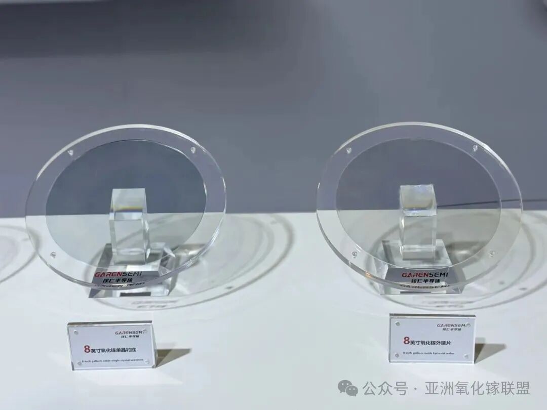
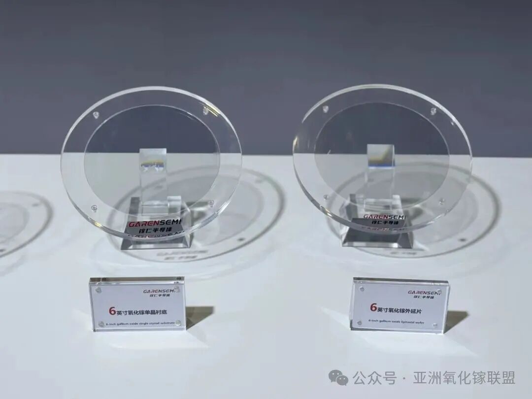
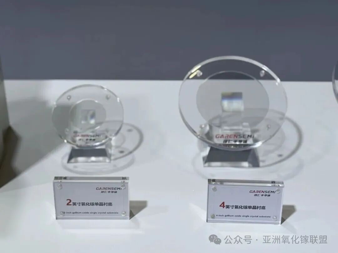
On April 23, 2026, the “30th Anniversary Special Exhibition on China’s New-Quality Semiconductor Innovation and Development” grandly opened, drawing significant attention from across the industry. Hangzhou GAREN Semiconductor Co., Ltd. (hereinafter referred to as “GAREN”) made a prominent appearance, showcasing its globally debuted 8-inch Gallium Oxide epitaxial wafer, a full range of Gallium Oxide single-crystal substrates, and dedicated VB-method crystal growth equipment.
The exhibition highlighted GAREN’s core achievements in fourth-generation semiconductor Gallium Oxide, demonstrating the company’s strong technological capabilities and underscoring the innovative breakthroughs made by Chinese enterprises in the ultra-wide bandgap semiconductor field.
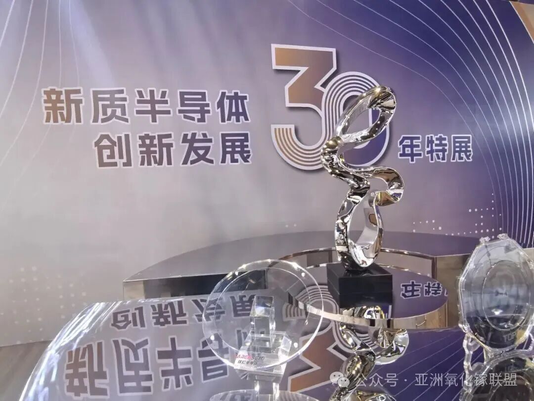
Figure 1 GAREN Semiconductor products on display
“30th Anniversary Special Exhibition on China’s New-Quality Semiconductor Innovation and Development”
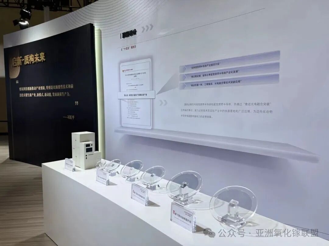
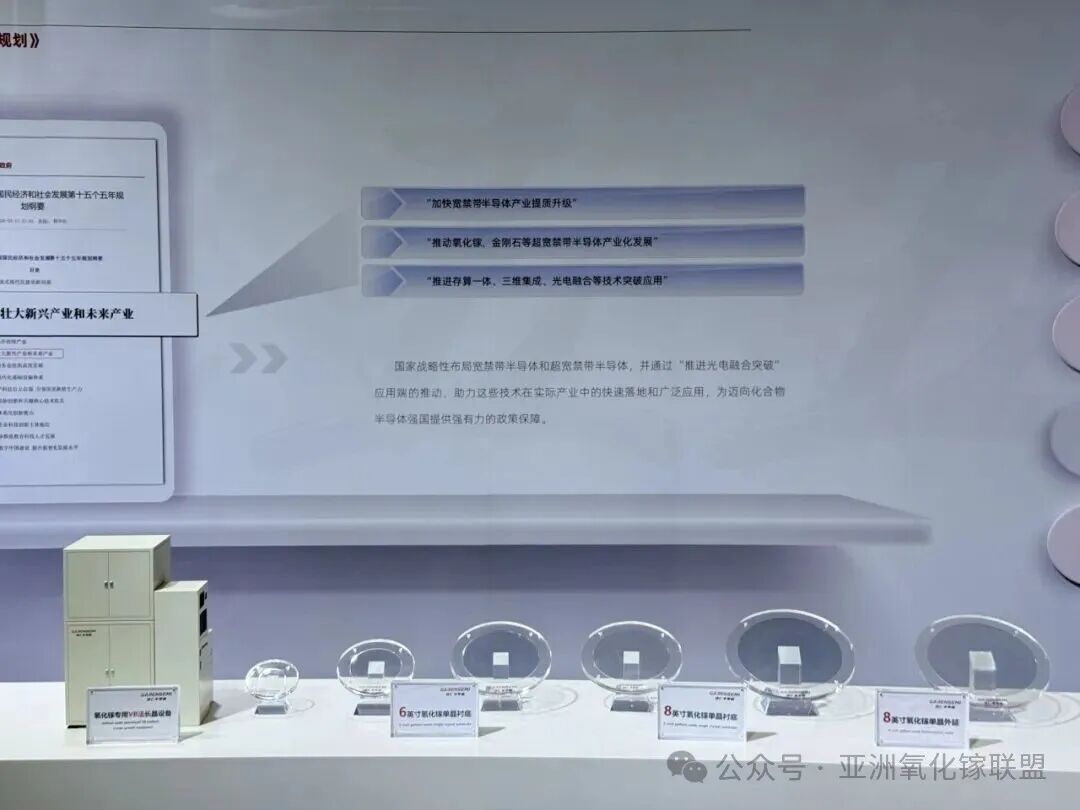
Figure 2 Full product lineup of GAREN Semiconductor
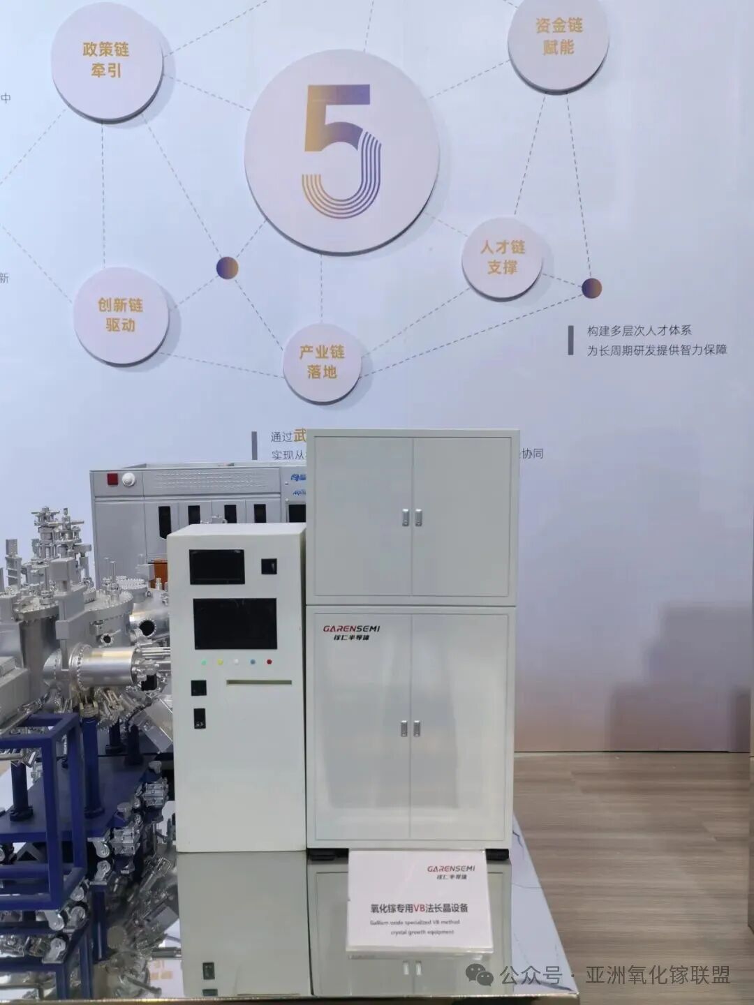
Figure 3 Booth of GAREN Semiconductor’s VB-method crystal growth equipment for Gallium Oxide
Full-Chain Strength, Global Leadership
From 2025 to 2026, GAREN Semiconductor has continued to make sustained advances in the field of Gallium Oxide, achieving multiple key breakthroughs.
On the technology front, the company has repeatedly pushed the limits of crystal size—globally launching 8-inch Gallium Oxide single crystals via casting in 2025, followed by the world’s first 8-inch homoepitaxial Gallium Oxide wafers in 2026—maintaining a leading position in large-size material fabrication. At the same time, GAREN has steadily advanced multiple process routes. Its self-developed VB crystal growth equipment for Gallium Oxide has been fully commercialized, enabling domestic substitution of core equipment and forming an integrated technological loop spanning equipment–substrate–epitaxy.
On the industrial front, supported by a mature technology system and proprietary equipment, GAREN Semiconductor has realized scalable mass production of Gallium Oxide substrates and epitaxial wafers across multiple sizes. Both its 8-inch substrates and homoepitaxial wafers have demonstrated outstanding performance in authoritative testing. The company has established stable batch delivery capabilities and provides key material support to leading device manufacturers worldwide. In addition, its independently developed high-quality semi-insulating Gallium Oxide substrates have enabled the Shenzhen Pinghu Laboratory to successfully develop kV-class ultra-low on-resistance Gallium Oxide photoconductive switches, accelerating the transition of Gallium Oxide from laboratory research to industrial application.
Taking Responsibility to Strengthen China’s Semiconductor Industry
At present, China’s “15th Five-Year Plan” explicitly calls for promoting the industrialization of ultra-wide bandgap semiconductors such as Gallium Oxide and diamond, elevating the industry to a national strategic priority.
GAREN Semiconductor’s achievements represent a concrete response to this national strategy and a deep commitment to the Gallium Oxide industry. From independent development of core equipment to breakthroughs in key materials, the company continues to inject strong momentum into the high-quality development of China’s Gallium Oxide sector. Its advances in large-size materials and core equipment provide valuable industrialization experience, elevate overall technological standards, and help drive China’s transition from a follower to a parallel runner—and ultimately a leader—in the fourth-generation semiconductor race.
Notably, GAREN Semiconductor was selected as the only Gallium Oxide company representing fourth-generation semiconductors in the large-scale documentary “New-Quality Chip Power”. Premiered during this special exhibition, the documentary features interviews with leading academicians, experts, and entrepreneurs, offering a comprehensive record of China’s compound semiconductor innovation journey. GAREN’s inclusion not only reflects strong industry recognition of its technological and industrial contributions, but also highlights the growing global significance of China’s fourth-generation semiconductor enterprises.
Looking ahead, the company will accelerate device validation and production line integration for 6-inch and 8-inch epitaxial wafers, contributing further to the high-quality development of China’s advanced semiconductor industry and strengthening its position in global competition.
About GAREN SEMI
Hangzhou Garen Semiconductor Co., Ltd. is a world-leading provider of Gallium Oxide materials and equipment solutions, focusing on R&D and industrialization in the ultra-wide bandgap semiconductor field. The company’s core products include 2–8-inch Gallium Oxide single crystals and substrates (with 8-inch being the world’s first), Gallium Oxide Vertical Bridgman (VB) crystal growth equipment, Gallium Oxide epitaxial wafers, etc. It is committed to building a full-chain product system of “equipment–crystal–substrate–epitaxy” to provide systematic solutions for global customers. The company’s achievements in Gallium Oxide have been specially reported by well-known media including People’s Daily, Xinhua News Agency, Science and Technology Daily, Sina Finance, China Blue News, and The Paper.
Enterprise Honors Summary
Recognized as a National-level Science and Technology Small and Medium-sized Enterprise and Zhejiang Innovative Small and Medium-sized Enterprise in 2023;Awarded Zhejiang Specialized, Sophisticated, Unique and New Small and Medium-sized Enterprise in 2024;Approved as a High-tech Enterprise in 2025;Won the SEMI Outstanding Contribution Award for Sustainable Development at SEMICON CHINA 2025, the Together Progress Award at the Jufeng Summit Forum (JFSC) and Compound Semiconductor Industry Expo, the Innovation Vitality Award of Zhejiang Semiconductor Industry, the Second Prize in the Enterprise Group of the 10th “Maker China” Zhejiang Provincial Finals, the Top 500 Enterprise Group of the 10th “Maker China” SME Innovation and Entrepreneurship Competition, and the 2024–2025 Semiconductor Material Industry Contribution Award;The major breakthrough in the preparation of 8-inch Gallium Oxide single crystals and substrates was selected as one of the “Top 10 Advances in China’s Third-Generation Semiconductor Technology 2025” and “Major Scientific and Technological Achievements 2025” by the Department of Science and Technology of Zhejiang Province;Led the formulation of 2 group standard drafts, participated in drafting 1 national standard, and participated in promoting 1 group standard draft in the Gallium Oxide field;Supported by the “5213” Excellence Program of Xiaoshan District, Hangzhou, Zhejiang Province, and approved to establish Zhejiang Enterprise Research Institute;Obtained the quality management system certification;Granted 14 authorized invention patents at home and abroad (including patents in the US, Japan and other countries), with more than 50 patents pending.
For more information about Garen Semiconductor and its products, please visit our official website: http://garen.cc/
Or contact us via the following ways:
Mr. Jiang: 15918719807
E-mail: jiangjiwei@garen.cc
Mr. Xia: 19011278792
E-mail: xianing@garen.cc
