Paper Sharing
【Domestic Papers】Direct Bulk β-Ga₂O₃ Crystals Growth of 4° Miscut (100) Primary Surfaces by Edge-defined Film-fed Growth Method
日期:2026-05-06阅读:181
Researchers from Shandong University have published a dissertation titled " Direct Bulk β-Ga2O3 Crystals Growth of 4° Miscut (100) Primary Surfaces by Edge-defined Film-fed Growth Method " in Journal of Alloys and Compounds.
Background
β-Ga2O3, an ultrawide-bandgap semiconductor, exhibits unique physical and chemical properties, making it highly promising for power electronics, solar-blind detection, and X-ray sensing. With a bandgap of 4.6–4.9 eV, it possesses a high theoretical breakdown field of 8 MV/cm and a Baliga’s figure of merit exceeding 3000. Among its various phases, the β-phase gallium oxide is the most stable and can be grown from the melt using methods such as Czochralski(Cz), edge-defined film-fed growth (EFG) method, Bridgman, and casting. β-Ga2O3 single-crystal substrates produced via melt growth methods offer high quality and large size, although their growth process requires the use of precious metals such as Ir or Pt–Rh. Therefore, well-developed growth processes are essential to reduce the substrate manufacturing cost. These excellent electrical properties and scalable growth techniques underscore strong potential of β-Ga2O3 as a commercial substrate for power devices like SBDs and MOSFETs, driving extensive research to further improve device performance. Achieving high-performance devices requires not only optimal device design but also high-quality epitaxial films characterized by low defect density, high crystallinity, and uniform thickness and doping.
Abstract
The strong anisotropy of monoclinic β-Ga2O3 leads to distinct growth behaviors during homoepitaxy on substrates of different orientations. Among these, a substrate orientation whit a 4° miscut from the (100) plane towards the [00-1] direction (4° miscut (100) plane) shows significant potential for growing high-quality epitaxial films. To enhance substrate preparation efficiency, this study employed the directional seed edge defined film-fed growth (EFG) method to directly grow β-Ga2O3 single crystal with a predominant 4° miscut (100) plane, clarifying the rationale for this specific orientation. Optimization of the growth process eliminated twin defects, yielding a high-quality 2 inch single crystal. A rocking curve of the polished substrate exhibited a full width at half maximum (FWHM) of 73.89 arcsec, which indicated high crystalline quality. UV vis transmission spectroscopy revealed a 4.52 eV band gap of the 4° miscut (100) plane, confirming its wide-bandgap feature. Wet etching was performed on the 4° miscut (100) plane, and the resulting etch pit morphology was revealed through observations by optical microscope and atomic force microscope (AFM). Overall, the 4° miscut (100) β-Ga2O3 single crystal grown by the EFG method demonstrate excellent properties, making them promising for substrate preparation, homoepitaxy, and device fabrication.
Conclusion
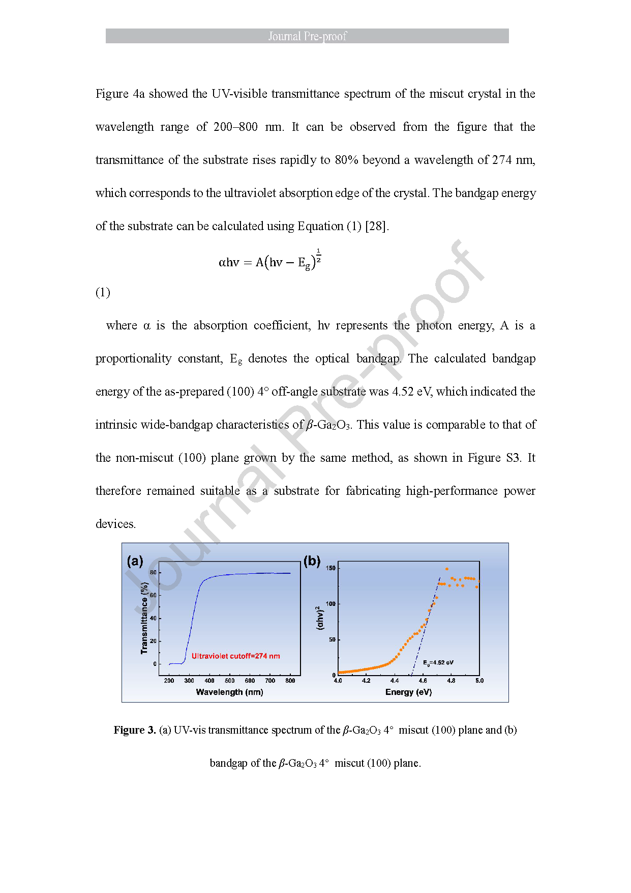
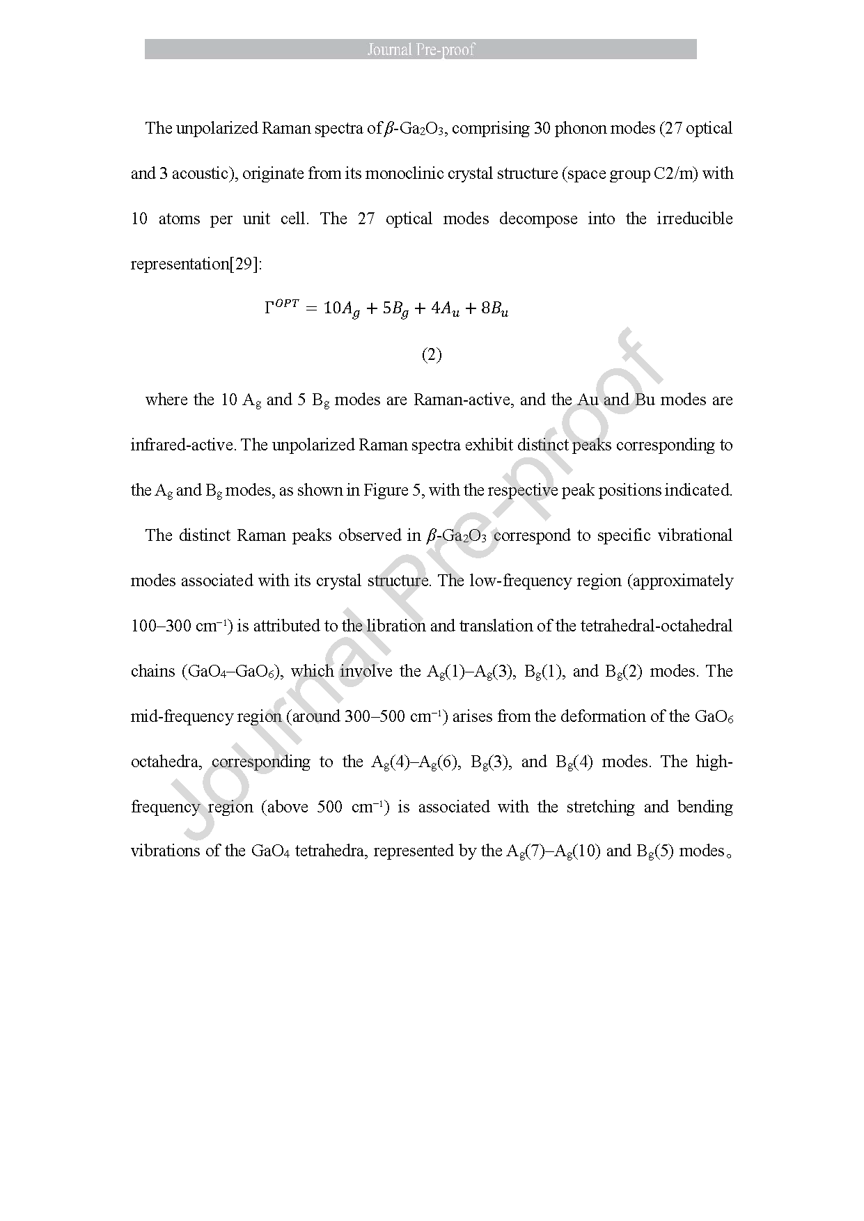
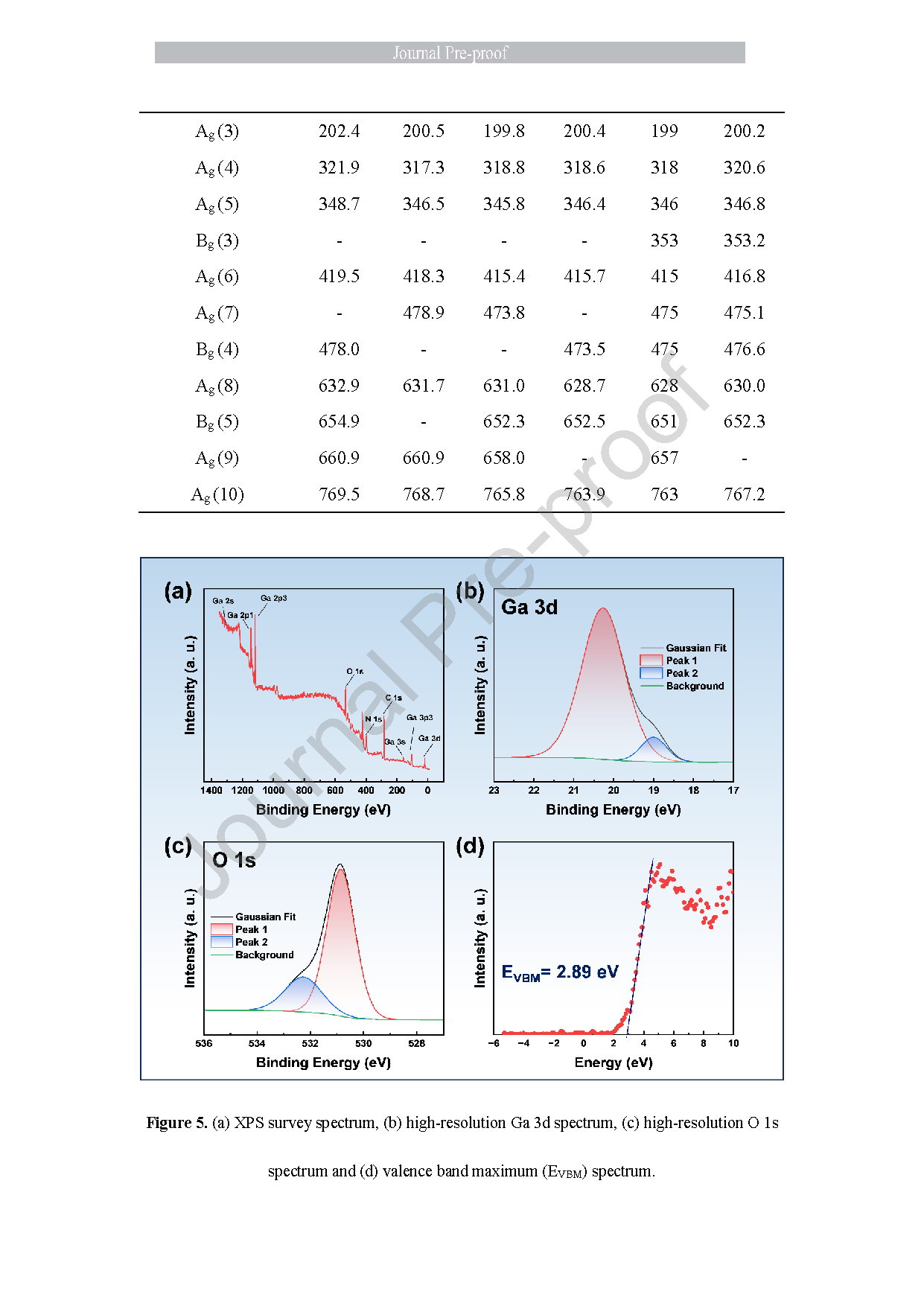
In summary, the feasibility of using a 4° miscut (100) β-Ga2O3 crystal grown by the EFG method for homoepitaxial substrates has been verified. The process successfully suppressed shoulder expansion and twin defects. The resulting CMP substrate exhibited high quality, as confirmed by a narrow X-ray rocking curve with a FWHM of 73.89 arcsec. Optical measurements showed a sharp rise in transmittance from 274 nm, stabilizing near 80% and yielding an optical bandgap of 4.52 eV. Raman spectra closely matched the (100) plane, showing all characteristic peaks except Ag(1), Ag(7) and Bg(3). XPS analysis confirmed trace Ga⁺ and oxygen vacancies, an estimated valence band maximum of 2.89 eV, and a derived surface barrier of 1.63 eV. Wet etching produced elliptical pits that distinct from the (100) plane. Observation of the (010) cross-section revealed nanopipes near the surface, suggesting solid-liquid interface instability and bubble entrapment requiring further optimization. Overall, the directly grown 4° miscut (100) face demonstrates good quality and optoelectronic properties. This single-step approach avoids the material waste associated with the conventional two-step process of first growing a (100) crystal and then preparing a miscut substrate, thereby improving production efficiency.
Project Support
This work was financially supported by the Shenzhen Fundamental Research Program (Grant No. GJHZ20220913142605011), the National Key Research and Development Program of China (2024YFA1208800), the National Natural Science Foundation of China (NSFC) (Grant Number: 52572176, U23A20358), the Natural Science Foundation of Shandong Province (Grant Nos. ZR2023ZD05 and 2022TSGC2120).
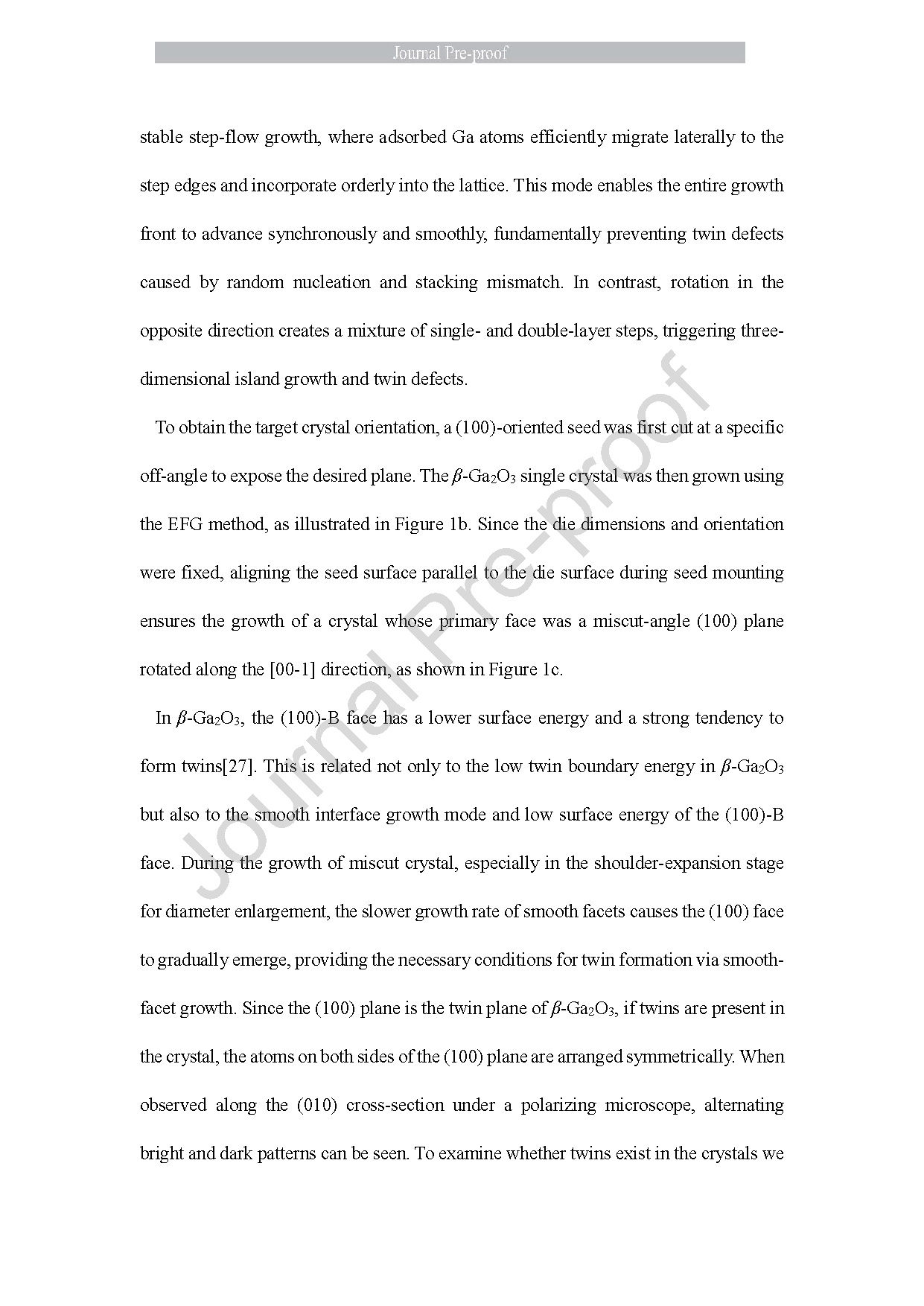
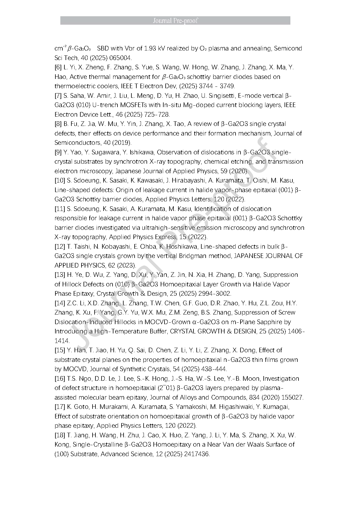
Figure. 1 (a) Schematic diagram illustrating the positional relationship between the (100) plane and the target miscut plane, (b) diagram of the EFG method, (c) as-grown beita-gallium oxide single crystal with the a miscut-angle of (100) plane as its main surface and (d) twins observed in the crystal cross-section under a polarized light scope.
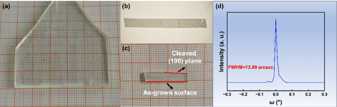
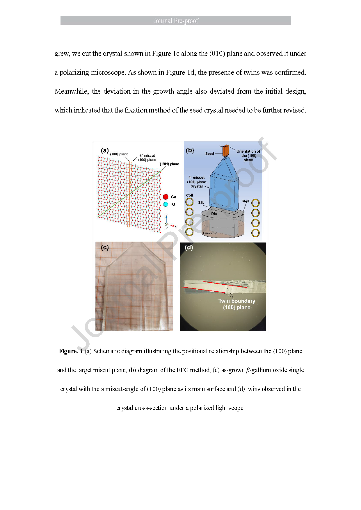
Figure 2. (a) Crystal with the 4° miscut (100) plane as the primary surface grown after modifying the growth process, (b) Observation of the (010) cross-section of the crystal under a polarized light scope, (c) Positional relationship between the growth surface and the (100) cleavage plane. and (d) HRXRD rocking curve.
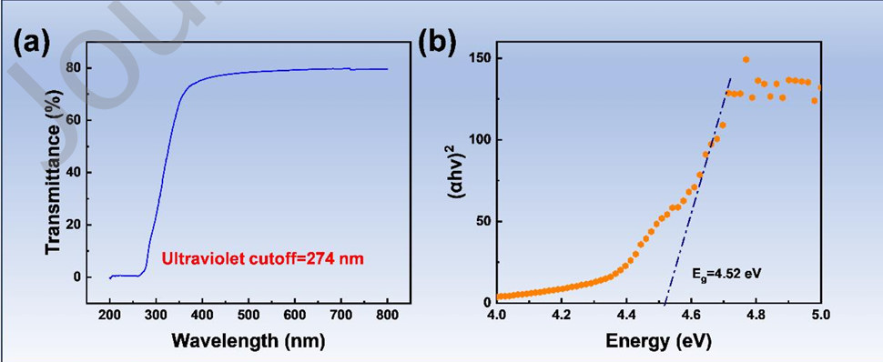
Figure 3. (a) UV-vis transmittance spectrum of the β-Ga2O3 4° miscut (100) plane and (b) bandgap of the β-Ga2O3 4° miscut (100) plane.
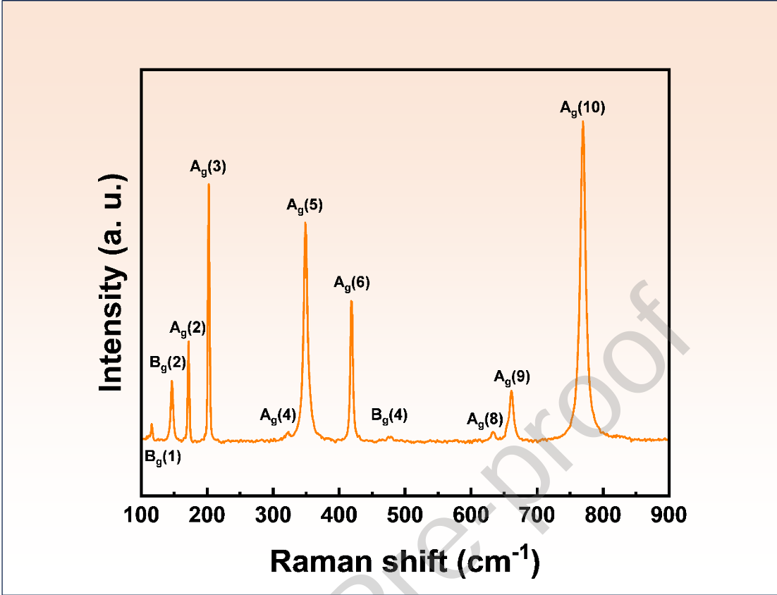
Figure 4. Raman spectrum of the 4° miscut (100) plane.
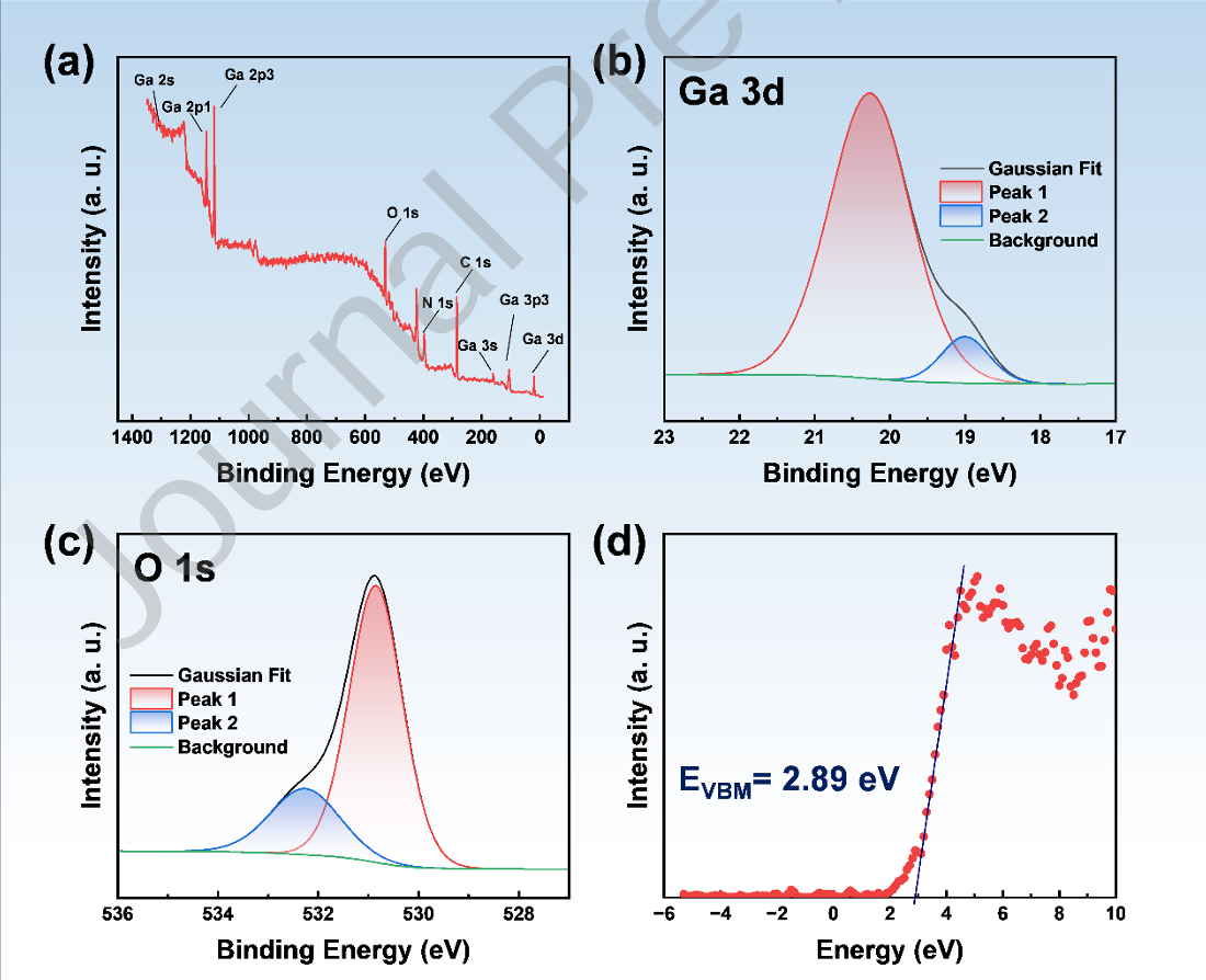
Figure 5. (a) XPS survey spectrum, (b) high-resolution Ga 3d spectrum, (c) high-resolution O 1s spectrum and (d) valence band maximum (EVBM) spectrum.
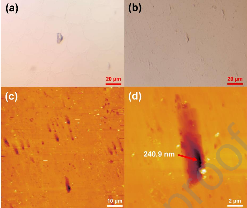
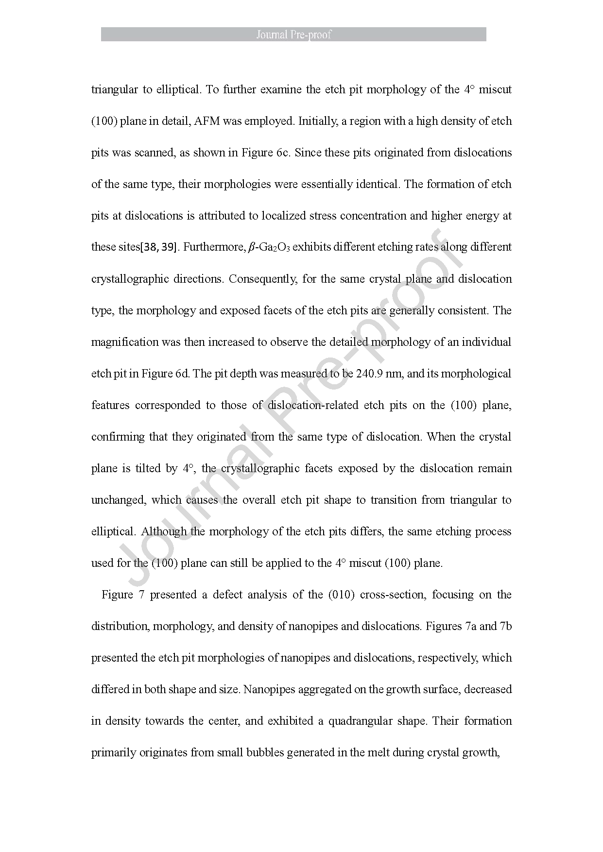
Figure 6. (a) Etch pit morphology of the (100) plane observed by optical microscopy, (b) etch pit morphology of the 4° miscut (100) plane observed by optical microscopy, (c) etch pit distribution of the 4° miscut (100) plane observed by atomic force microscopy, and (d) magnified view of an etch pit observed by atomic force microscopy.
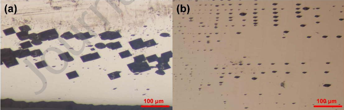
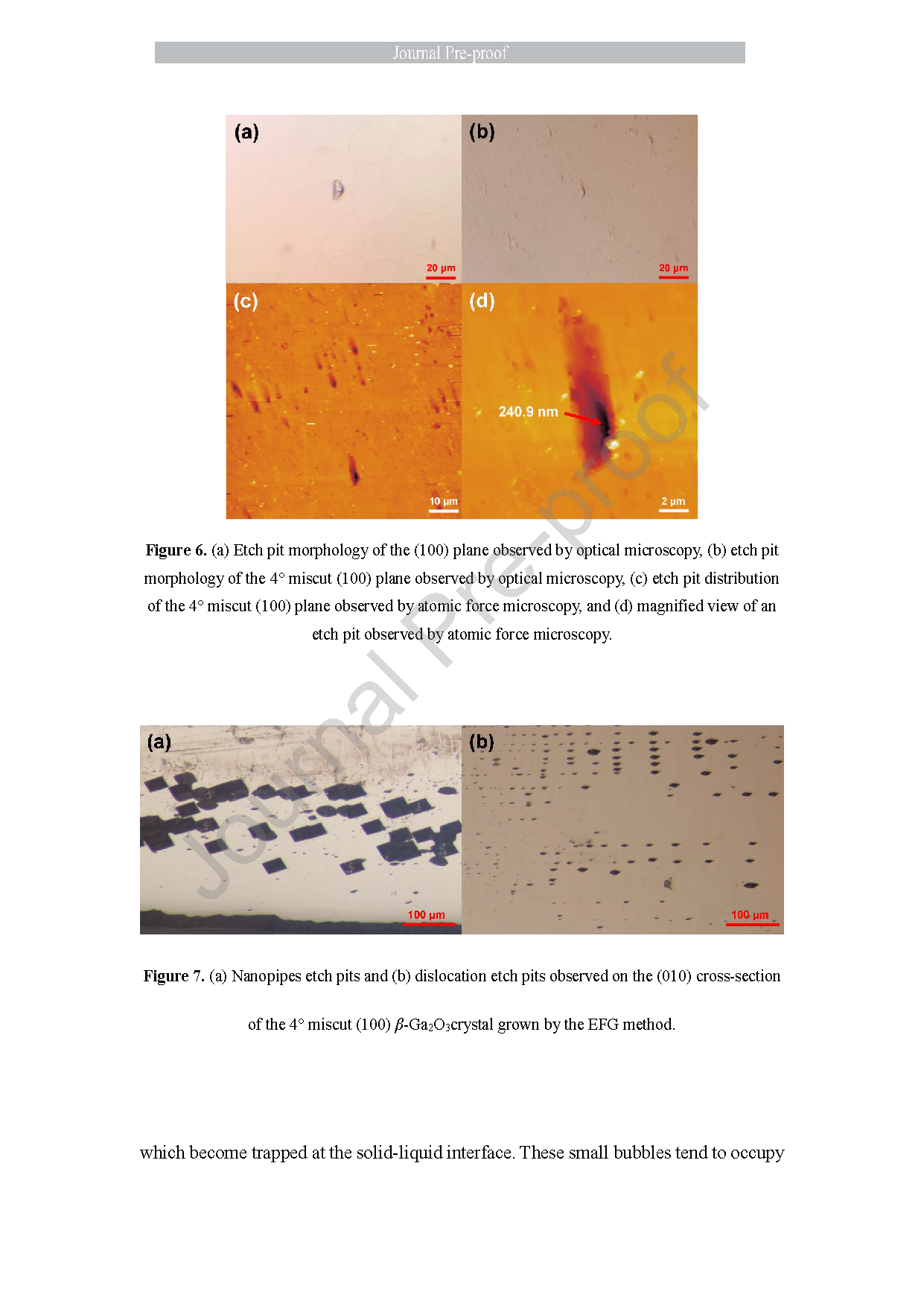
Figure 7. (a) Nanopipes etch pits and (b) dislocation etch pits observed on the (010) cross-section of the 4° miscut (100) β-Ga2O3 crystal grown by the EFG method.
DOI:
doi.org/10.1016/j.jallcom.2026.188151