Paper Sharing
【Member Papers】Liquid-metal-printed buffer layer enabling offcut-tolerant MOCVD heteroepitaxy of β-Ga₂O₃ on sapphire
日期:2026-05-06阅读:174
Researchers from Chaozhou Branch of Chemistry and Chemical Engineering Guangdong Laboratory and JFS Laboratory have published a dissertation titled " Liquid-metal printed buffer layer enabling offcut-tolerant MOCVD heteroepitaxy of β-Ga2O3 on sapphire " in Journal of Alloys and Compounds.
Background
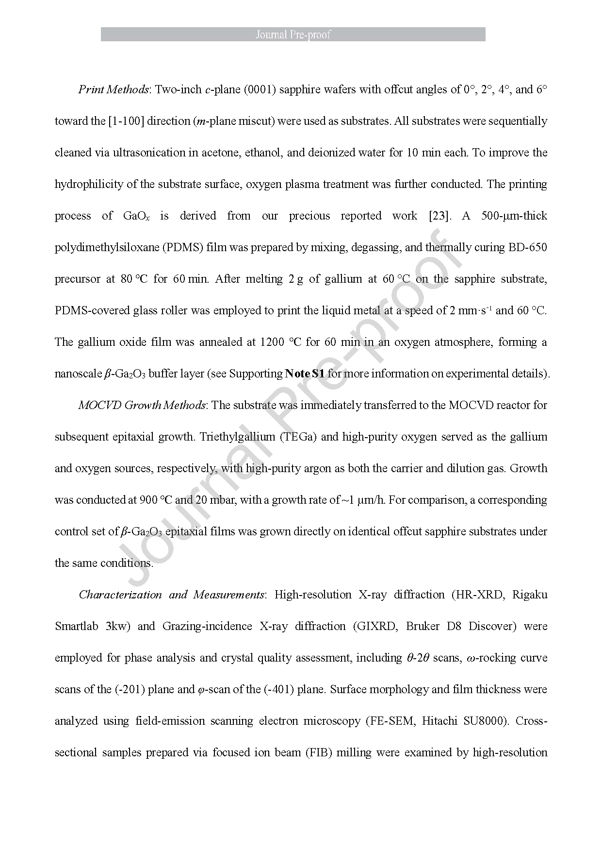
Monoclinic gallium oxide (β-Ga2O3) has garnered significant attention as an ultra-wide-bandgap semiconductor for next-generation power electronics and solar-blind ultraviolet optoelectronics. The heteroepitaxial growth of β-Ga2O3 via metalorganic chemical vapor deposition (MOCVD) represents critical fabrication strategy for producing high-quality films with well-defined band structures and electrical properties. Neverthless, achieving uniform and reproducible epitaxy on foreign substrates presents fundamentally challenging. This difficulty arises from the highly sensitive of heteroepitaxy to the initial interfacial conditions established during the earliest stages of nucleation. Specifically, substrate surface geometry defined by surface atomic steps and local bonding environments, collectively dictate growth mode selection and defect formation. In of the context of β-Ga2O3 heteroepitaxy, this sensitivity is further exacerbated by variations in substrate offcut angles, which influence step-flow dynamics. Consequently, these variarions lead to inconsistent nucleation behavior, variable crystalline quality, and limited process reproducibility.
Abstract
Heteroepitaxial growth of β-Ga2O3 is typically constrained by a pronounced sensitivity to substrate offcut angles, which dictates surface step dynamics and nucleation behavior, thereby limiting film uniformity and reproducibility. Herein, we report an interface-engineering strategy utilizing a liquid-metal-printed Ga2O3 buffer layer that employs a structurally reconfigurable precursor. Upon thermal oxidation and controlled crystallization, this ultrathin buffer effectively reconstructs the interfacial conditions and governs the early stages of epitaxy, thereby providing a quasi-homoepitaxial template for subsequent metalorganic chemical vapor deposition (MOCVD) growth of β-Ga2O3 films. Significantly, the buffer layer enables the growth of β-Ga2O3 films with systematically improved crystalline coherence, reduced surface roughness, and enhanced morphological uniformity across sapphire substrates with offcut angles ranging from 0° to 6°. This interface-engineering effect significantly mitigates the constraint imposed by substrate geometry, resulting in markedly improved process tolerance. This work underscores the effectiveness of liquid-metal-printed buffer layers as reconfigurable interface precursors for regulating epitaxial growth sensitivity, offering a low-cost and scalable method to alleviate substrate geometry constraints. It establishes a robust paradigm for high quality β-Ga2O3 heteroepitaxy on sapphire, contributing to advancements in electronic and optoelectronic material platforms.
Conclusion
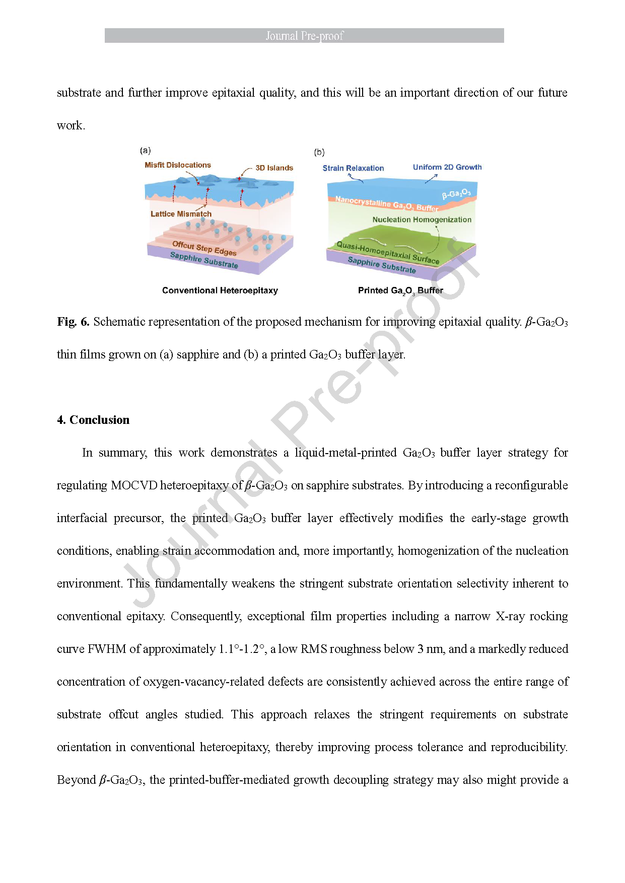
In summary, this work demonstrates a liquid-metal-printed Ga2O3 buffer layer strategy for regulating MOCVD heteroepitaxy of β-Ga2O3 on sapphire substrates. By introducing a reconfigurable interfacial precursor, the printed Ga2O3 buffer layer effectively modifies the early-stage growth conditions, enabling strain accommodation and, more importantly, homogenization of the nucleation environment. This fundamentally weakens the stringent substrate orientation selectivity inherent to conventional epitaxy. Consequently, exceptional film properties including a narrow X-ray rocking curve FWHM of approximately 1.1°-1.2°, a low RMS roughness below 3 nm, and a markedly reduced concentration of oxygen-vacancy-related defects are consistently achieved across the entire range of substrate offcut angles studied. This approach relaxes the stringent requirements on substrate orientation in conventional heteroepitaxy, thereby improving process tolerance and reproducibility. Beyond β-Ga2O3, the printed-buffer-mediated growth decoupling strategy may also might provide a versatile interface-engineering route for achieving robust heteroepitaxy of wide-bandgap semiconductors on non-native substrates.
Project Support
This work was supported by the Chaozhou City Ceramics Industry Talent Revitalization Plan Project (GXYJ001) and the National Natural Science Foundation of China (No. 52472072 & No. 52502075). The authors would like to acknowledge the support of Major Program (JD) of Hubei Province (2023BAA009), and JFS Laboratory.
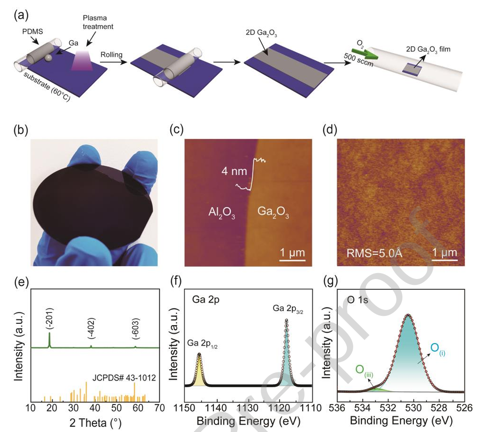
Fig. 1. Printing fabrication and characterization of the β-Ga2O3 buffer layer. (a) Schematic representation of the fabrication process for the β-Ga2O3 buffer layer. (b) Optical image of two-inch uniform GaOx film printed on silicon. (c) AFM image and (d) RMS roughness of β-Ga2O3 buffer layer after annealing. (e) GIXRD pattern of β-Ga2O3 buffer layer. XPS pattern of Ga 2p (f) and O 1s (g) for the β-Ga2O3 buffer layer.
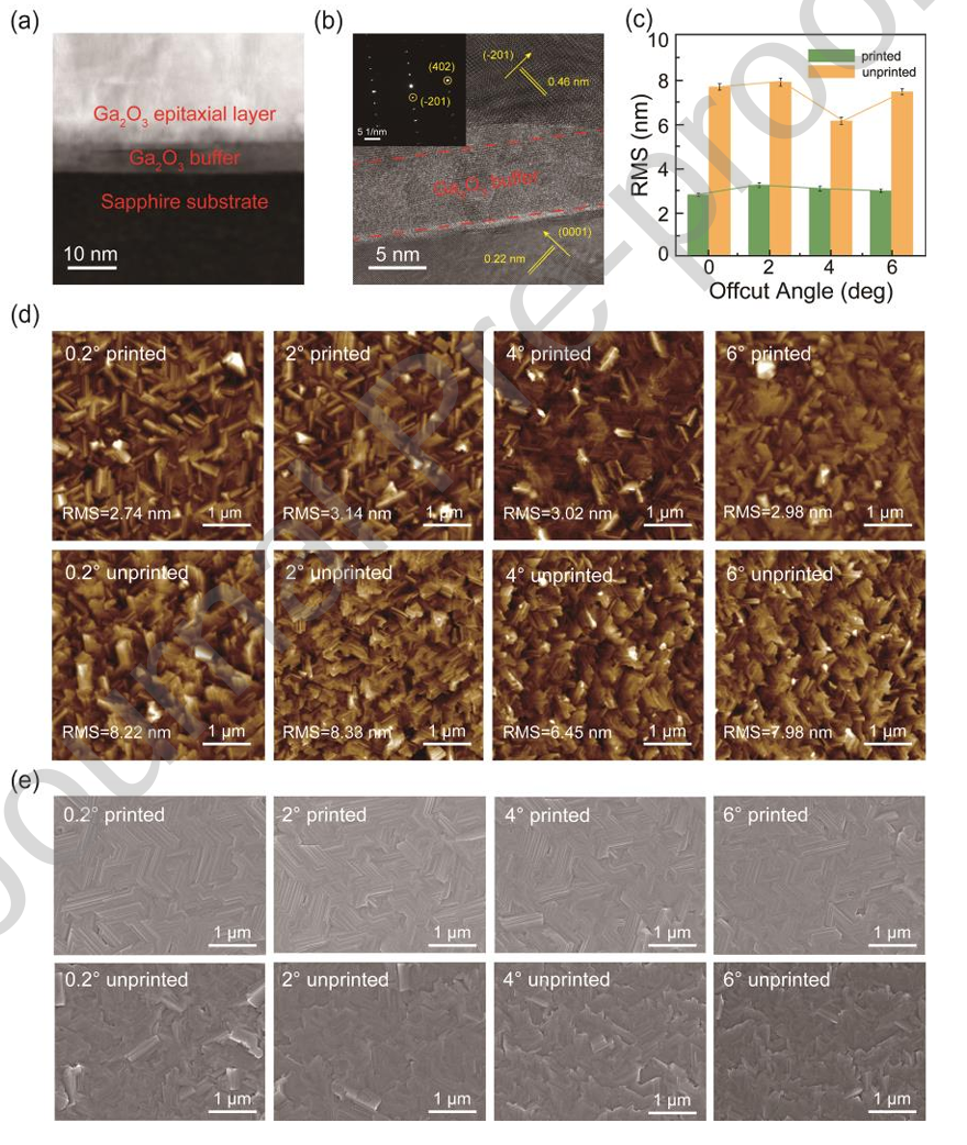
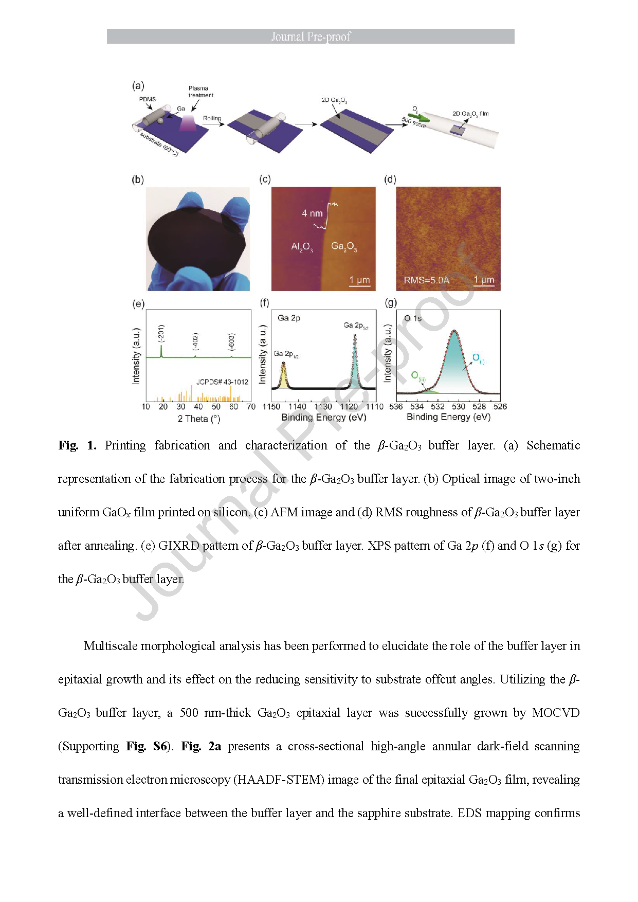
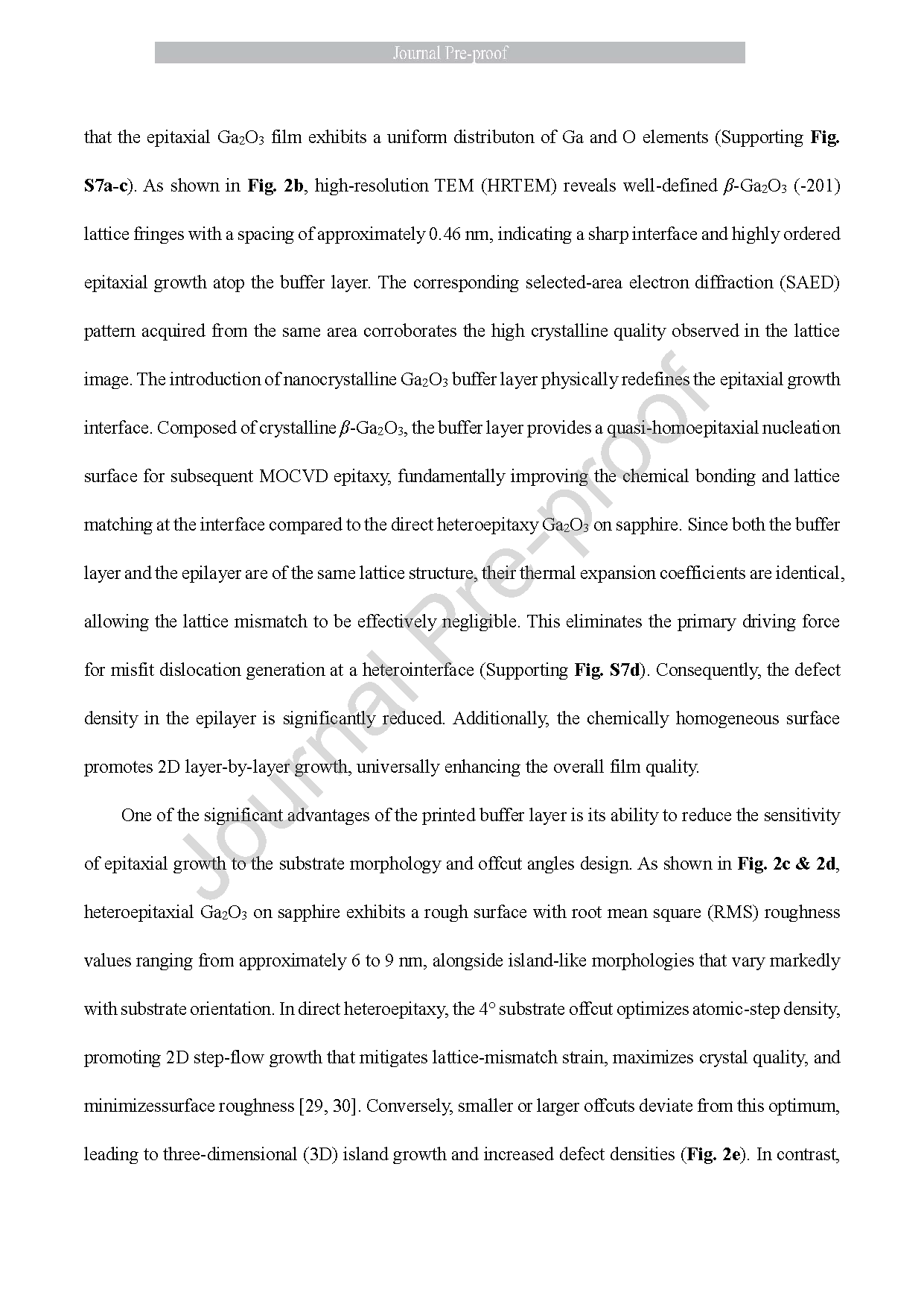
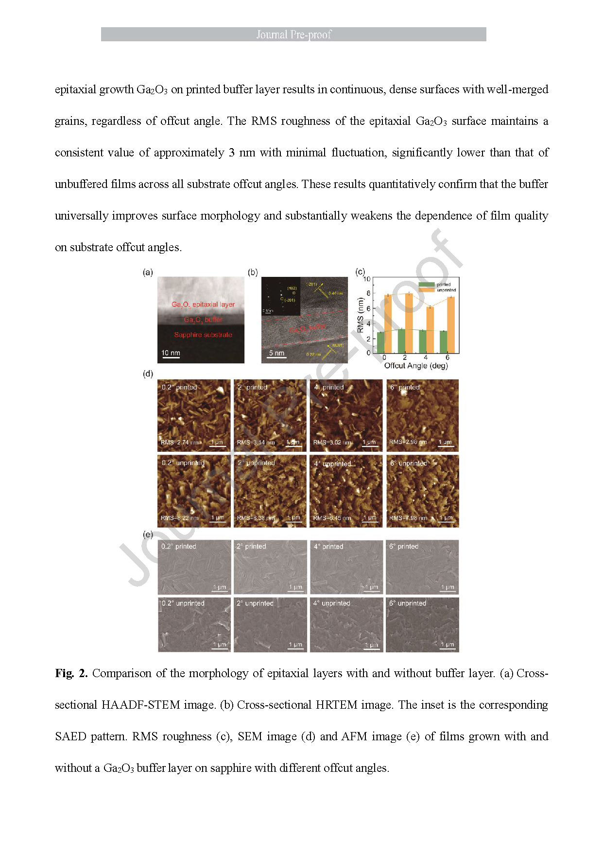
Fig. 2. Comparison of the morphology of epitaxial layers with and without buffer layer. (a) Cross sectional HAADF-STEM image. (b) Cross-sectional HRTEM image. The inset is the corresponding SAED pattern. RMS roughness (c), SEM image (d) and AFM image (e) of films grown with and without a Ga2O3 buffer layer on sapphire with different offcut angles.
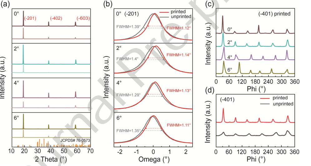
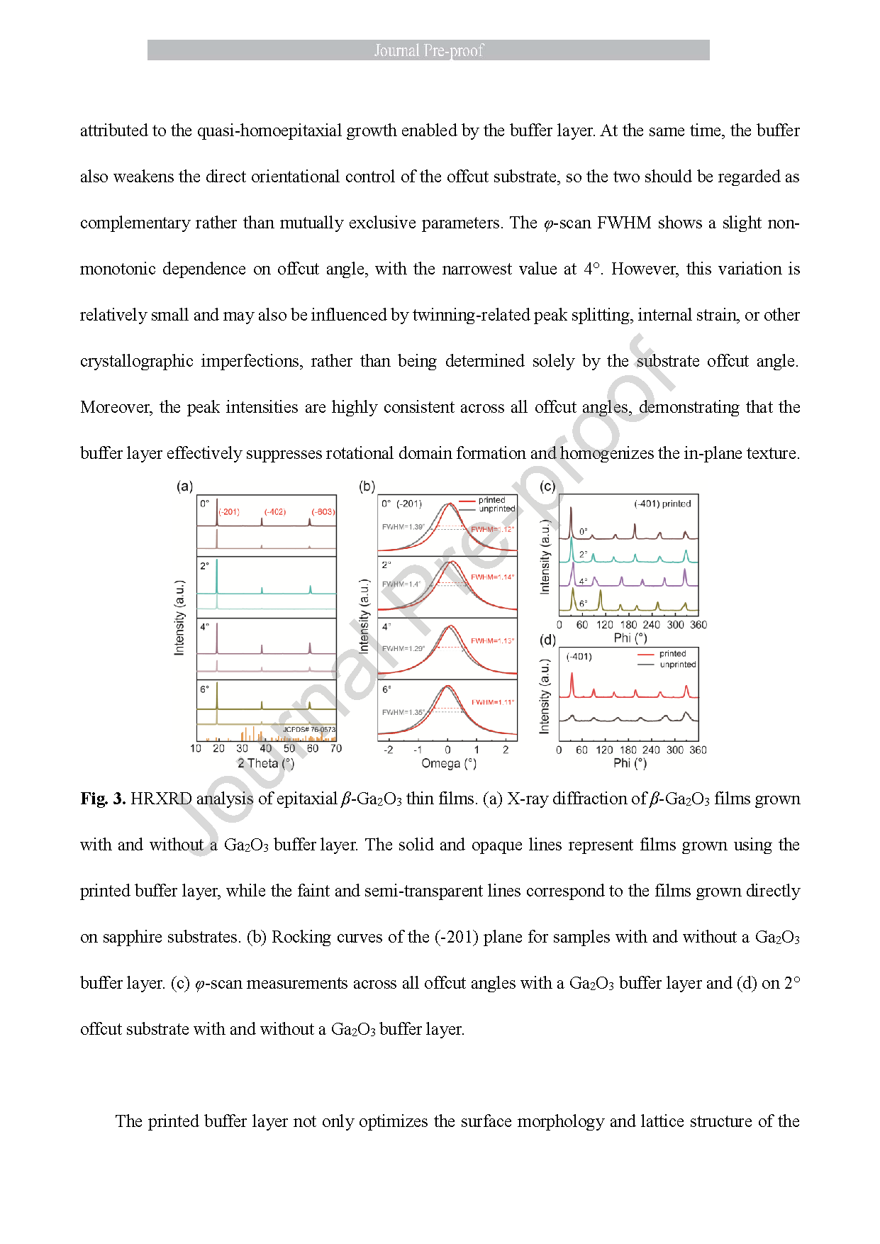
Fig. 3. HRXRD analysis of epitaxial β-Ga2O3 thin films. (a) X-ray diffraction of β-Ga2O3 films grown with and without a Ga2O3 buffer layer. The solid and opaque lines represent films grown using the printed buffer layer, while the faint and semi-transparent lines correspond to the films grown directly on sapphire substrates. (b) Rocking curves of the (-201) plane for samples with and without a Ga2O3 buffer layer. (c) φ-scan measurements across all offcut angles with a Ga2O3 buffer layer and (d) on 2° offcut substrate with and without a Ga2O3 buffer layer.
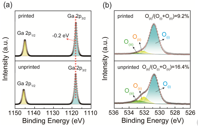
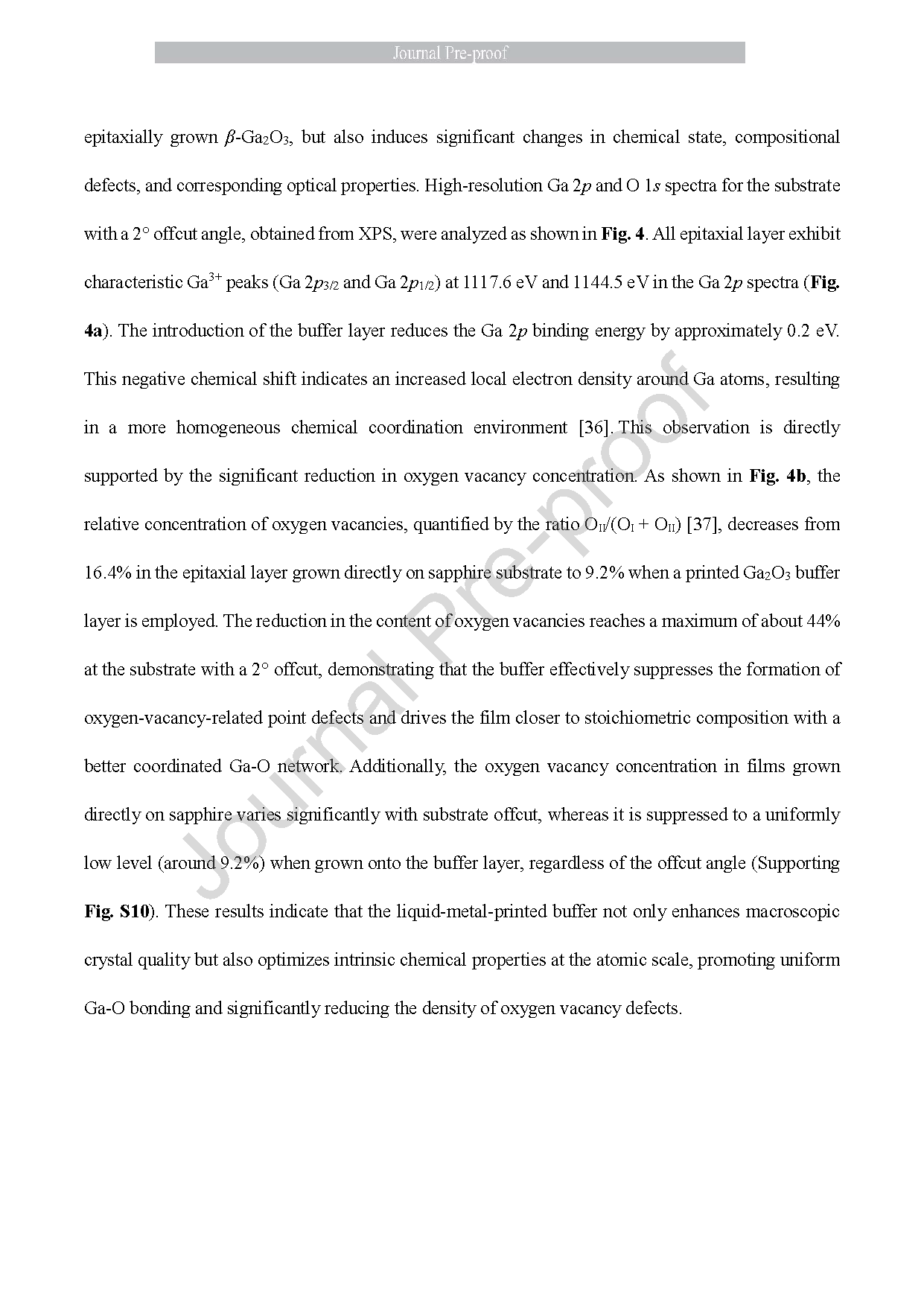
Fig. 4. Variation of the chemical state of epitaxially grown Ga2O3 layer. XPS pattern of (a) Ga 2p and (b) O 1s for β-Ga2O3 films grown on sapphire substrates with 2° offcut angle, both with and without a Ga2O3 buffer layer.
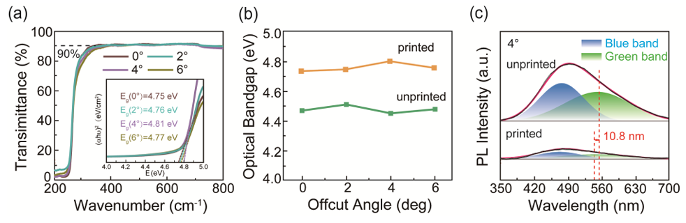
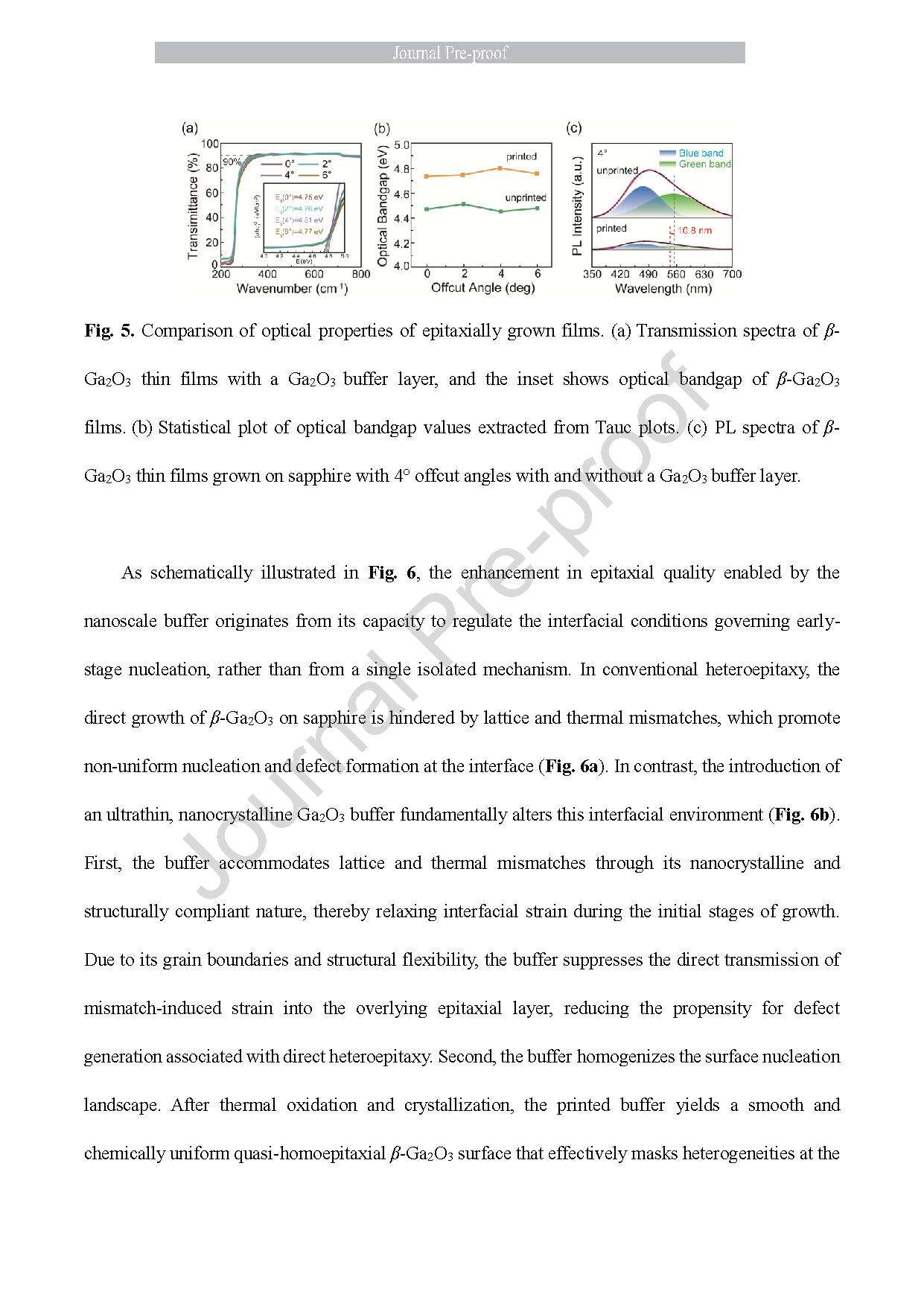
Fig. 5. Comparison of optical properties of epitaxially grown films. (a) Transmission spectra of β Ga2O3 thin films with a Ga2O3 buffer layer, and the inset shows optical bandgap of β-Ga2O3 films. (b) Statistical plot of optical bandgap values extracted from Tauc plots. (c) PL spectra of β Ga2O3 thin films grown on sapphire with 4° offcut angles with and without a Ga2O3 buffer layer.
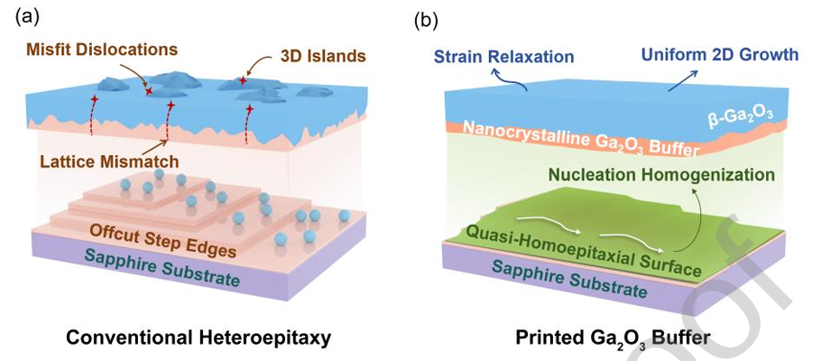
Fig. 6. Schematic representation of the proposed mechanism for improving epitaxial quality. β-Ga2O3 thin films grown on (a) sapphire and (b) a printed Ga2O3 buffer layer.
DOI:
doi.org/10.1016/j.jallcom.2026.188281