Paper Sharing
【Member Papers】High-Performance Self-Driven Ultraviolet Photodetector Based on Sol–Gel Derived NiO/Sn:Ga₂O₃ p–n Junction
日期:2026-05-07阅读:14
Researchers from Hubei University and Wuhan Textile University have published a paper titled “High-Performance Self-Driven Ultraviolet Photodetector Based on Sol–Gel Derived NiO/Sn:Ga₂O₃ p–n Junction” in ACS Applied Electronic Materials.
Background
Solar-blind ultraviolet photodetectors have important application value in fire monitoring, corona detection, military early warning and other fields. Ga₂O₃ has become an ideal candidate material due to its ultra-wide bandgap and high stability. Traditional high-performance Ga₂O₃ devices mostly rely on complex processes such as vacuum deposition and vapor phase epitaxy, which have high cost and difficulty in large-scale production. In addition, intrinsic Ga₂O₃ has low carrier concentration and weak built-in electric field of p-n junction, resulting in that the responsivity and detectivity of self-driven devices are difficult to meet practical requirements. At present, there is still a lack of research on high-performance self-driven ultraviolet detection using low-cost sol-gel process and regulating carriers and heterojunction built-in electric field through Sn doping, and the contradiction between device performance and preparation cost has not been effectively solved.
Abstract
Ga₂O₃-based self-driven solar-blind ultraviolet (SBUV) photodetectors have attracted considerable attention for their promising applications in military, civil, and industrial fields. However, conventional manufacturing methods for high-performance Ga₂O₃ photodetectors typically require complex processes and high costs, thereby severely constraining their practical applications. In this work, we demonstrate a high-performance NiO/Sn:Ga₂O₃ p−n junction SBUV photodetector fabricated by a low-cost sol−gel method. The device exhibits an excellent photocurrent response under zero bias, with a responsivity (R) of 47.89 mA/W and a detectivity (D*) of 4.60 ×10¹¹ Jones at 240 nm. These performance parameters are remarkably higher than those of the Ga₂O₃ device (R=7.91 mA/W, D*=0.61 ×10¹¹ Jones) and the NiO/Ga₂O₃ device (R=19.36 mA/W, D*=2.61 ×10¹¹ Jones). Under weak light illumination (P₂₅₅ nm=0.53 μW/cm²), the R and D* of the NiO/Sn:Ga₂O₃ SBUV photodetector reach 150.6 mA/W and 1.33 ×10¹² Jones, respectively, which are superior to most reported NiO/Ga₂O₃-based photodetectors. The ultrahigh performance can be attributed to the enhanced built-in electric field at the NiO/Sn:Ga₂O₃ p-n junction interface and the improved electrical transport properties of the Sn:Ga₂O₃ layer. This study provides a feasible route toward the development of low-cost, high-performance Ga₂O₃-based self-driven UV photodetectors.
Highlights
Fabricated high-performance self-driven NiO/Sn:Ga₂O₃ p-n junction SBUV photodetectors via a low-cost sol−gel method.
Achieved a responsivity of 47.89 mA/W and a detectivity of 4.60 ×10¹¹ Jones at 240 nm under zero bias.
Realized ultrahigh performance of 150.6 mA/W and 1.33 ×10¹² Jones under weak light illumination.
Enhanced built-in electric field at the NiO/Sn:Ga₂O₃ interface by Sn doping of Ga₂O₃.
Provided a low-cost and feasible strategy for high-performance Ga₂O₃-based self-driven photodetectors.
Conclusion
In summary, a high-performance self-driven NiO/Sn:Ga₂O₃ p-n junction UV photodetector was fabricated using a low-cost sol−gel method. At zero bias, the device achieved a responsivity of 47.89 mA/W and a detectivity of 4.60 ×10¹¹ Jones at 240 nm, along with a short response time (τᵣ/τd=0.251 s/0.245 s). Under weak light illumination (0.53 μW/cm² at 255 nm), the responsivity and detectivity were further enhanced to 150.6 mA/W and 1.33 ×10¹² Jones, respectively. These figures of merit (R, D*, τᵣ/τd) markedly surpass those of most reported state-of-the-art NiO/Ga₂O₃-based photodetectors. Benefiting from a simple, low-cost, and scalable fabrication process, this work provides a practical and scalable strategy for developing high-performance, self-driven UV photodetectors.
Project Support
This work was supported by the National Natural Science Foundation of China (Grant Nos. 62274057, 52202132, and 11975093), the Program for Science and Technology Innovation Team in Colleges of Hubei Province (Grant No. T201901), the Hubei International Science and Technology Cooperation Project (Grant No. 2025EHA006), and the Wuhan Municipal Bureau of Science and Technology Innovation (Grant Nos. 2024040801020306 and 2025011202030396).
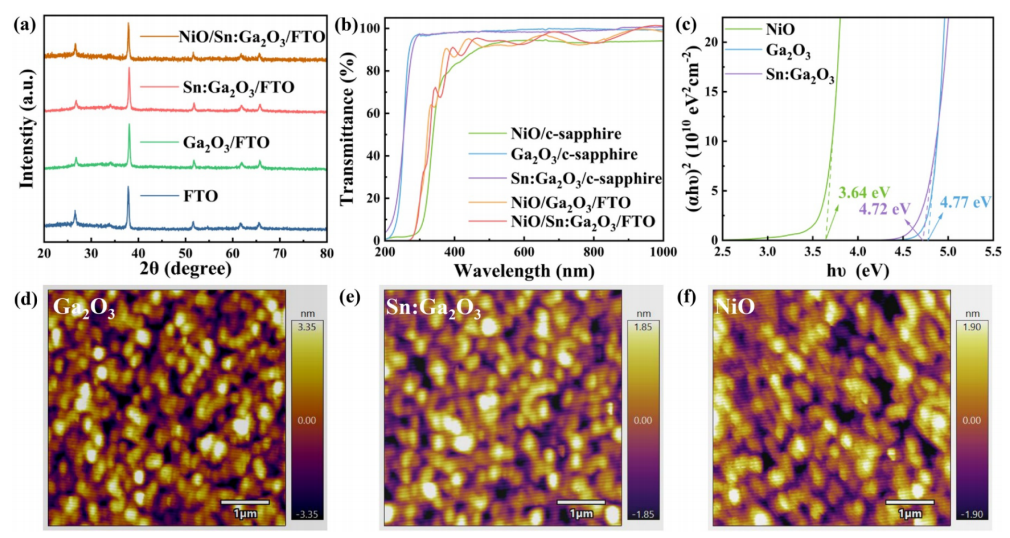
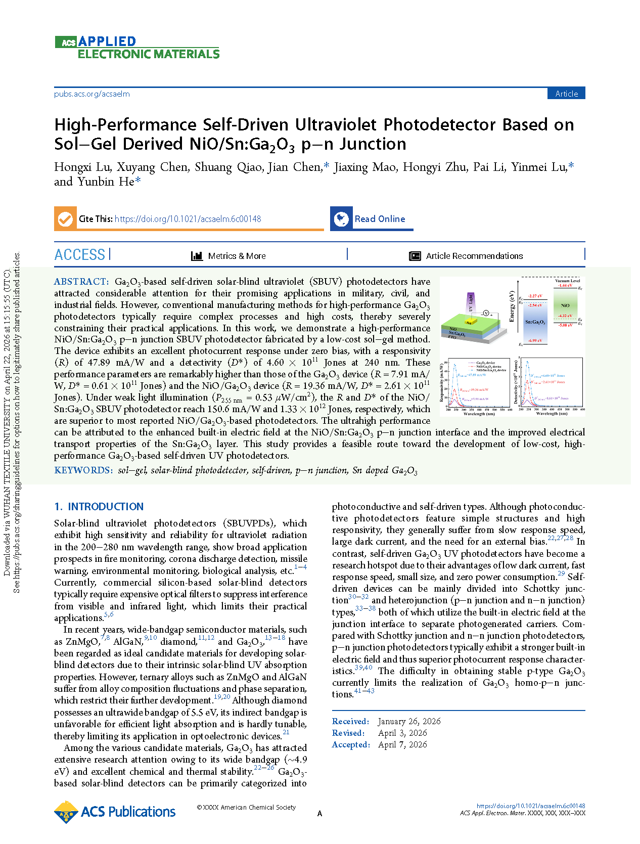
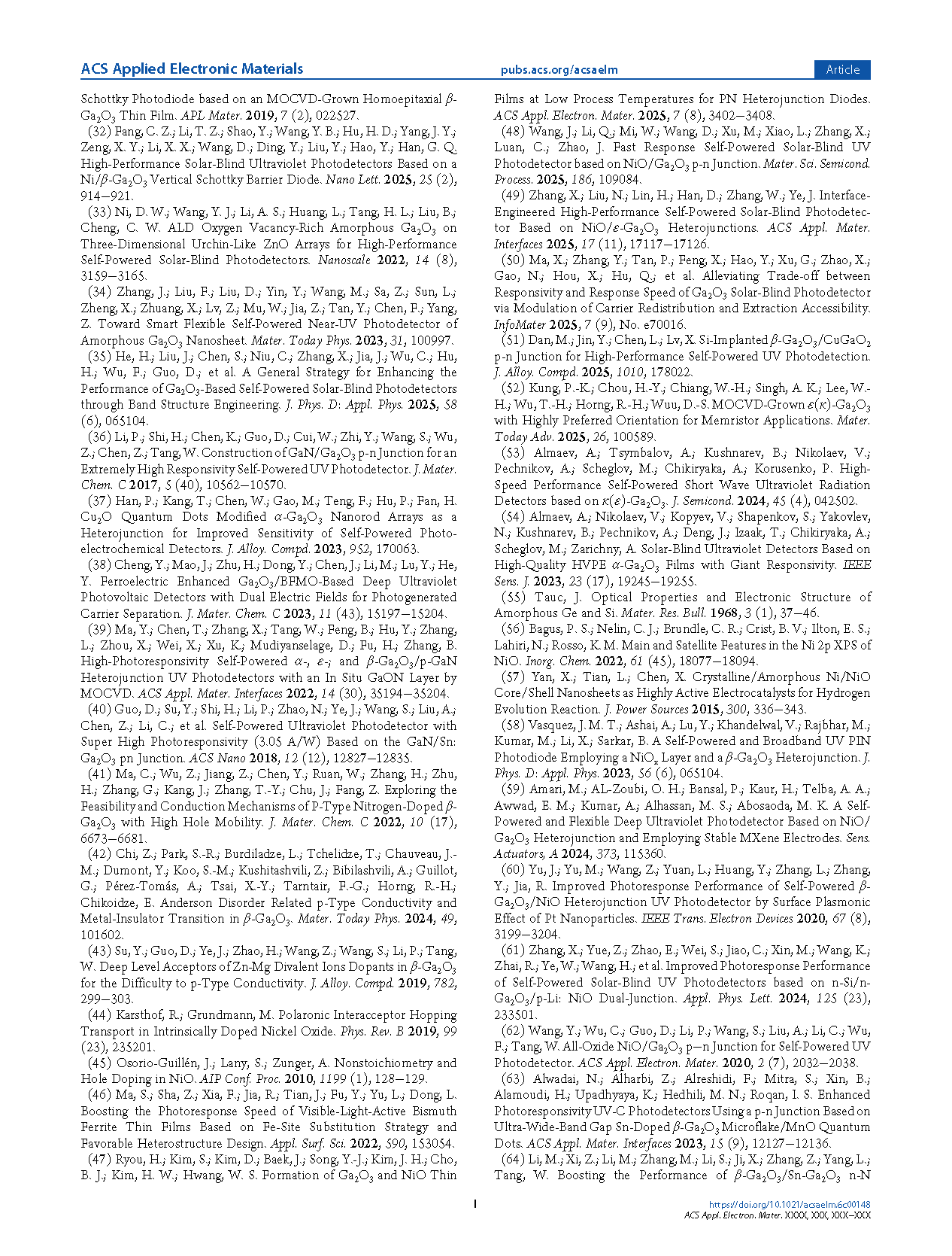
Figure 1. (a) XRD patterns of the FTO glass substrate, Ga₂O₃/FTO, Sn:Ga₂O₃/FTO, and NiO/Sn:Ga₂O₃/FTO films. (b) Optical transmission spectra of the NiO, Ga₂O₃, Sn:Ga₂O₃, NiO/Ga₂O₃, and NiO/Sn:Ga₂O₃ heterojunction film. (c) Plots of (αhν)²-hν of the NiO, Ga₂O₃, and Sn:Ga₂O₃ films. (d−f) AFM surface images of the Ga₂O₃/FTO, Sn:Ga₂O₃/FTO, and NiO/Sn:Ga₂O₃/FTO films.
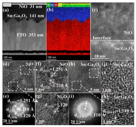
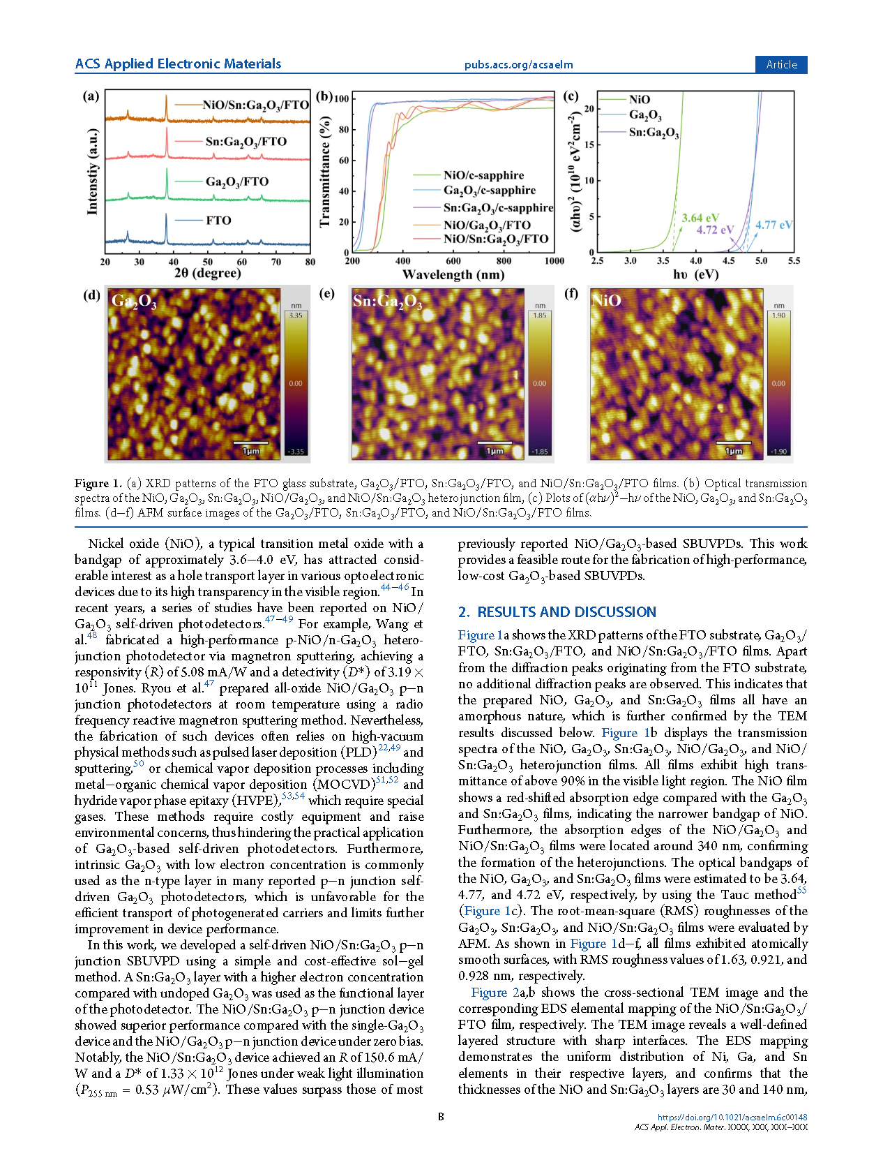
Figure 2. (a) Cross-sectional TEM image and (b) EDS elemental mapping of the NiO/Sn:Ga₂O₃/FTO multilayer film. (c) HRTEM image at the NiO/Sn:Ga₂O₃ interface. HRTEM images and corresponding FFT images of (d,e) NiO and (h,i) Sn:Ga₂O₃ thin films, and (f,g) and (j,k) are enlarged images of the dashed box regions in the HRTEM images of NiO and Sn:Ga₂O₃, respectively.
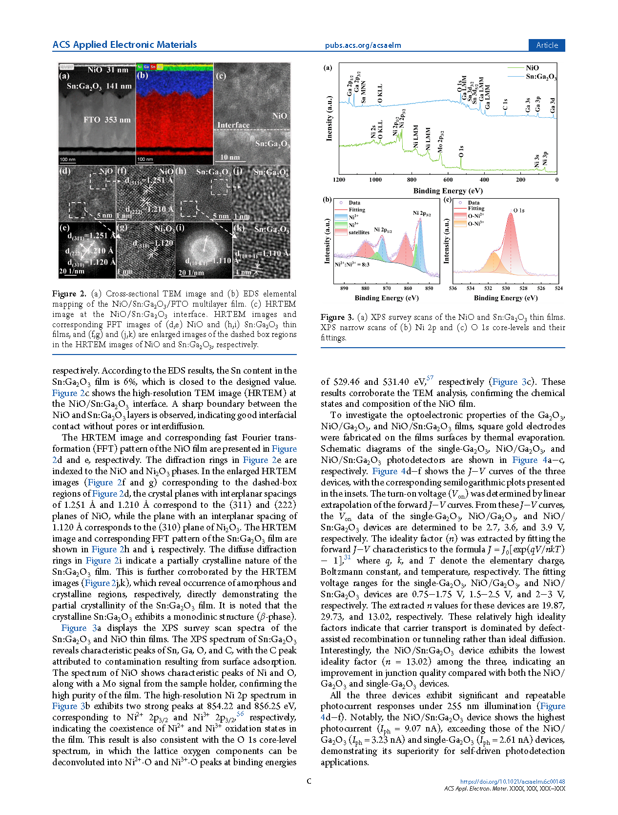
Figure 3. (a) XPS survey scans of the NiO and Sn:Ga₂O₃ thin films. XPS narrow scans of (b) Ni 2p and (c) O 1s core-levels and their fittings.
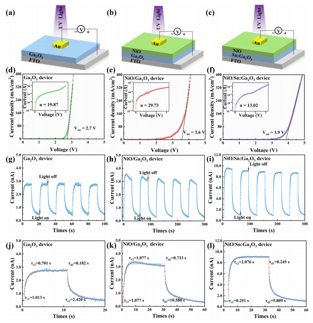
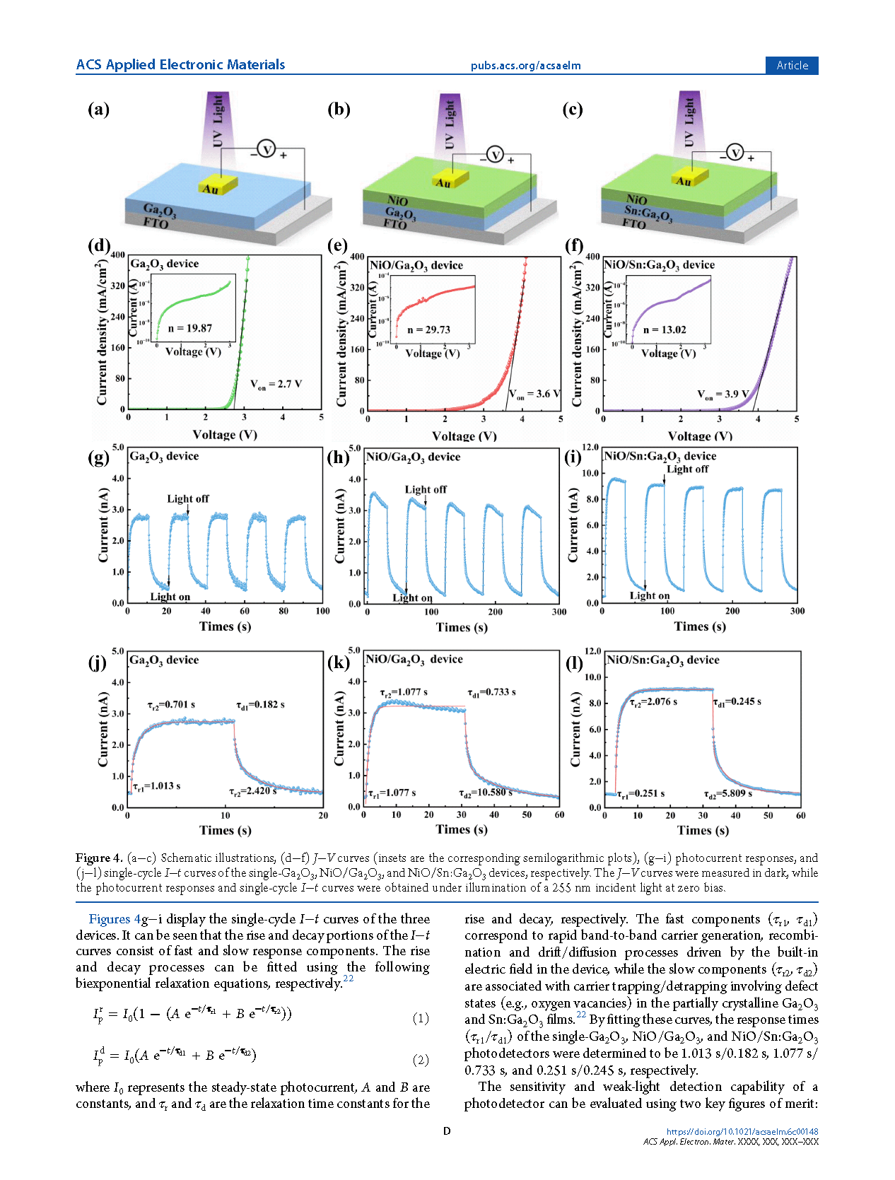
Figure 4. (a−c) Schematic illustrations, (d−f) J−V curves (insets are the corresponding semilogarithmic plots), (g−i) photocurrent responses, and (j−l) single-cycle I−t curves of the single-Ga₂O₃, NiO/Ga₂O₃, and NiO/Sn:Ga₂O₃ devices, respectively. The J−V curves were measured in dark, while the photocurrent responses and single-cycle I−t curves were obtained under illumination of a 255 nm incident light at zero bias.
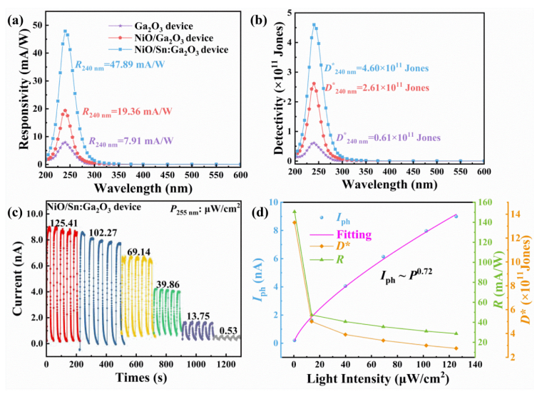
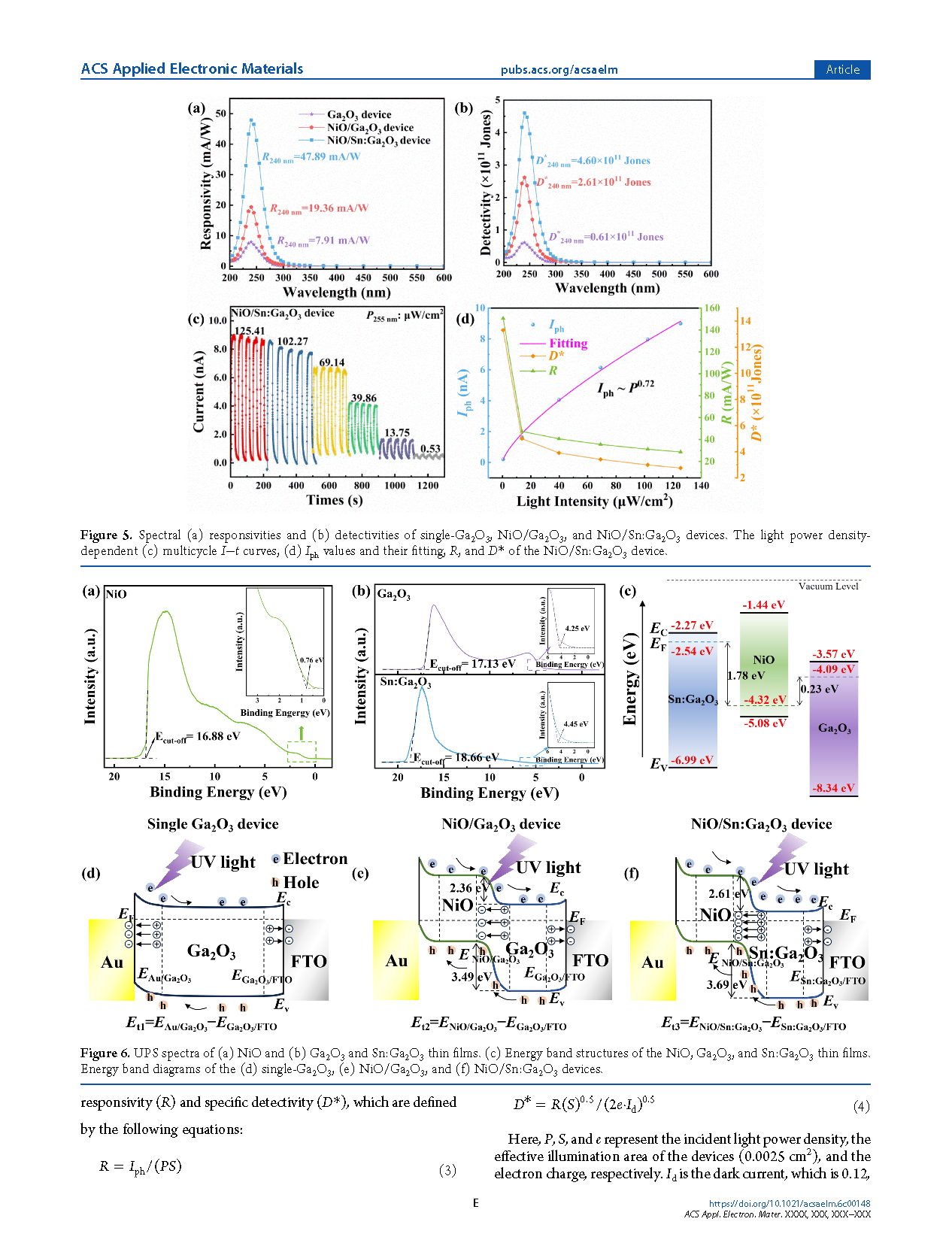
Figure 5. Spectral (a) responsivities and (b) detectivities of single-Ga₂O₃, NiO/Ga₂O₃ and NiO/Sn:Ga₂O₃ devices. The light power density-dependent (c) multicycle I-t curves, (d) Iph values and their fitting, R, and D* of the NiO/Sn:Ga₂O₃ device.
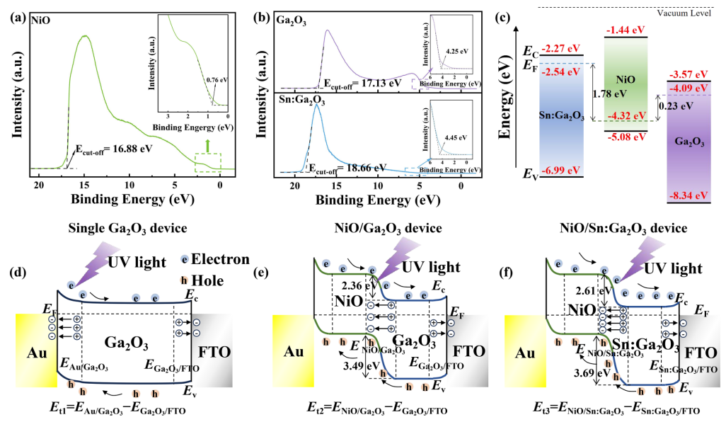
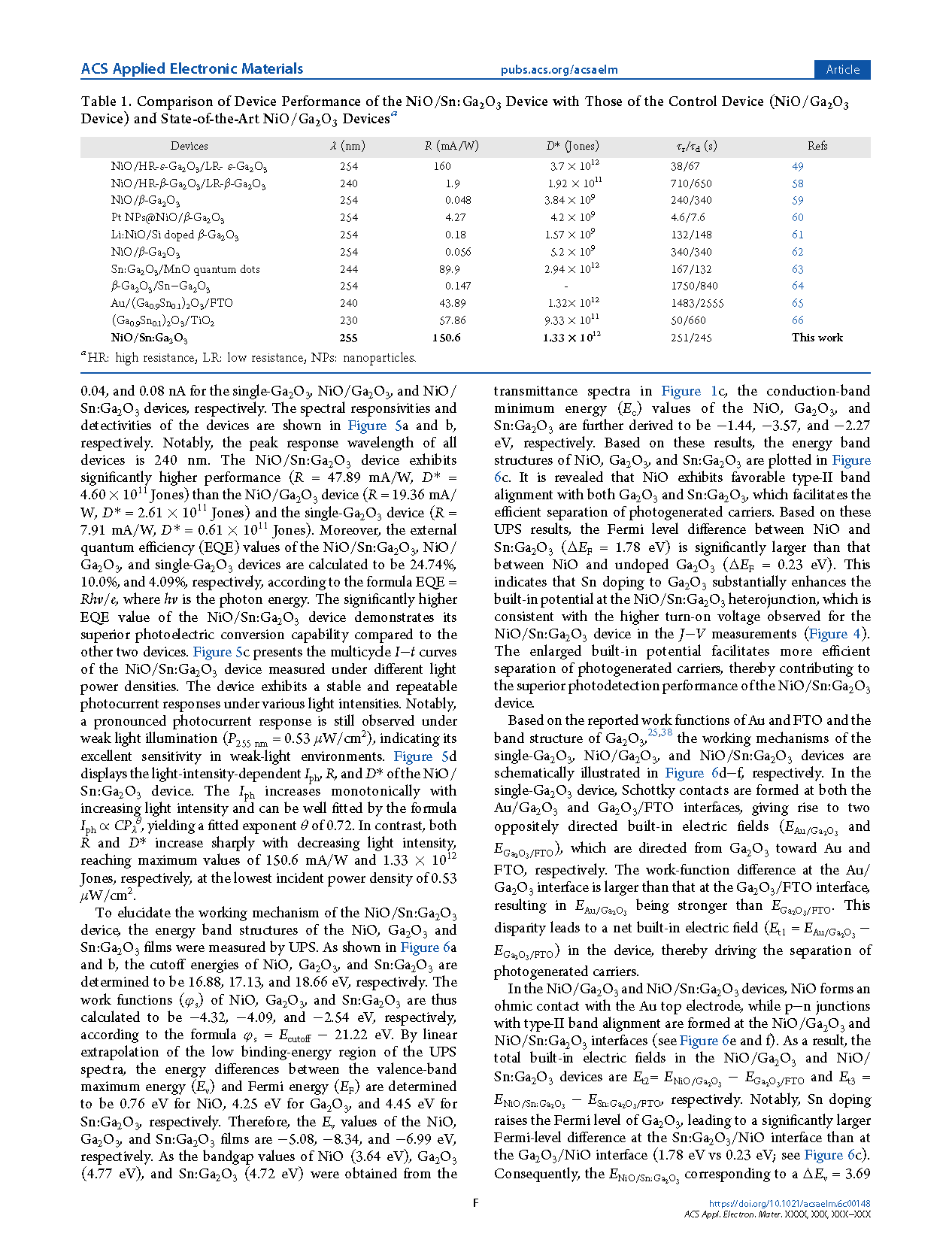
Figure 6. UPS spectra of (a) NiO and (b) Ga₂O₃ and Sn:Ga₂O₃ thin films. (c) Energy band structures of the NiO, Ga₂O₃ and Sn:Ga₂O₃ thin films. Energy band diagrams of the (d) single-Ga₂O₃ (e) NiO/Ga₂O₃, and (f) NiO/Sn:Ga₂O₃ devices.
DOI:
doi.org/10.1021/acsaelm.6c00148