Paper Sharing
【Member Papers】From architectures to device physics: Pathways to integrate lateral, vertical, and heterogeneous schemes in gallium oxide transistors
日期:2026-05-07阅读:16
Researchers from the Nanjing University of Posts and Telecommunications,Inner Mongolia University and the Hong Kong University of Science and Technology have published a dissertation titled "From architectures to device physics: Pathways to integrate lateral, vertical, and heterogeneous schemes in gallium oxide transistors " in Applied Physics Reviews.
Background
With the rapid expansion of strategic emerging industries such as large-scale integrated circuits, artificial intelligence, the Internet of Things, and new energy vehicles, the demand for electronic devices with high frequency, high voltage, and high power characteristics is increasing continuously. The performance of traditional silicon-based semiconductor devices has gradually approached their theoretical limits. Wide-bandgap semiconductors represented by silicon carbide and gallium nitride have gradually realized substitution, but still cannot meet the application requirements of the next generation of extreme working conditions. Ultra-wide bandgap semiconductors with a bandgap greater than 4 eV have become the core research and development direction. Among them, gallium oxide (Ga₂O₃) has become the core candidate material for next-generation ultra-high power and radio frequency devices by virtue of its ultra-wide bandgap of about 4.8 eV, high critical breakdown field strength of 8 MV/cm, achievable efficient n-type doping, and low-cost melt growth advantages, breaking through the doping bottlenecks of materials such as diamond and aluminum nitride. In the past decade, with the breakthroughs in large-size single crystal substrate preparation and epitaxial doping technologies, β-Ga₂O₃ transistors have rapidly evolved from basic research to device verification, and structures such as lateral, vertical, and heterogeneous integration have been continuously iterated. However, bottlenecks such as the p-type doping problem, dynamic on-resistance degradation, and poor heat dissipation performance have not been solved, and there is an urgent need to systematically sort out the technical paths and development directions.
Abstract
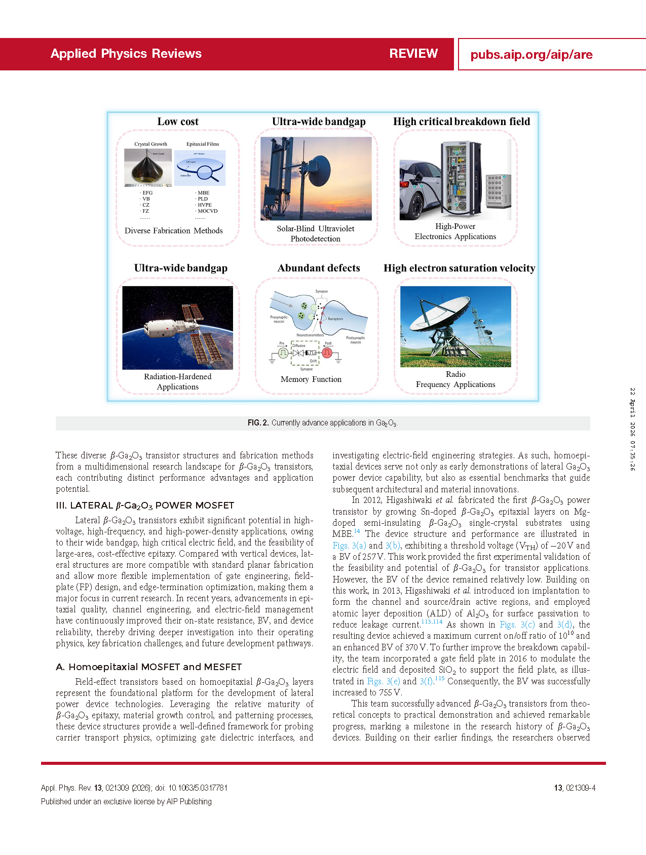
As an emerging ultra-wide bandgap semiconductor, gallium oxide (Ga₂O₃) has attracted considerable research interest since its discovery. It exhibits outstanding material properties and compatibility with low-cost fabrication techniques, making it a highly promising candidate for next-generation ultra-high power and high-frequency applications. Over the past decades, Ga₂O₃-based transistors have undergone rapid development and demonstrated strong potential in various domains. This review systematically summarizes recent progress in the architecture and performance of β-Ga₂O₃ transistors that have garnered significant attention. We approach this review from the perspective of application domains, and within each category, we further discuss device variations in detail based on structural configurations or operating mechanisms. Key structures covered include lateral and vertical β-Ga₂O₃ metal-oxide-semiconductor field-effect transistors for power electronics, radio frequency β-Ga₂O₃ transistors, and β-Ga₂O₃ thin-film transistors for flexible applications. This work aims to provide a comprehensive reference and to inspire future research directions in the field of Ga₂O₃ transistor technologies.
Highlights
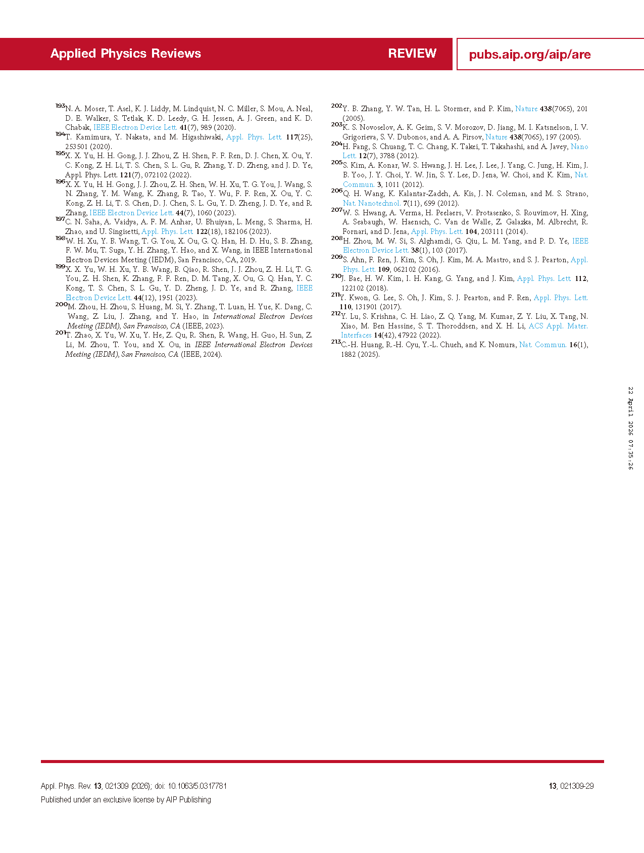
Comprehensively sort out β-Ga₂O₃ transistors from architecture to device physics, integrating three core technical paths of lateral, vertical, and heterogeneous integration;
Systematically summarize the latest progress of four device systems: lateral power MOSFETs (homoepitaxy, heterogeneous integration, circuit applications), vertical power MOSFETs (CAVET, trench gate, FinFET), RF devices, and thin-film transistors;
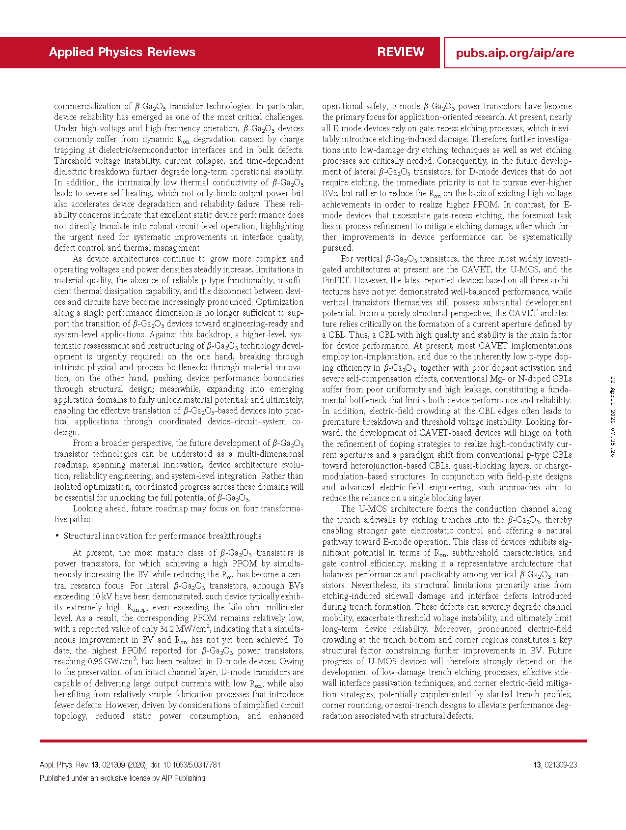
Clarify the performance benchmark of β-Ga₂O₃ devices, pointing out that they have surpassed silicon-based devices and approached the limit of silicon carbide-based devices, revealing the intrinsic potential of materials;
Propose four future development paths: structural innovation for performance breakthroughs, material innovation to overcome bottlenecks, application innovation to expand scenarios, and circuit integration for practical applications.
Conclusion
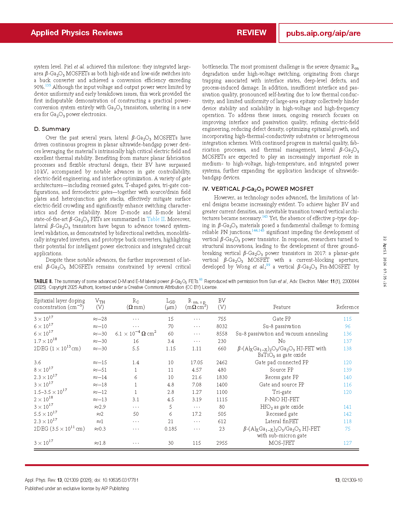
Over the past several years, lateral β-Ga₂O₃ MOSFETs have driven continuous progress in planar ultrawide-bandgap power devices leveraging the material’s intrinsically high critical electric field and excellent thermal stability. Benefiting from mature planar fabrication processes and flexible structural design, their BV have surpassed 10kV, accompanied by notable advances in gate controllability, electric-field engineering, and interface optimization. A variety of gate architectures—including recessed gates, T-shaped gates, tri-gate configurations, and ferroelectric gates—together with source/drain field plates and heterojunction gate stacks, effectively mitigate surface electric-field crowding and significantly enhance switching characteristics and device reliability. Moreover, lateral β-Ga₂O₃ transistors have begun to advance toward system-level validation, as demonstrated by bidirectional switches, monolithically integrated inverters, and prototype buck converters, highlighting their potential for intelligent power electronics and integrated circuit applications.
Despite these notable advances, the further improvement of lateral β-Ga₂O₃ MOSFETs remains constrained by several critical bottlenecks. The most prominent challenge is the severe dynamic Ron degradation under high-voltage switching, originating from charge trapping associated with interface states, deep-level defects, and process-induced damage. In addition, insufficient interface and passivation quality, pronounced self-heating due to low thermal conductivity, and limited uniformity of large-area epitaxy collectively hinder device stability and scalability in high-voltage and high-frequency operation. To address these issues, ongoing research focuses on improving interface and passivation quality, refining electric-field engineering, reducing defect density, optimizing epitaxial growth, and incorporating high-thermal-conductivity substrates or heterogeneous integration schemes. With continued progress in material quality, fabrication processes, and thermal management, lateral β-Ga₂O₃ MOSFETs are expected to play an increasingly important role in medium- to high-voltage, high-temperature, and integrated power systems, further expanding the application landscape of ultrawide-bandgap devices.
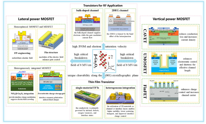
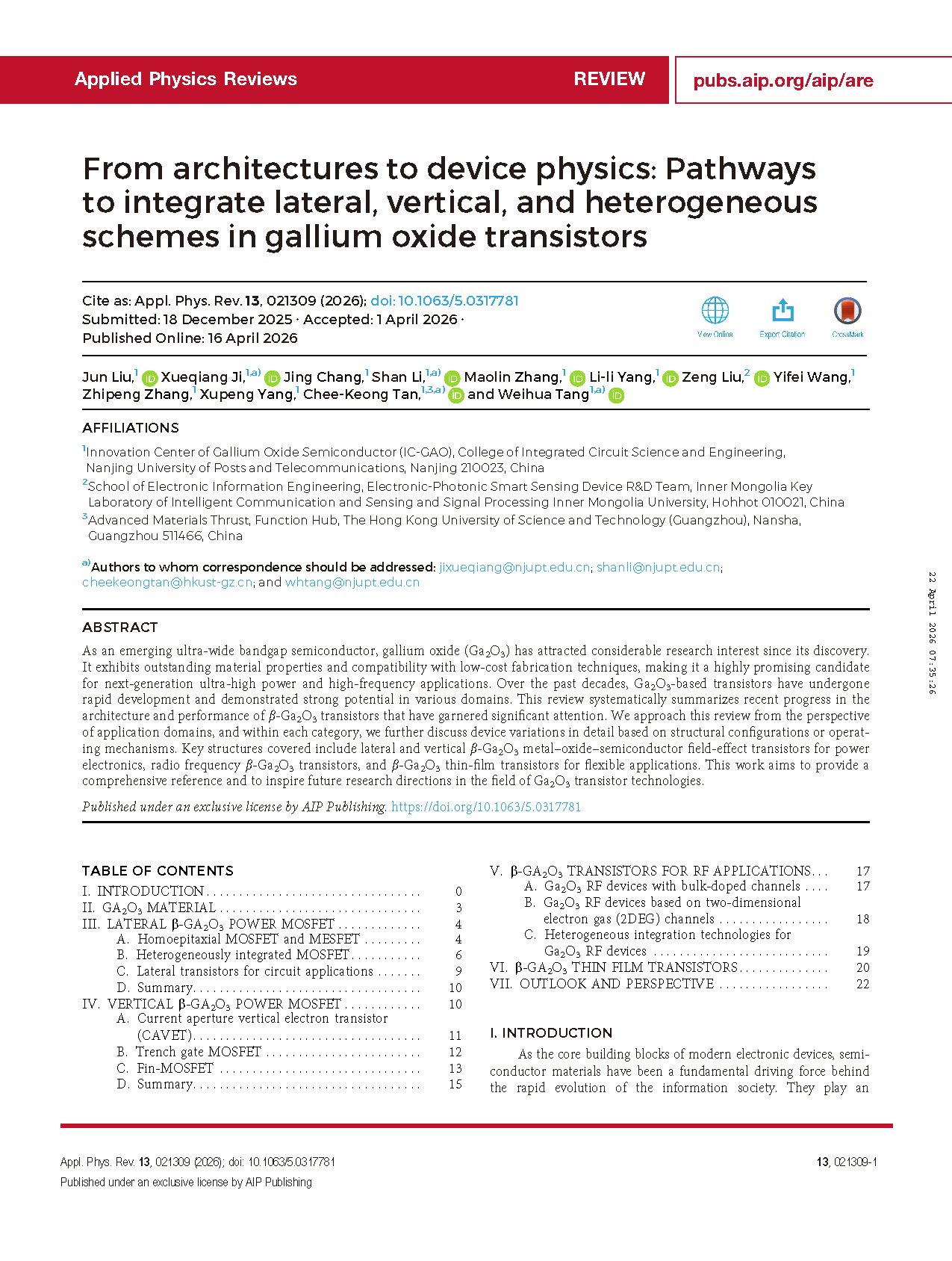
Fig. 1 Structures and physical mechanism of Ga₂O₃ transistors.
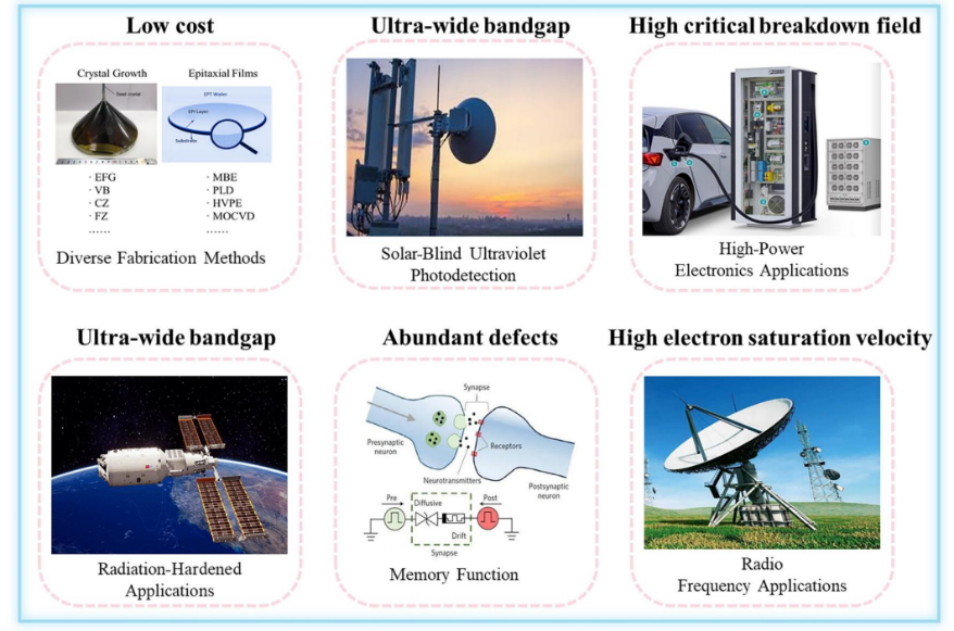
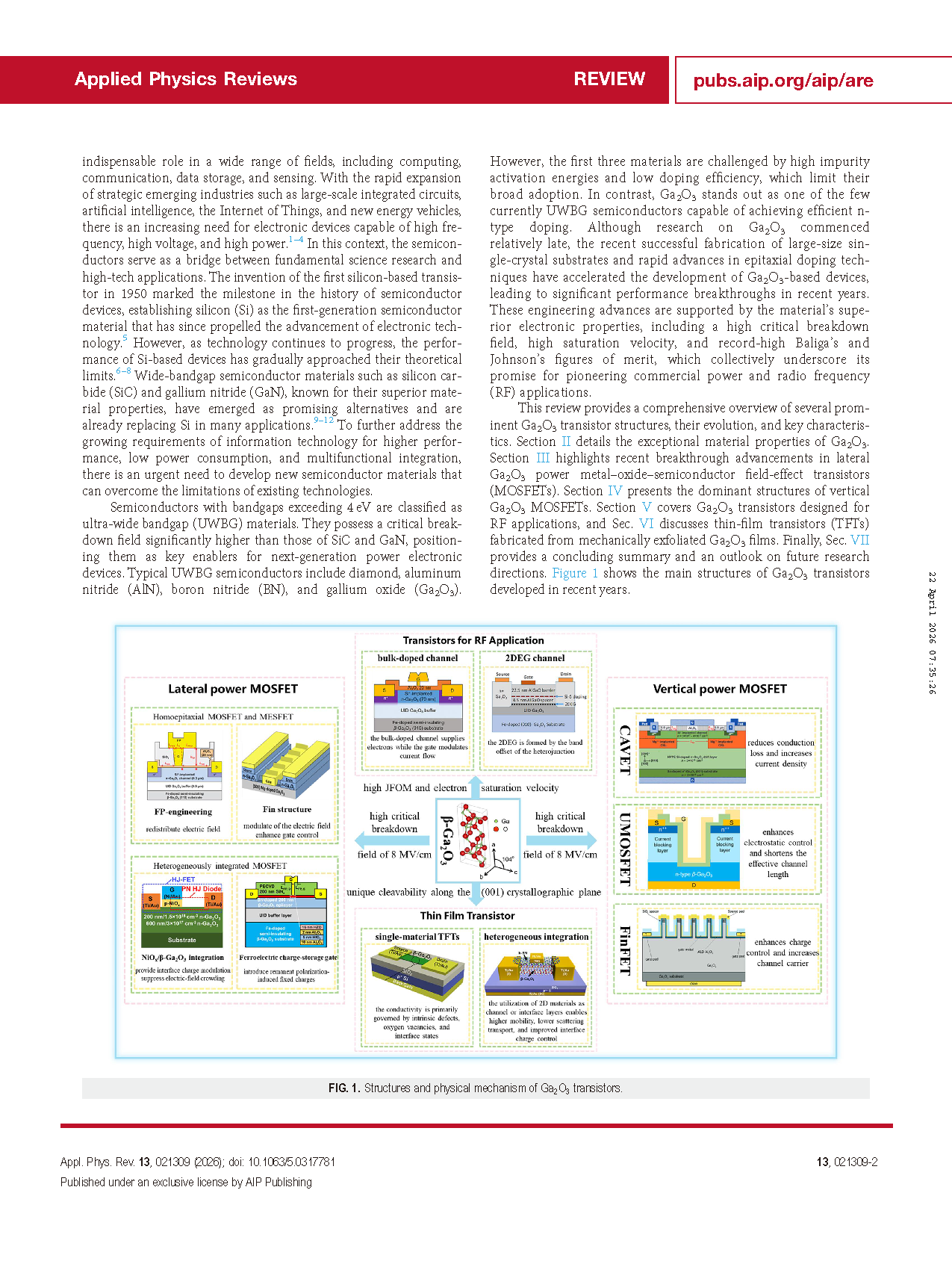
Fig. 2 Currently advance applications in Ga₂O₃.
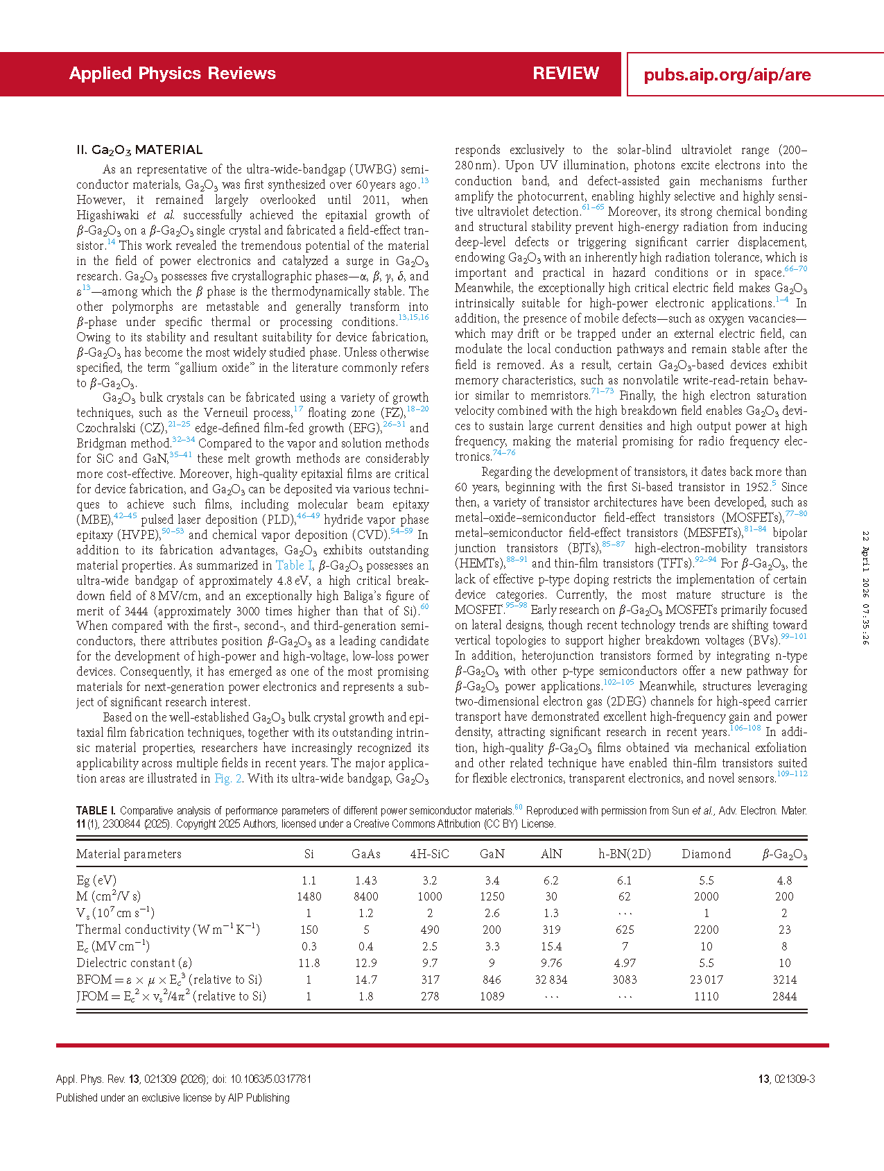
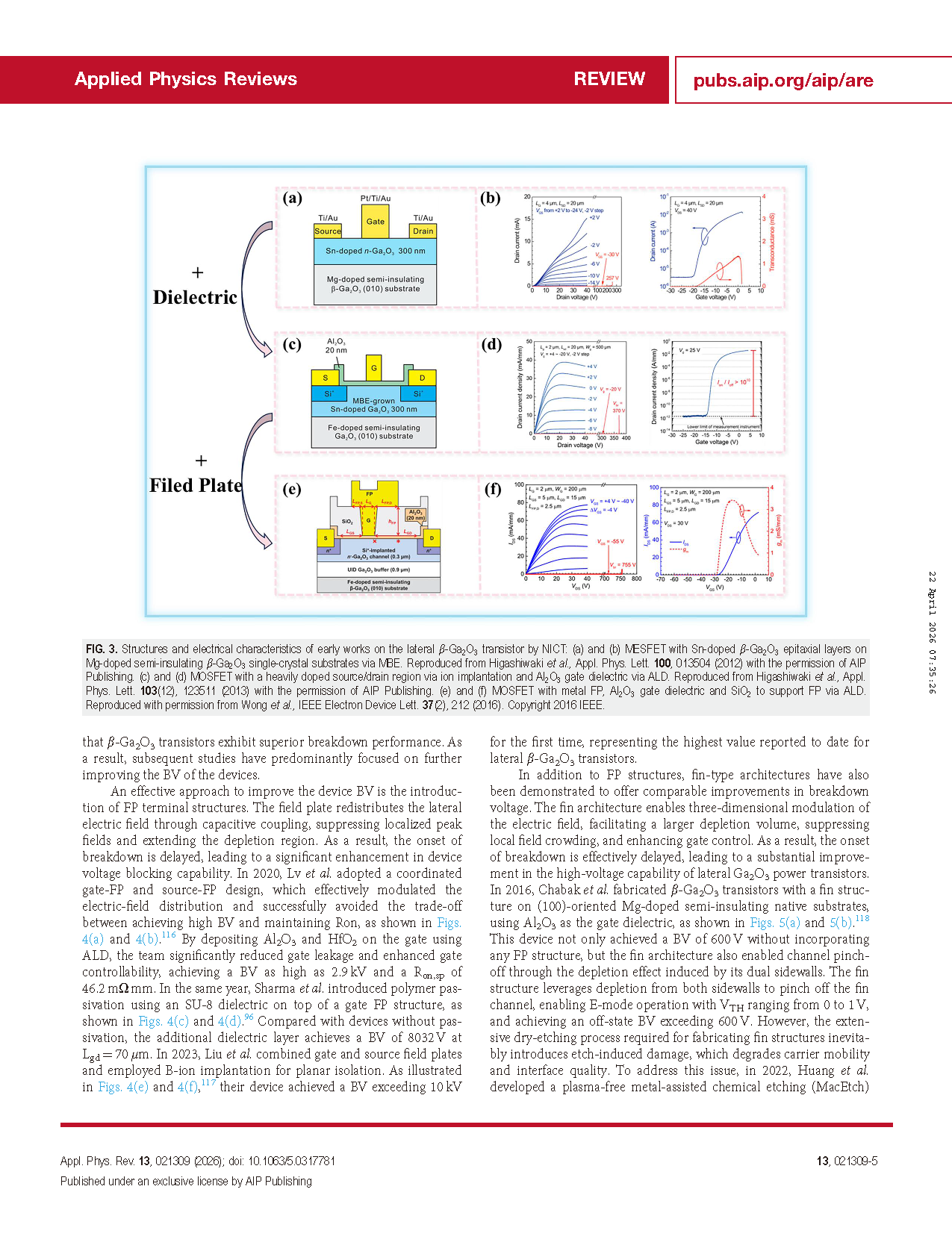
Fig. 3 Structures and electrical characteristics of early works on the lateral Mg-doped semi-insulating β-Ga₂O₃ transistor by NICT: (a) and (b) MESFET with Sn-doped β-Ga₂O₃ epitaxial layers. (c) and (d) MOSFET with a heavily doped source/drain region via ion implantation and Al₂O₃ gate dielectric via ALD. (e) and (f) MOSFET with metal FP, Al₂O₃ gate dielectric and SiO₂ to support FP via ALD.
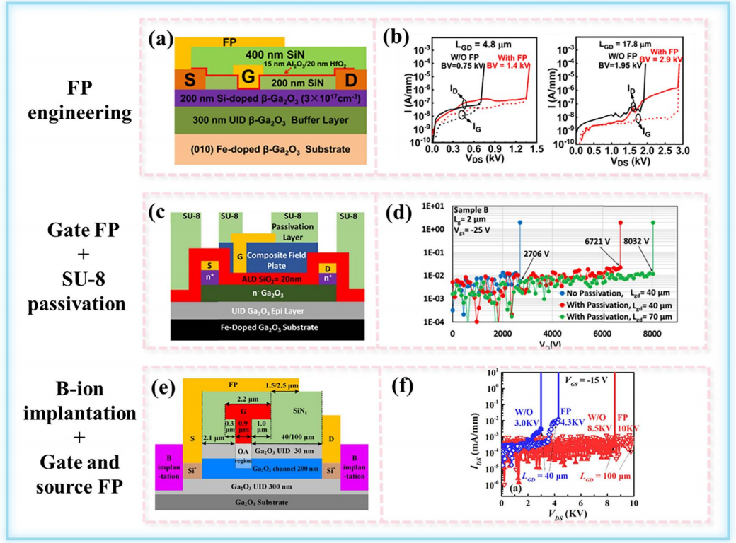
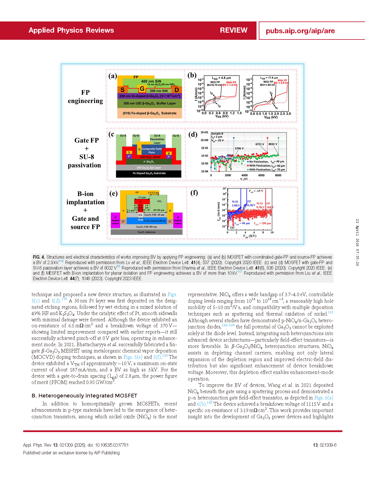
Fig. 4 Structures and electrical characteristics of works improving BV by applying FP engineering: (a) and (b) MOSFET with coordinated gate-FP and source-FP achieves a BV of 2.9 kV. (c) and (d) MOSFET with gate-FP and SU-8 passivation layer achieves a BV of 8032 V. (e) and (f) MESFET with B-ion implantation for planar isolation and FP engineering achieves a BV of more than 10 kV.
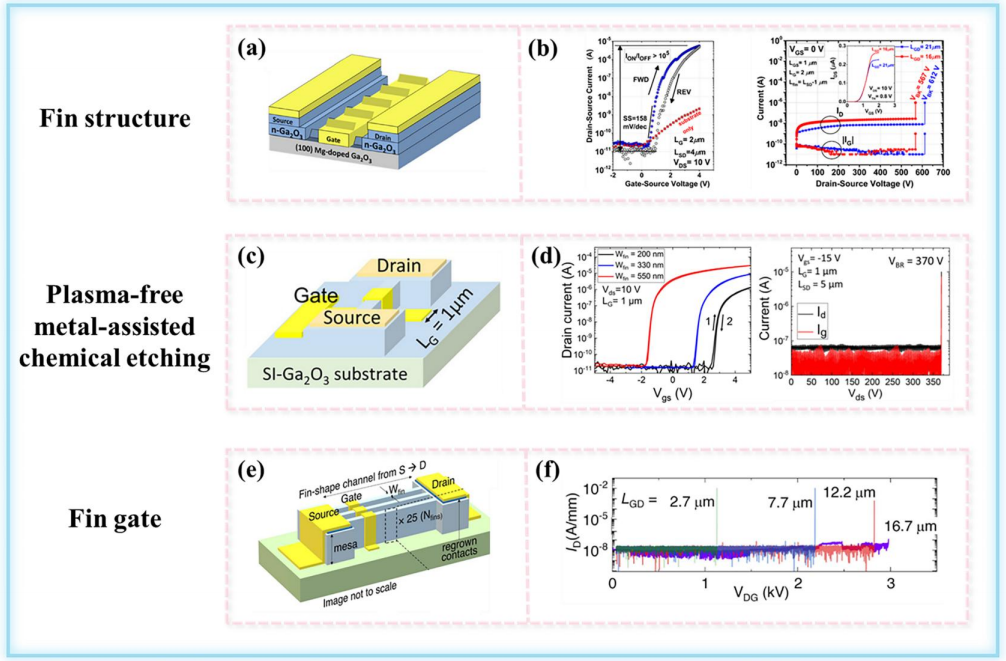
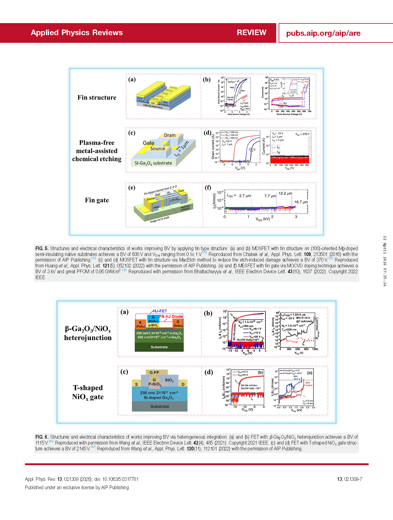
Fig. 5 Structures and electrical characteristics of works improving BV by applying fin type structure: (a) and (b) MOSFET with fin structure on (100)-oriented Mg-doped semi-insulating native substrates achieves a BV of 600 V and VTH ranging from 0 to 1 V. (c) and (d) MOSFET with fin structure via MacEtch method to reduce the etch-induced damage achieves a BV of 370 V. (e) and (f) MESFET with fin gate via MOCVD doping technique achieves a BV of 3 kV and great PFOM of 0.95 GW/cm².
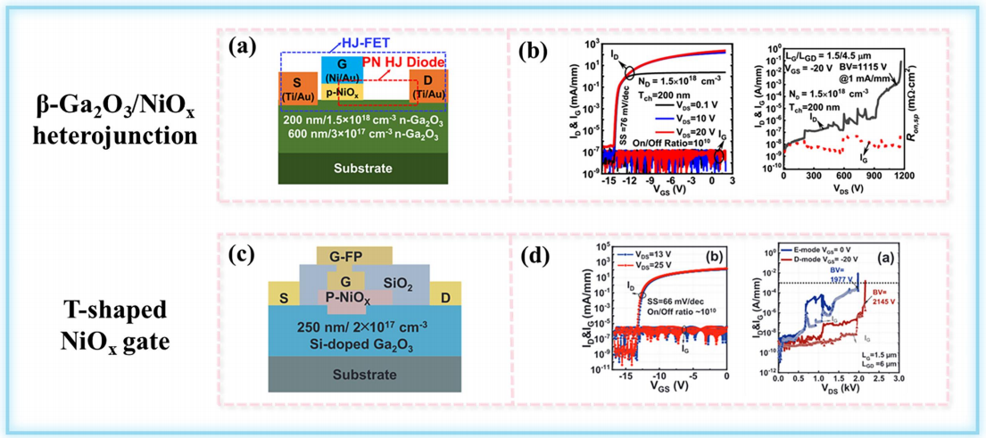
Fig. 6 Structures and electrical characteristics of works improving BV via heterogeneous integration: (a) and (b) FET with β-Ga₂O₃/NiOₓ heterojunction achieves a breakdown voltage of 1115 V. (c) and (d) FET with T-shaped NiOₓ gate structure achieves a breakdown voltage of 2145 V.
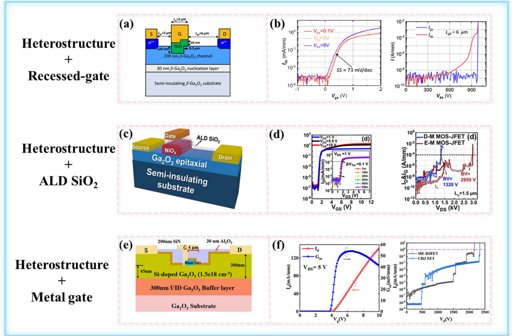
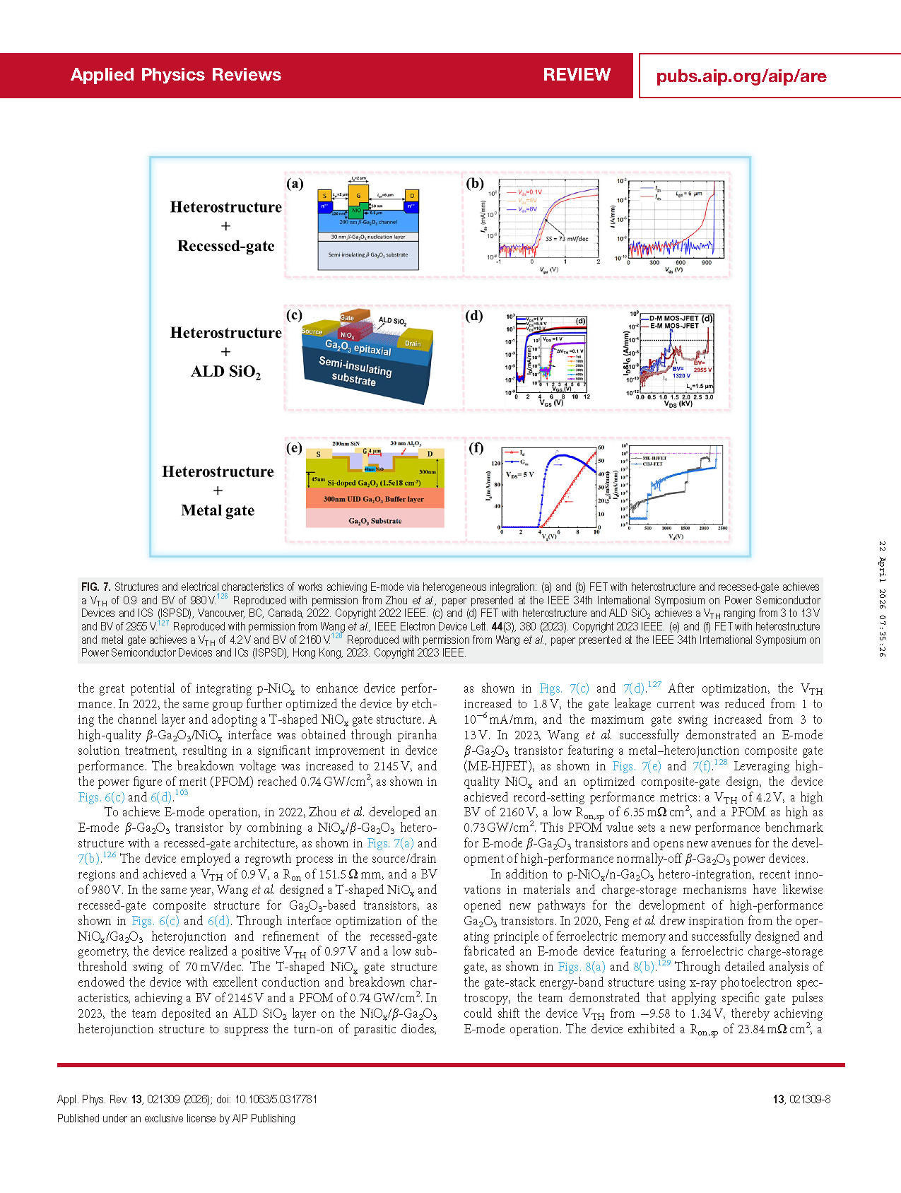
Fig. 7 Structures and electrical characteristics of works achieving E-mode via heterogeneous integration: (a) and (b) FET with heterostructure and recessed-gate achieves a VTH of 0.9 V and BV of 980 V. (c) and (d) FET with heterostructure and ALD SiO₂ achieves a VTH ranging from 3 to 13 V and BV of 2955 V. (e) and (f) FET with heterostructure and metal gate achieves a VTH of 4.2 V and BV of 2160 V.
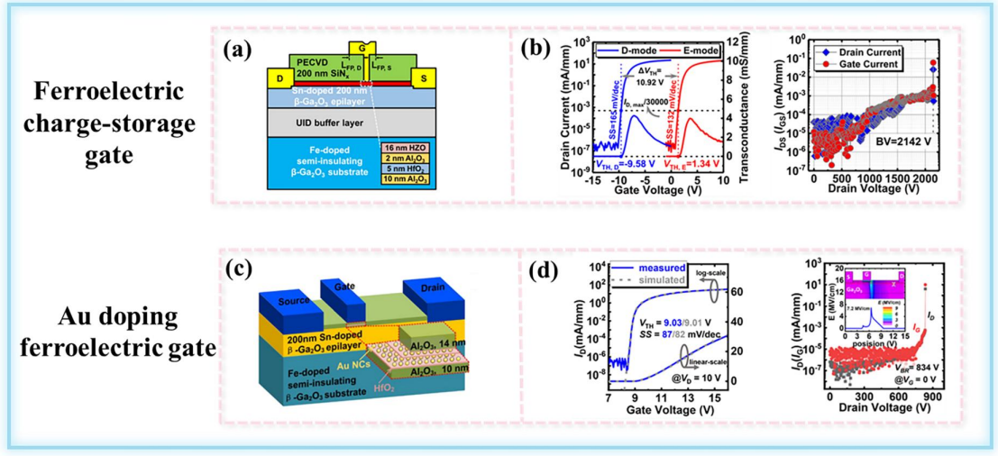
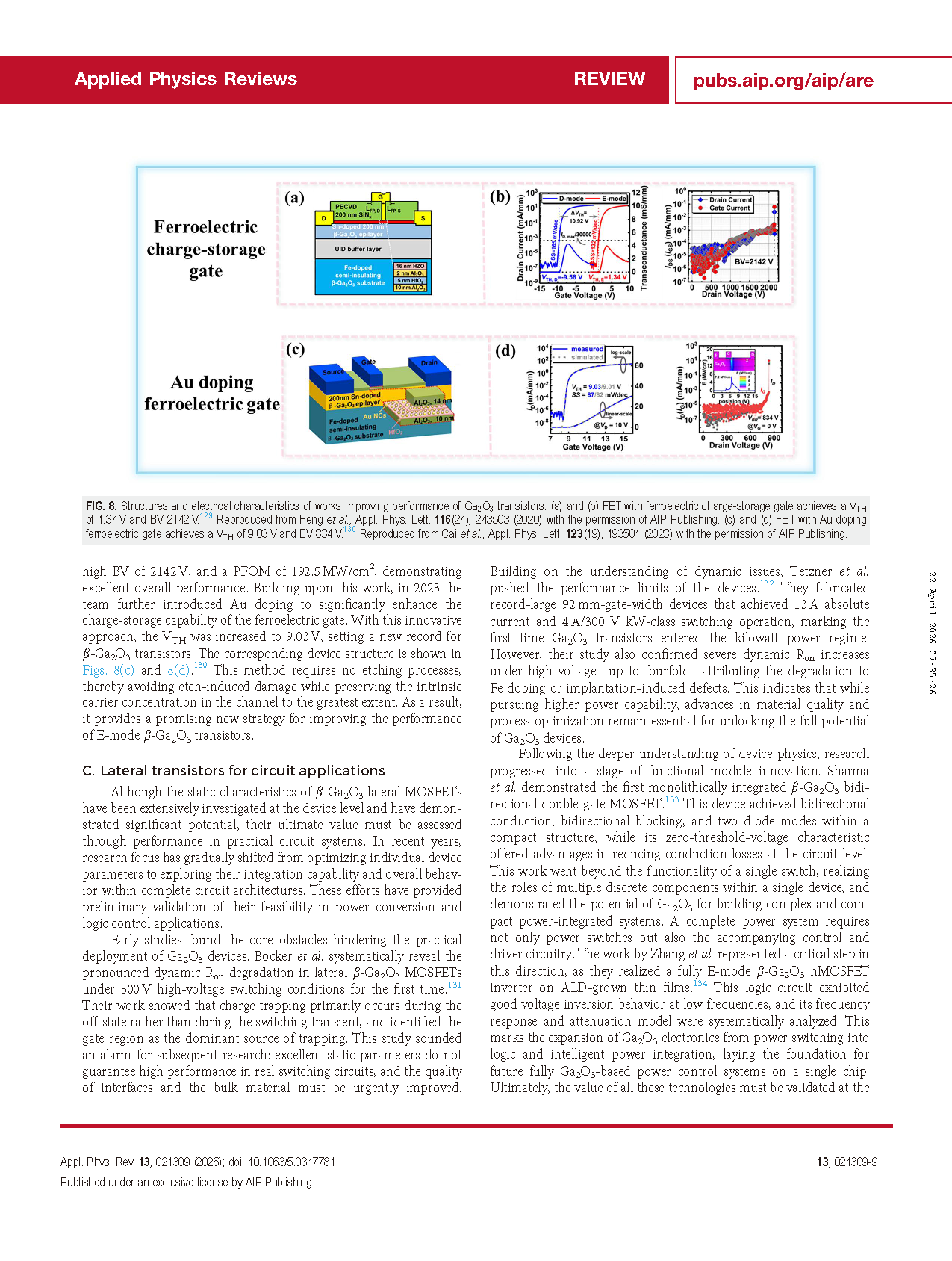
Fig. 8 Structures and electrical characteristics of works improving performance of Ga₂O₃ transistors: (a) and (b) FET with ferroelectric charge-storage gate achieves a VTH of 1.34 V and BV 2142 V. (c) and (d) FET with Au doping ferroelectric gate achieves a VTH of 9.03 V and BV 834 V.
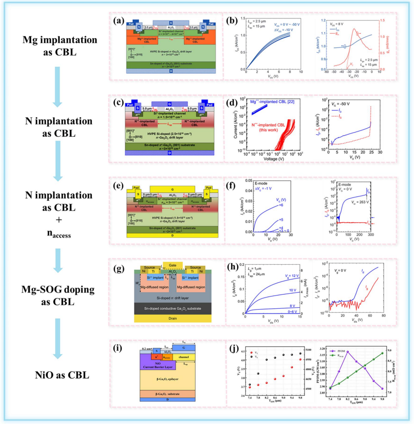
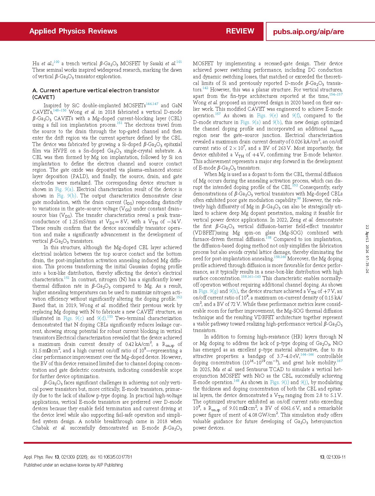
Fig. 9 Structures and electrical characteristics of works for the development of vertical β-Ga₂O₃ MOSFET with CBL type: (a) and (b) CAVET with Mg-ion implantation as CBL achieves a VTH of -34 V. (c) and (d) CAVET with N-ion implantation as CBL achieves a maximum drain current density of 0.42 kA/cm². (e) and (f) CAVET with N-ion implantation as CBL and the addition of n access achieves a VTH of 4 V and BV of 263 V. (g) and (h) VDBFET with Mg-SOG selective doping as CBL achieves a VTH of 7 V and maximum on-current density of 0.15 kA/cm². (i) and (j) CAVET with NiO as CBL via TCAD simulation achieves a VTH ranging from 2.8 to 5.1 V and BV of 6061.6 V.
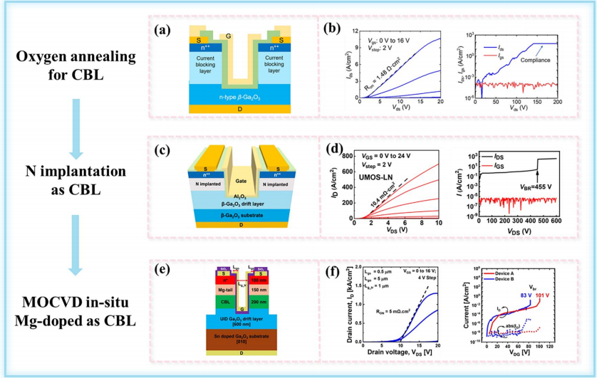
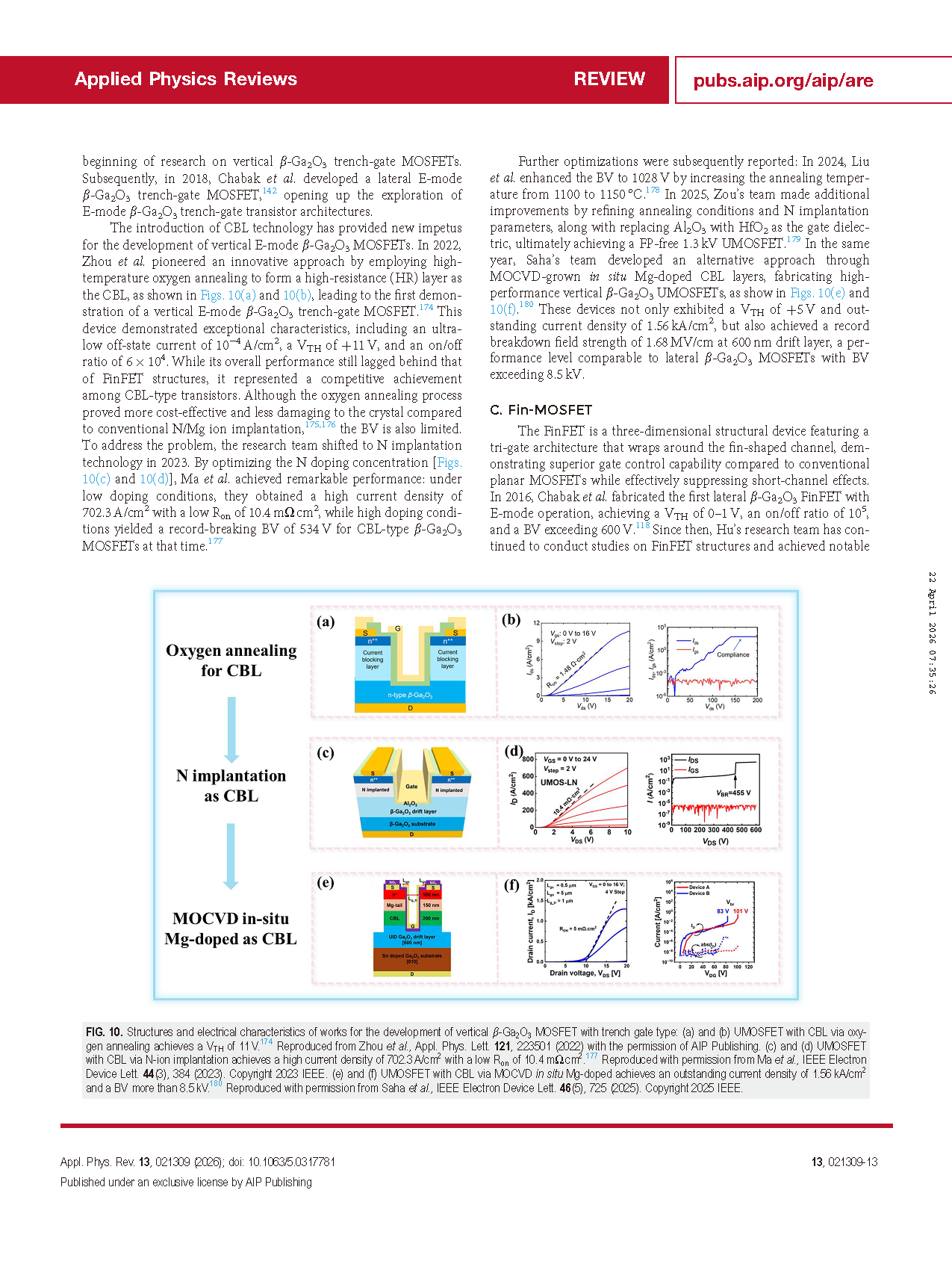
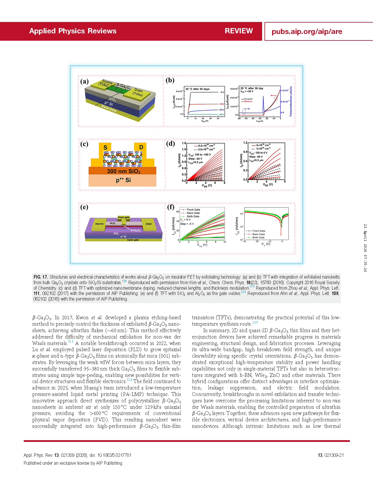
Fig. 10 Structures and electrical characteristics of works for the development of vertical β-Ga₂O₃ MOSFET with trench gate type: (a) and (b) UMOSFET with CBL via oxygen annealing achieves a VTH of 11 V. (c) and (d) UMOSFET with CBL via N-ion implantation achieves a high current density of 702.3 A/cm² with a low Ron of 10.4 mΩ cm². (e) and (f) UMOSFET with CBL via MOCVD in-situ Mg-doped achieves an outstanding current density of 1.56 kA/cm² and a BV more than 8.5 kV.
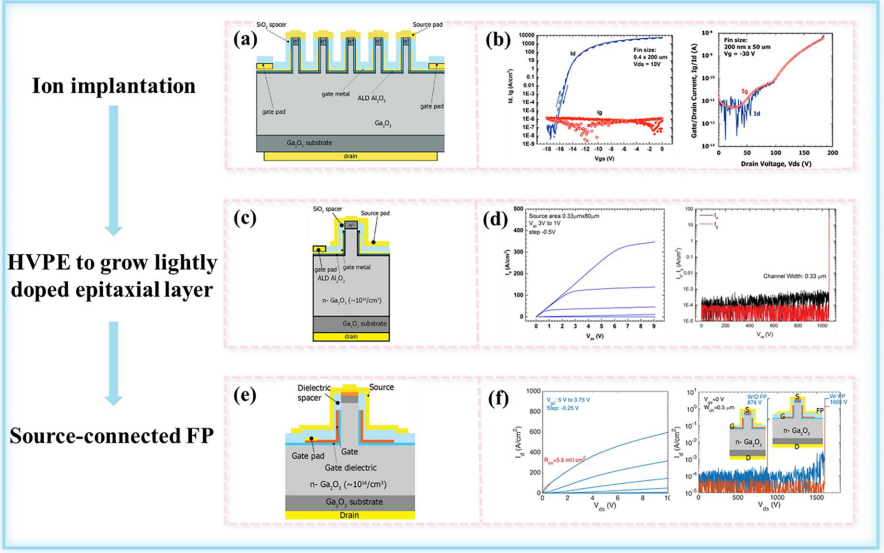
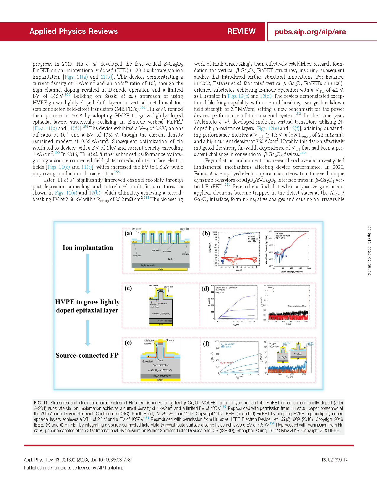
Fig. 11 Structures and electrical characteristics of Hu’s team’s works of vertical β-Ga₂O₃ MOSFET with fin type: (a) and (b) FinFET on an unintentionally doped (UID) (−201) substrate via ion implantation achieves a current density of 1 kA/cm² and a limited BV of 185 V. (c) and (d) FinFET by adopting HVPE to grow lightly doped epitaxial layers achieves a VTH of 2.2 V and a BV of 1057 V. (e) and (f) FinFET by integrating a source-connected field plate to redistribute surface electric fields achieves a BV of 1.6 kV.
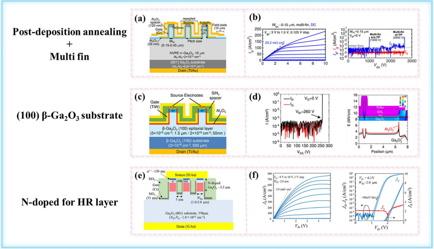
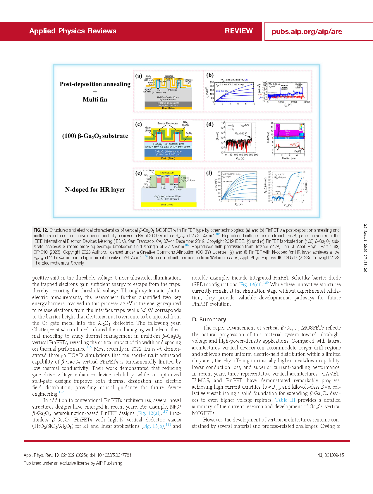
Fig. 12 Structures and electrical characteristics of vertical β-Ga₂O₃ MOSFET with FinFET type by other technologies: (a) and (b) FinFET via post-deposition annealing and multi fin structures to improve channel mobility achieves a BV of 2.66 kV with a Ron,sp of 25.2 mΩ cm². (c) and (d) FinFET fabricated on (100) β-Ga₂O₃ substrate achieves a record-breaking average breakdown field strength of 2.7 MV/cm. (e) and (f) FinFET with N-doped for HR layer achieves a low Ron,sp of 2.9 mΩ cm² and a high current density of 760 A/cm².
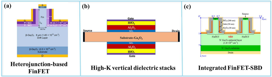
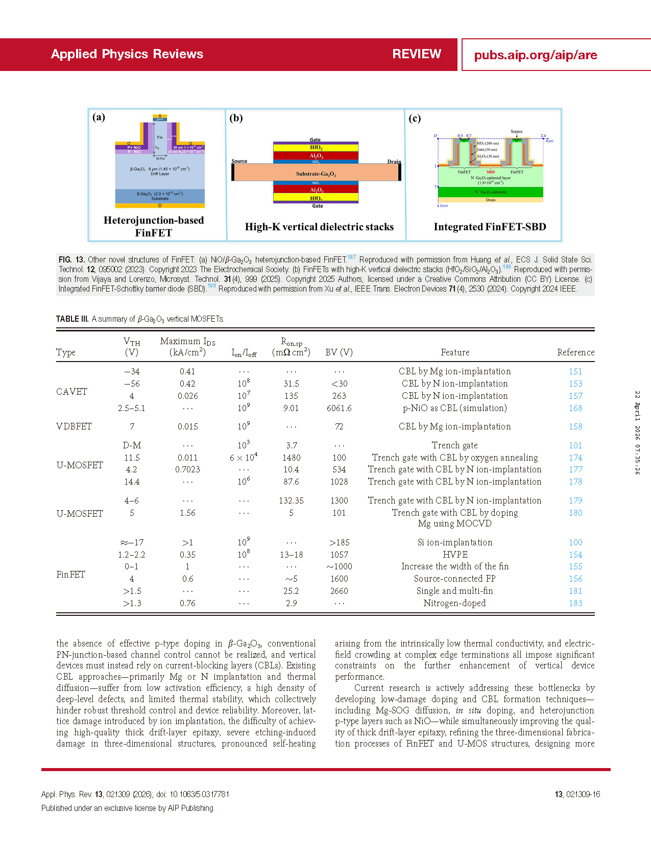
Fig. 13 Other novel structures of FinFET: (a) NiO/β-Ga₂O₃ heterojunction-based FinFET. (b) FinFETs with high-K vertical dielectric stacks (HfO₂/SiO₂/Al₂O₃). (c) Integrated FinFET-Schottky barrier diode (SBD).
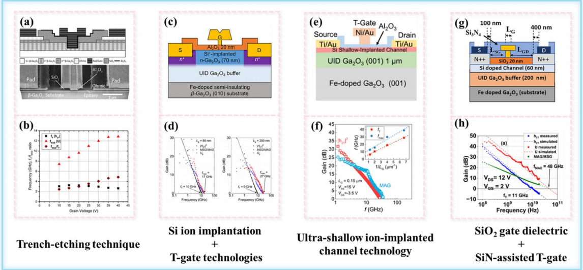
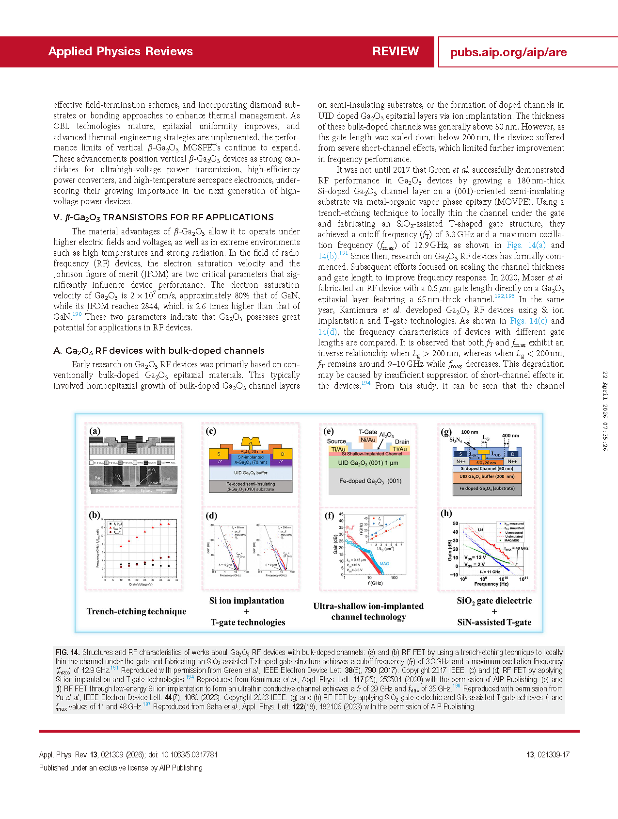
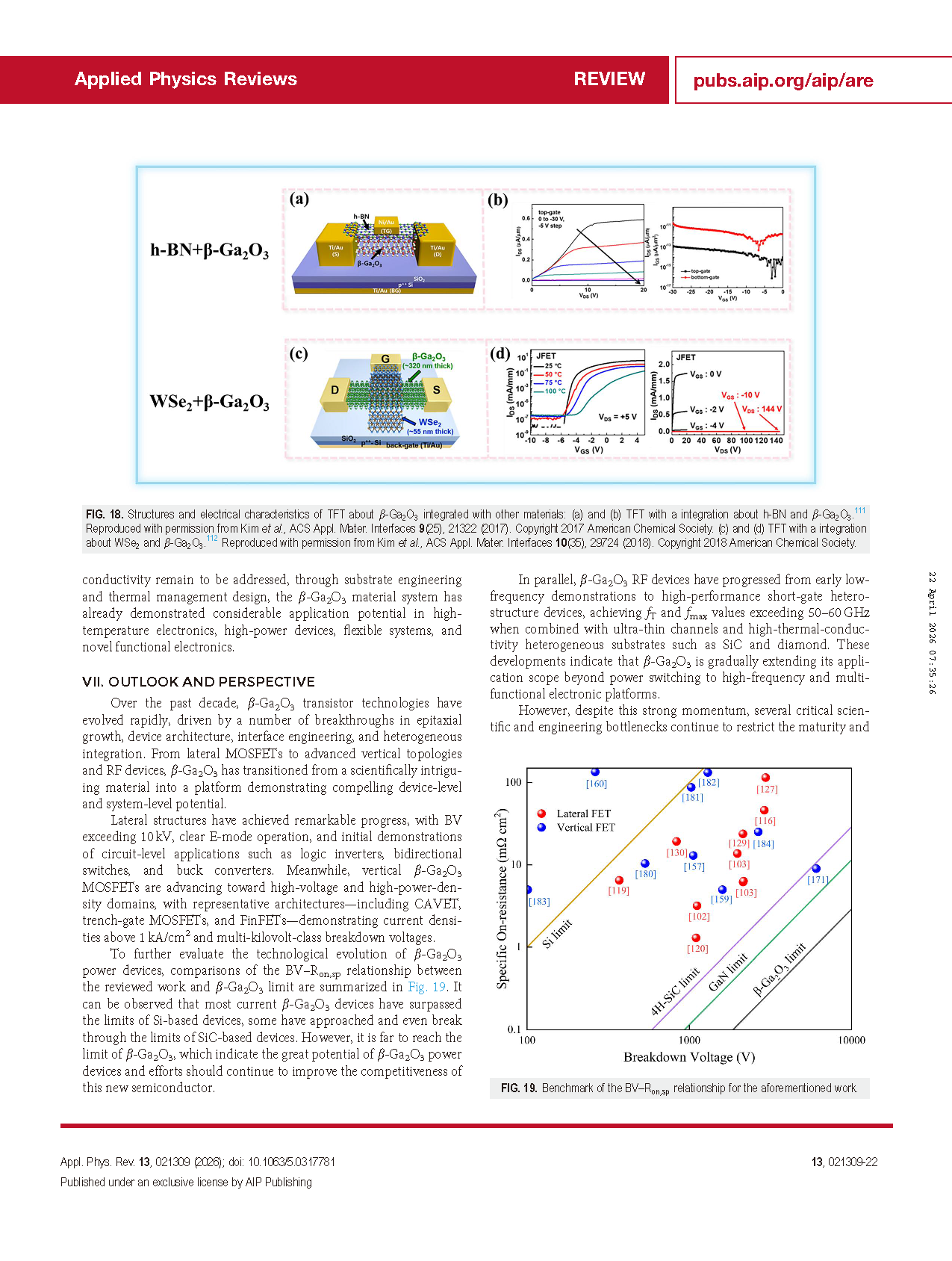
Fig. 14 Structures and RF characteristics of works about Ga₂O₃ RF devices with bulk-doped channels: (a) and (b) RF FET by using a trench-etching technique to locally thin the channel under the gate and fabricating an SiO₂-assisted T-shaped gate structure achieves a cutoff frequency (fT) of 3.3 GHz and a maximum oscillation frequency (fmax) of 12.9 GHz. (c) and (d) RF FET by applying Si-ion implantation and T-gate technologies. (e) and (f) RF FET through low-energy Si ion implantation to form an ultrathin conductive channel achieves a fT of 29 GHz and fmax of 35 GHz. (g) and (h) RF FET by applying SiO₂ gate dielectric and SiN-assisted T-gate achieves fT and fmax values of 11 and 48 GHz.
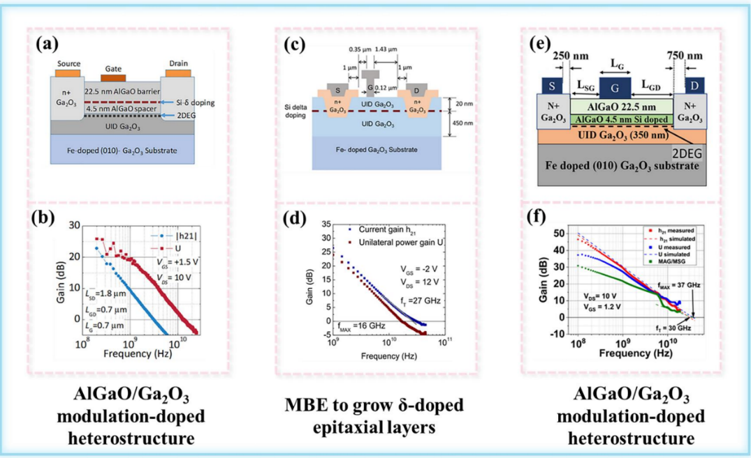
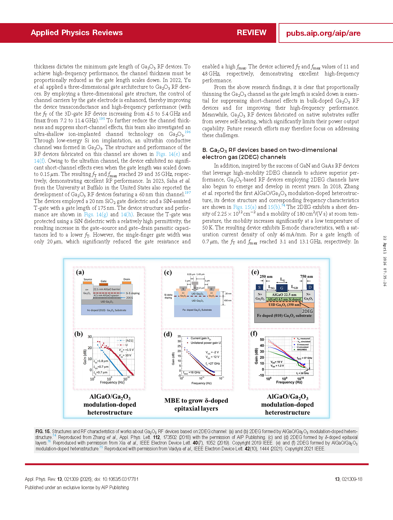
Fig. 15 Structures and RF characteristics of works about Ga₂O₃ RF devices based on 2DEG channel: (a) and (b) 2DEG formed by AlGaO/Ga₂O₃ modulation-doped heterostructure. (c) and (d) 2DEG formed by δ-doped epitaxial layers. (e) and (f) 2DEG formed by AlGaO/Ga₂O₃ modulation-doped heterostructure.
DOI :
10.1063/5.0317781