Paper Sharing
【Member Papers】Edge-Dependent Stacking Fault Upward Transformation in Pseudo-Symmetric (100) β-Ga₂O₃ HVPE Epitaxy: A Common Source of Hillocks
日期:2026-05-09阅读:48
Researchers from the Zhejiang University have published a dissertation titled "Edge-Dependent Stacking Fault Upward Transformation in Pseudo-Symmetric (100) β-Ga₂O₃ HVPE Epitaxy: A Common Source of Hillocks" in Acta Materialia.
Background
Beta-phase gallium oxide (β-Ga2O3) is a semiconductor material with ultra-wide bandgap of ∼4.8 eV, high critical breakdown field of 8 MV/cm, and optical absorption edge near 260 nm, making it highly attractive for applications in Schottky barrier diodes (SBDs), metal–oxide–semiconductor field effect transistors (MOSFETs) and solar-blind photoelectric devices. To achieve outstanding performance, the development of device-quality β-Ga2O3 epilayer is imperative. Halide vapor phase epitaxy (HVPE) has been investigated and successfully commercialized due to its much faster growth rate and capability to produce thick epilayers, achieving a dramatic growth rate up to 250 μm/h. To date, HVPE homoepitaxial growth had already been widely explored for (001) and (010) oriented β-Ga2O3 planes. However, HVPE growth on (100) plane, which is a promising plane for commercializing due to its easy size-enlarged and wafer processing, remains largely unexplored.
Abstract
Stacking faults pose a major challenge in the epitaxial growth of β-Ga2O3 thick films on the (100) planes, as they degrade the surface morphology and severely deteriorate the performance of power devices. In this work, we systematically investigate the formation, evolution and electrical influence of stacking faults and related defects in (100) β-Ga2O3 homoepitaxial layers grown by halide vapor phase epitaxy (HVPE). Using multiple characterization techniques, we reveal that the commonly observed stacking fault SF100-B undergoes an edge-dependent upward transformation into out-of-phase boundaries (OPBs) during epitaxial growth. The formation of OPBs directly trigger the nucleation of pyramidal hillocks on the epitaxial surface and act as killer defect, leading to premature breakdown in Schottky barrier diodes. Atomic-scale analysis demonstrates that SF100-B originates from consecutive twinning processes on the pseudo-symmetric (100) plane of β-Ga2O3, whereas its mismatch with the perfect lattice at (-201) facets drives the formation of OPBs. Furthermore, two key parameters, the Ga adatom diffusion lengthand the terrace width, were demonstrated directly related to the formation of SF100-B. Accordingly, two effective strategies, reducing the Ⅵ/Ⅲ ratio and increasing the offcut angle, were developed to suppress stacking faults. The insights gained from this work offer valuable guidance for engineering defect-controlled surfaces to enable high-performance β-Ga2O3-based power electronic devices.
Conclusions
In conclusion, we systematically investigated the origin of pyramidal hillock defects on the [00-1]-offcut (100) β-Ga2O3 epitaxial layer growth by HVPE. It unveils that in addition to dislocations, out-of-phase boundary (OPB) constitutes a new source of hillocks formation. In β-phase homoepitaxial layers, OPBs are formed by shear slip along the translation vector of 1/6[132], leading to in-phase overlapping of octahedron Ga atoms on (100)-A and (100)-B, accompanied by a characteristic overlaid structure. Furthermore, these OPBs were demonstrated to be detrimental to the leakage current of SBD devices, emphasizing the controlling of OPBs during (100) β-Ga2O3 epitaxial growth. Atomic-scale investigations via HRSTEM were performed to elucidate the underlying formation mechanisms of OPBs. We found that the exposed facet at step edge dominates whether the upward transformation of SF100-B yields OPB or SF001, depending on the offcut direction of (100) substrate towards [00-1] or [001]. The formation of SF100-B is driven by an atomic-scale consecutive twinning process on the pseudo-symmetric (100) plane. Subsequently, SF100-B will simultaneously upward transformation into OPB when it impinges with the (-201) step facet of normal lattice, which ultimately gives rise to pyramidal hillocks on the epilayer surface. Therefore, the behavior of stacking faults on the [00-1]-offcut (100) β-Ga2O3 is fully clarified. Moreover, it is proposed that the formation of SF100-B is directly related to the balance between two critical parameters: the Ga adatom diffusion length and the width of terrace. Based on this principle, two corresponding effective strategies, lower Ⅵ/Ⅲ ratios (e.g., VI/III=10) and larger offcut angles (up to 6°), were developed to achieve hillock-free (100) β-Ga2O3 epitaxy.
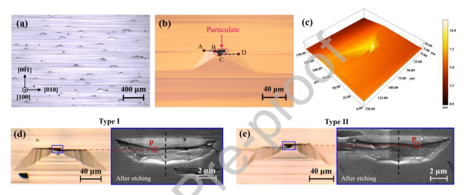
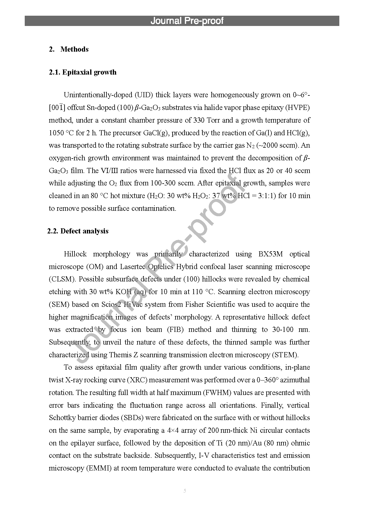
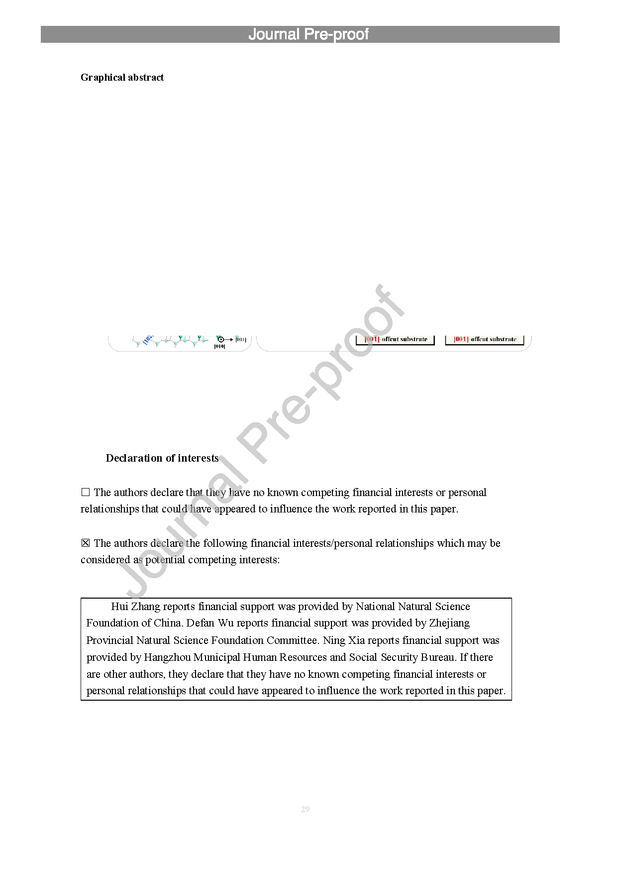
Fig. 1. (a) OM image of pyramid hillock defects on HVPE epilayer grown on 4°-offcut (100) β-Ga2O3 substrate, (b) DIC-OM image of a representative pyramid hillock defect on (a), (c) CLSM 3D image for the pyramid hillock defect shown in (b). (d-e) DIC-OM images of two types of pyramid hillock defects and corresponding SEM images taken at the blue framed region after CMP and subsequent preferential etching.
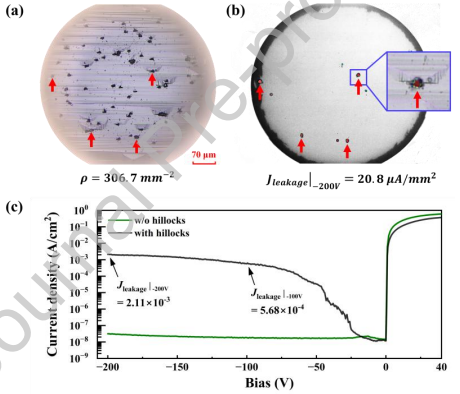
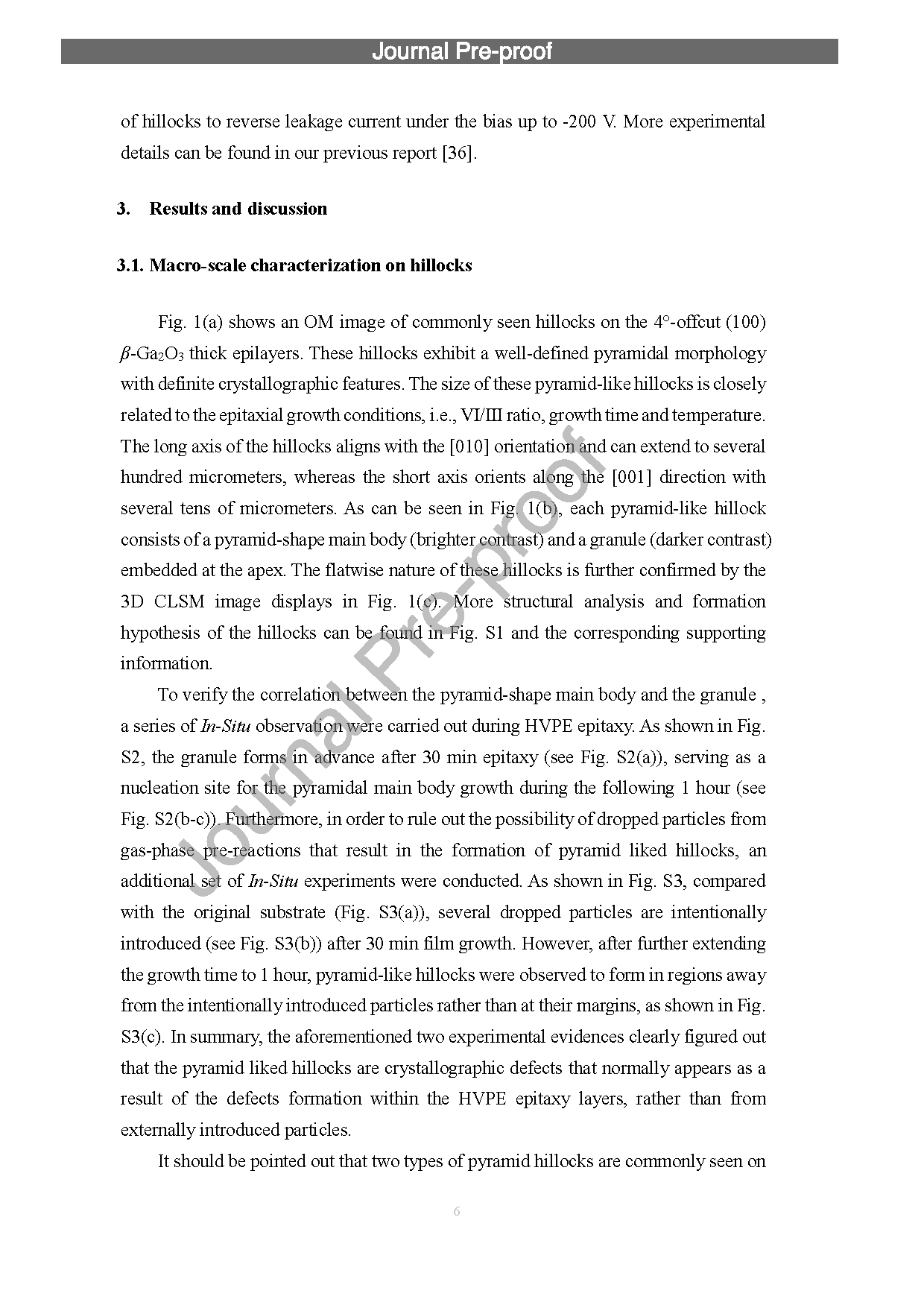
Fig. 2. (a) Mirror-flipped OM image of hillock rich area selected for SBD fabrication, (b) In-situ emission microscopy (EMMI) image of leakage current under the SBD device, the enlarged image on the right shows the overlapping of the OM and the EMMI results. (c) I-V characteristics of the SBD shown in (b), compared with another SBD without pyramids residing on the same surface.
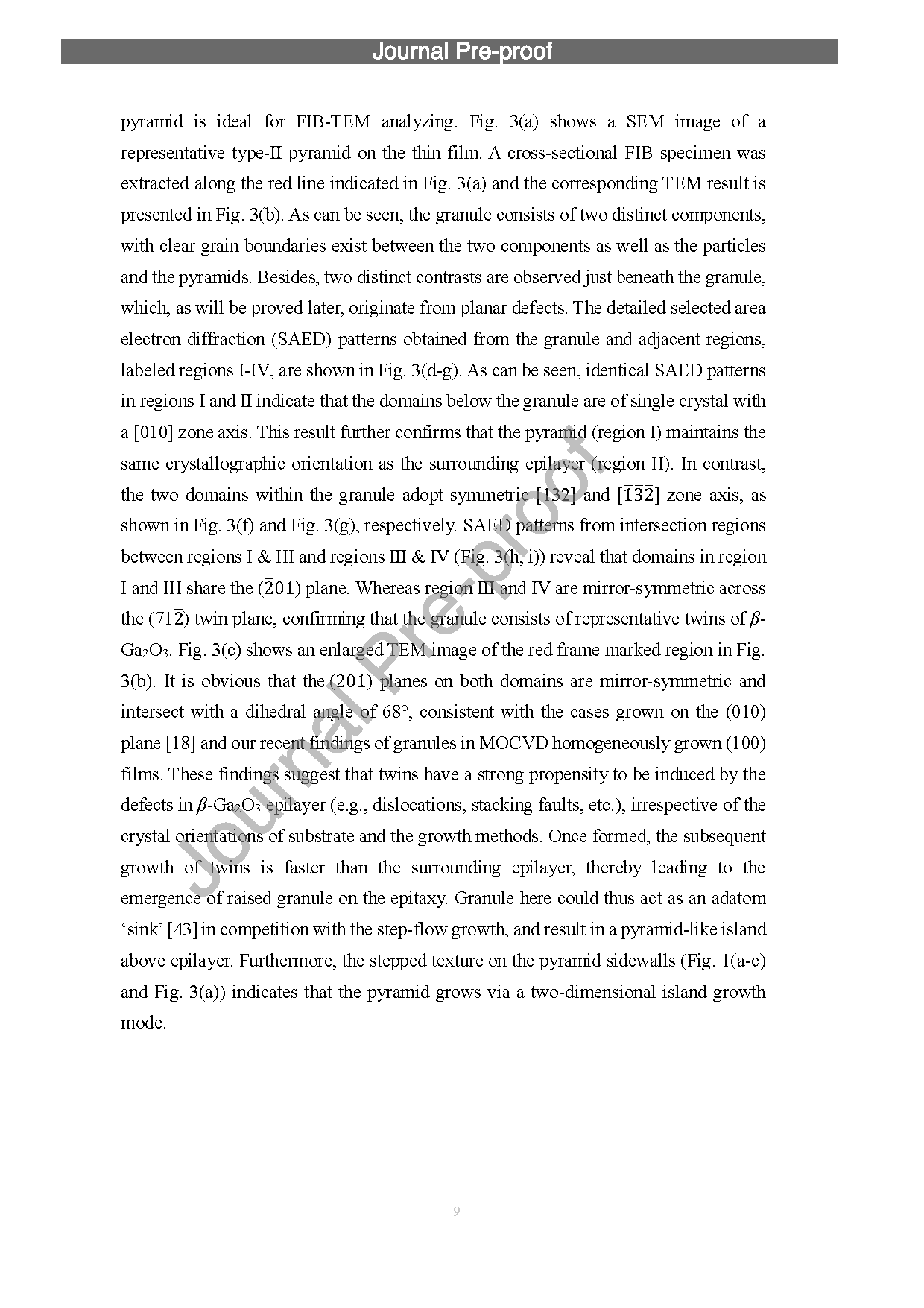
Fig. 3. (a) SEM image of a typical pyramid hillock on a 30 min HVPE growth thin films, (b) Cross-sectional TEM image of the lamella extracted from (a) along the red dashed line, (c) The enlarged TEM image taken from the red framed region in (b), and (d-i) SAED patterns obtained at regions Ⅰ- Ⅳ, Ⅰ∩Ⅲ, Ⅲ∩Ⅳ, respectively.
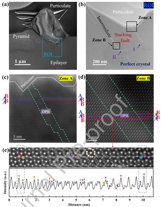
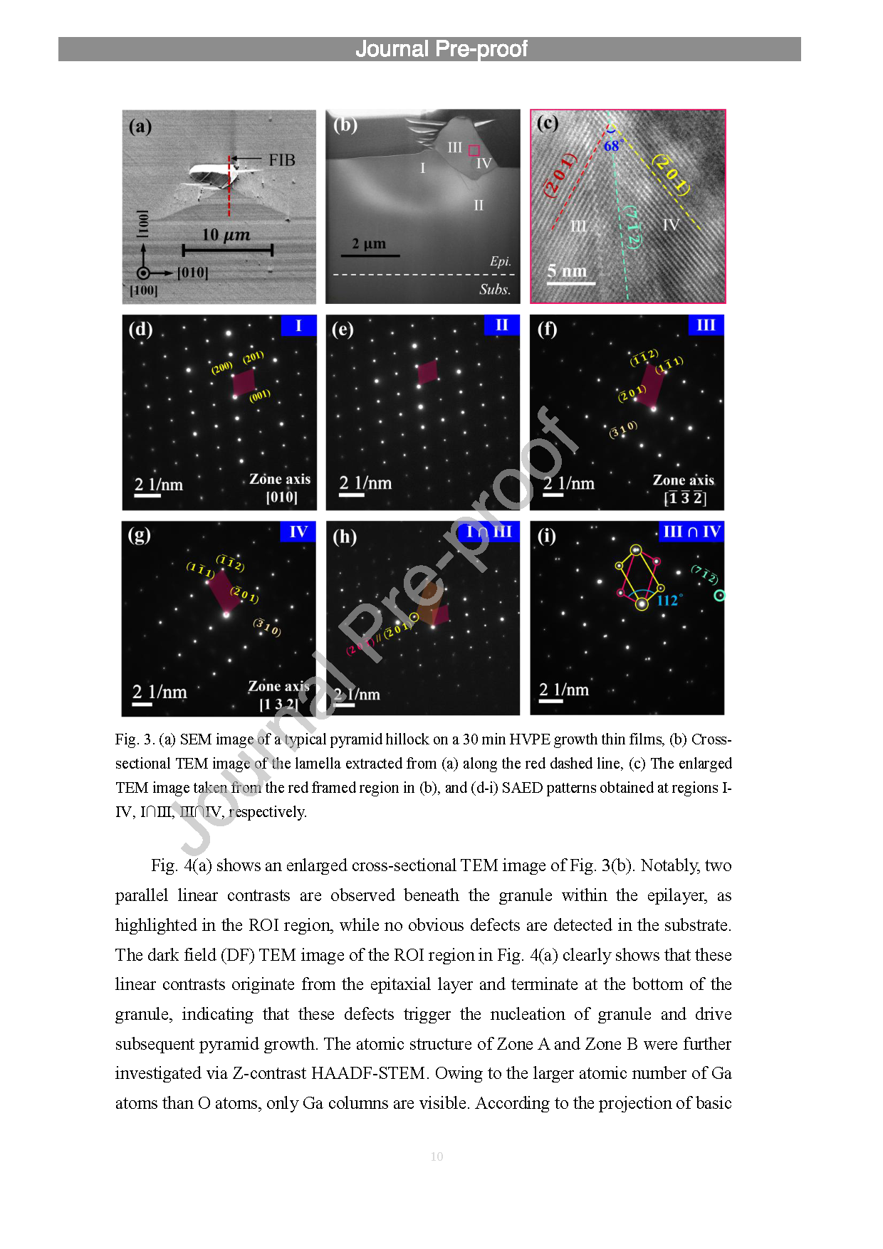
Fig. 4. (a) Cross-sectional TEM image of the granule and the threading defects beneath it, (b) The amplfied TEM image of the ROI region denoted in (a), (c-d) HRSTEM images of Zone A and Zone B of (b), (e) Enlarged STEM image of the red framed region shown in (c) and the linear intensity along the white dash line.
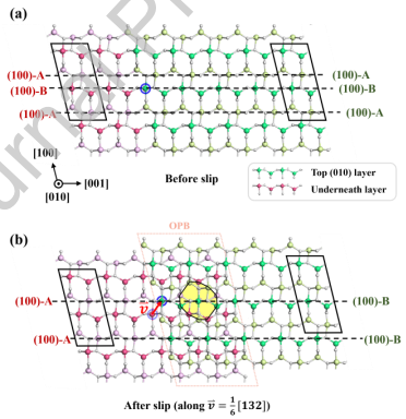
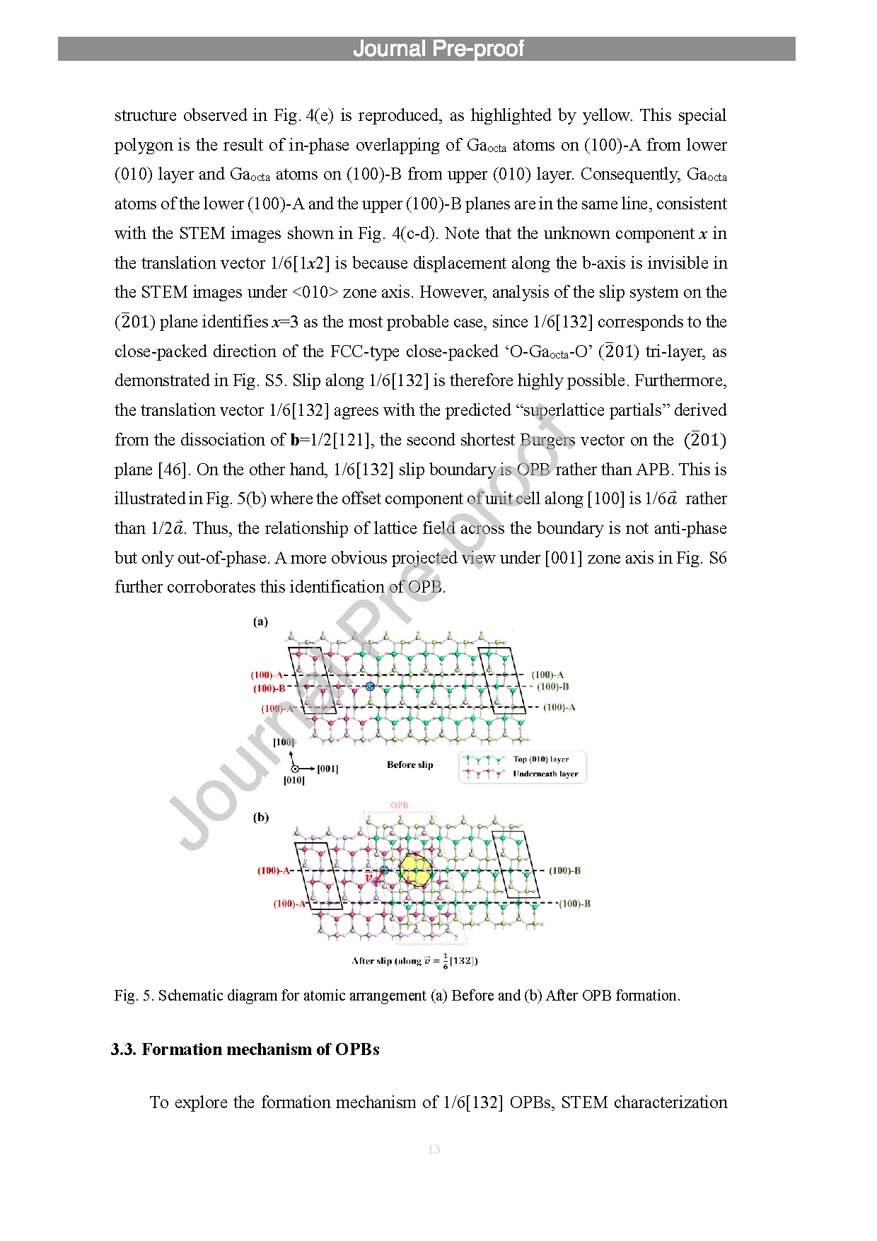
Fig. 5. Schematic diagram for atomic arrangement (a) Before and (b) After OPB formation.
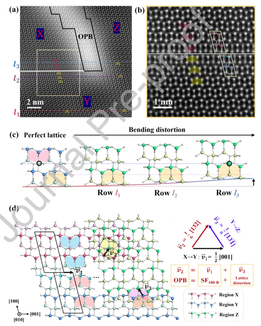
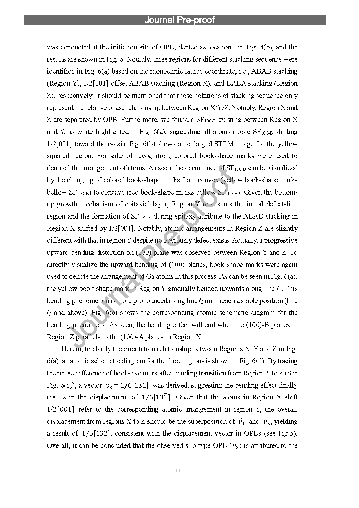
Fig. 6. (a) HRSTEM image acquired at location I in Fig. 4(b), (b) Enlarged HRSTEM image of the boundary between Region X and Region Y in (a), (c) Atomic schematic diagram for the bending phenomena shown in (a) and (d) Atomic schematic diagram for the three regions with their corresponding phase difference.
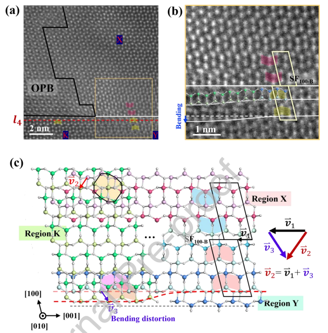
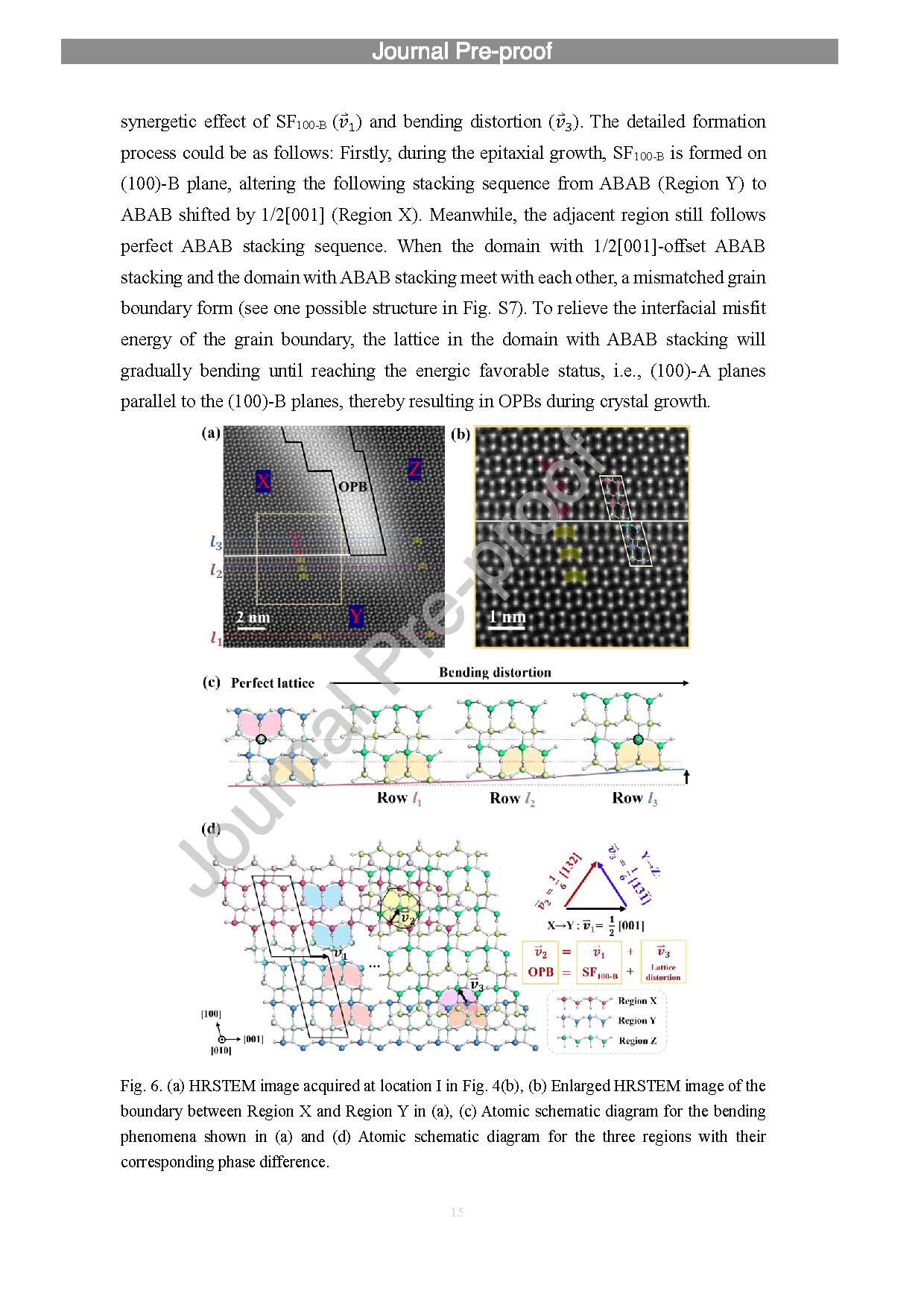
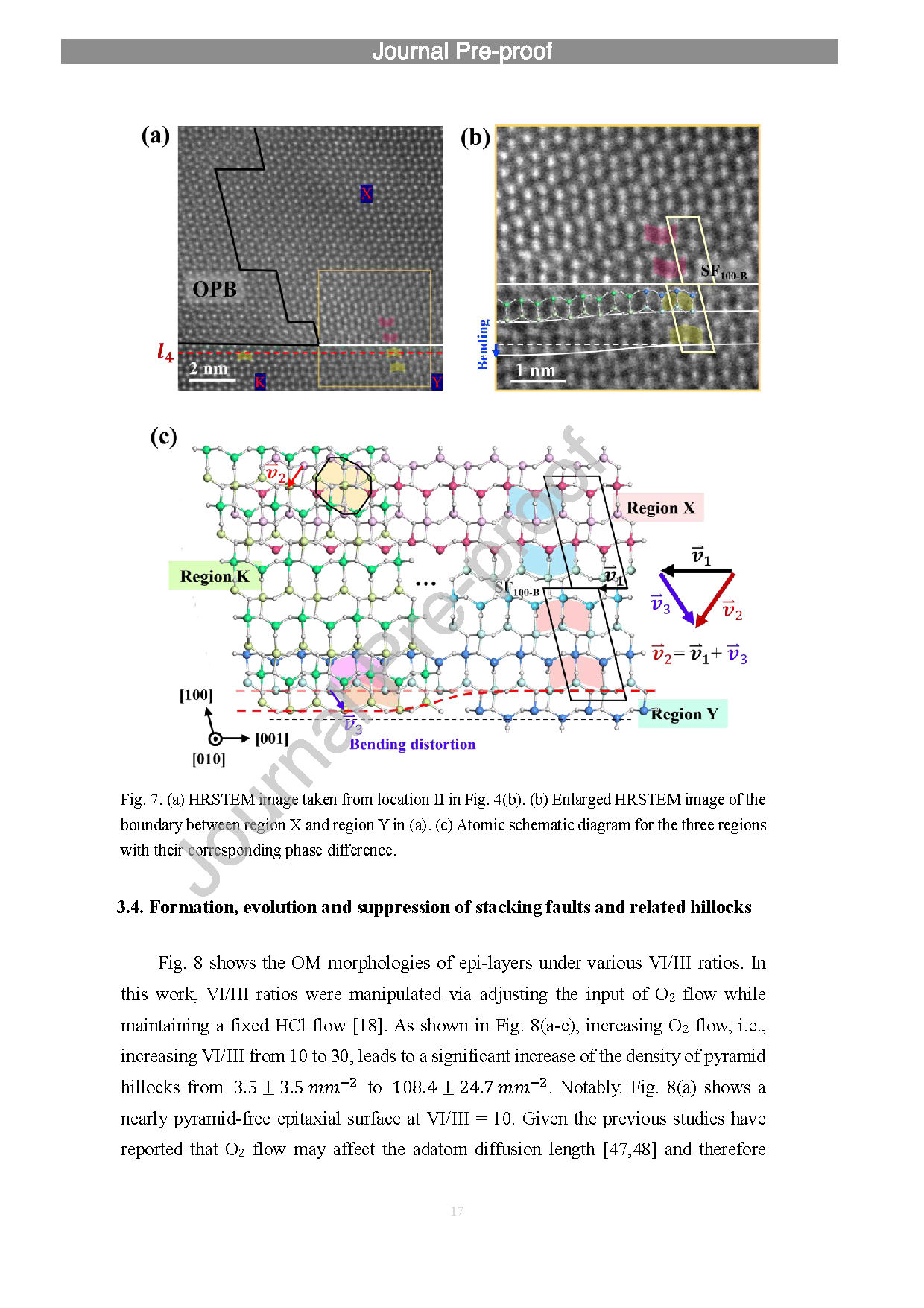
Fig. 7. (a) HRSTEM image taken from location Ⅱ in Fig. 4(b). (b) Enlarged HRSTEM image of the boundary between region X and region Y in (a). (c) Atomic schematic diagram for the three regions with their corresponding phase difference.
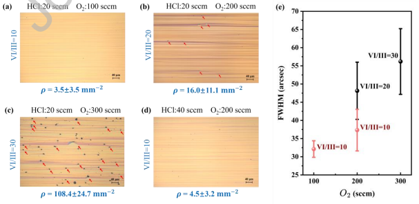
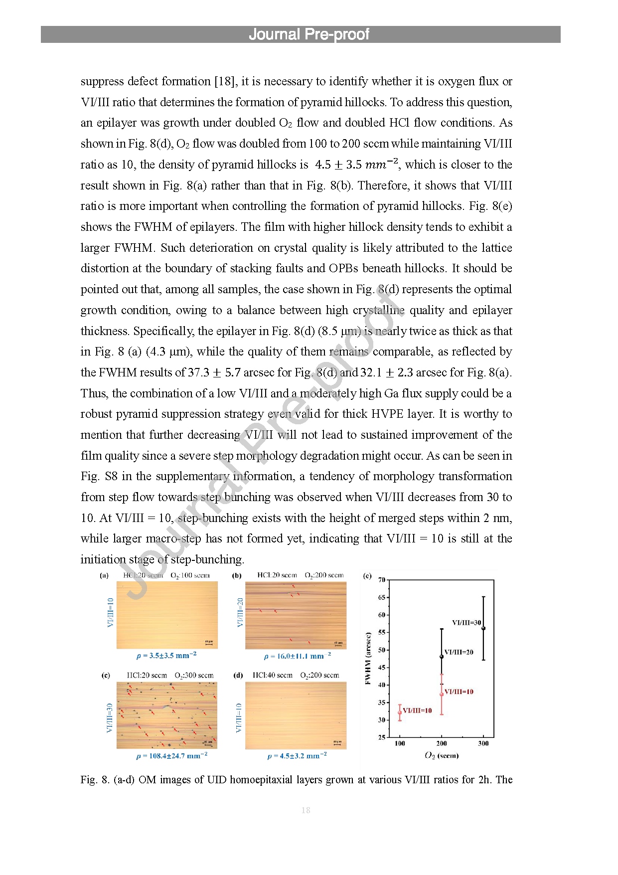
Fig. 8. (a-d) OM images of UID homoepitaxial layers grown at various VI/III ratios for 2h. The pyramid is marked by red arrows. (e) Corresponding FWHM of films shown in (a-d).
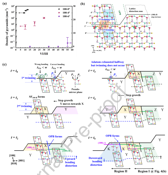
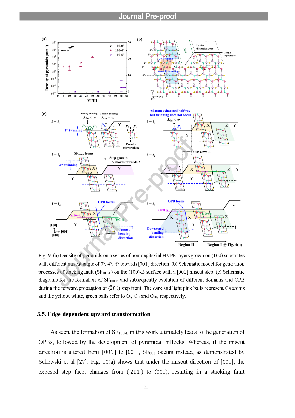
Fig. 9. (a) Density of pyramids on a series of homoepitaxial HVPE layers grown on (100) substrates with different miscut angle of 0°, 4°, 6° towards [00-1] direction. (b) Schematic model for generation processes of stacking fault (SF100-B) on the (100)-B surface with a [00-1] miscut step. (c) Schematic diagrams for the formation of SF100-B and subsequently evolution of different domains and OPB during the forward propagtion of (-201) step front. The dark and light pink balls represent Ga atoms and the yellow, white, green balls refer to OI, OII and OIII, respectively.
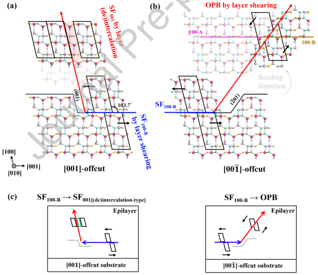
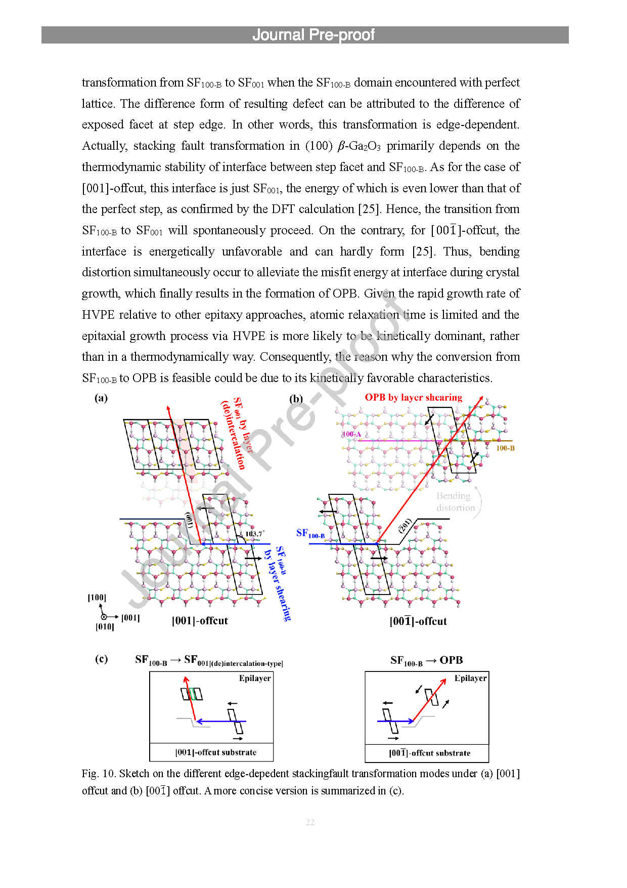
Fig. 10. Sketch on the different edge-depedent stackingfault transformation modes under (a) [001] offcut and (b) [00-1] offcut. A more concise version is summarized in (c).
DOI:
doi.org/10.1016/j.actamat.2026.122315