


Paper Sharing
【International Papers】Direct fabrication of diamond films on β-Ga₂O₃ using Q-carbon
日期:2026-05-20阅读:168
β-Ga₂O₃, as an emerging ultra-wide bandgap (UWBG) semiconductor material, possesses a bandgap of approximately 4.8 eV, a high critical electric field, and an excellent Baliga figure of merit, demonstrating significant potential in high-power and high-frequency electronic devices. Its substrates can be fabricated through melt-growth techniques, enabling low-cost and large-area production. However, the relatively low thermal conductivity of β-Ga₂O₃ (11–27 W/m·K) leads to severe self-heating effects, limiting device power density and reliability.
Diamond, with its exceptionally high thermal conductivity (~2000 W/m·K), is considered an ideal thermal management material. Nevertheless, directly growing high-quality diamond films on β-Ga₂O₃ remains challenging due to surface energy mismatch, thermal stress, substrate decomposition, and poor interfacial adhesion. Conventional approaches, such as nanoparticle seeding or buffer layers, have been explored, but they often introduce additional thermal resistance or fail to fundamentally resolve adhesion and nucleation issues.
Recently, a research team from Texas State University proposed a new approach for the direct growth of high-quality diamond films on β-Ga₂O₃ surfaces using a Q-carbon interlayer. The related work was published in the journal Materials Science in Semiconductor Processing under the title Direct fabrication of diamond films on β-Ga₂O₃ using Q-carbon.
Research Framework and Core Concept
The study follows a clear process route. First, high-quality β-Ga₂O₃ thin films were prepared on c-Al₂O₃ substrates via pulsed laser deposition (PLD). Subsequently, a diamond-like carbon (DLC) layer was deposited, followed by nanosecond pulsed laser annealing (PLA) to in-situ form a Q-carbon interlayer on the β-Ga₂O₃ surface. Finally, diamond films were grown using hot-filament chemical vapor deposition (HFCVD).
Q-carbon is a metastable carbon phase formed under ultrafast laser melting and extreme undercooling conditions. Rich in sp³-bonded diamond-like tetrahedral structures, it exhibits high nucleation density and strong interfacial bonding capability with the substrate. By simulating laser-material interactions (SLIM), the researchers optimized the laser energy density (~0.4 J/cm²) and achieved a controllable melt regrowth velocity (~12.5 m/s), enabling the formation of a uniform Q-carbon layer.
This interlayer not only mitigates island-like growth caused by surface energy mismatch, but also promotes atomic hydrogen etching of sp² carbon during the HFCVD process, thereby accelerating high-quality diamond nucleation and columnar growth. At the same time, it alleviates thermal mismatch stress and prevents film cracking or delamination.
Main Findings and Conclusions
Experimental results demonstrated that the diamond films grown using the Q-carbon seed layer exhibited a sharp Raman characteristic peak at 1332.6 cm⁻¹ with a narrow full width at half maximum (FWHM) of only 9.28 cm⁻¹, indicating low graphitic content and high crystal quality. The films also formed well-faceted structures with fivefold twinning.
Compared with diamond films directly grown on β-Ga₂O₃ or sapphire substrates, the stress level was reduced by approximately 70%–75%, while film adhesion was significantly enhanced without obvious delamination. Cross-sectional analysis further confirmed the formation of columnar diamond structures, which are beneficial for efficient heat transport. Simulation results agreed well with experimental observations, validating the physical mechanism of Q-carbon formation.
The paper concludes that the Q-carbon interlayer provides a simple, economical, and effective route for integrating diamond with β-Ga₂O₃. It overcomes the limitations of conventional seeding or buffer-layer methods and enables the fabrication of large-area, continuous, high-quality diamond films without significantly increasing interfacial thermal resistance.
This approach is expected to advance front-side thermal management for β-Ga₂O₃-based high-power devices and may also provide a reference for heterogeneous integration between diamond and other ultra-wide bandgap semiconductors.
Significance of the Research
This work carries important implications for the field of ultra-wide bandgap power electronics. By effectively addressing thermal management bottlenecks, it lays the foundation for improving the power density, reliability, and operating temperature range of β-Ga₂O₃ devices.
Meanwhile, the potential of Q-carbon as a universal nucleation layer opens new possibilities for diamond integration on a broader range of non-carbide substrates. In the future, this technology could be further integrated with device fabrication processes, supporting the development of next-generation high-performance power electronic and optoelectronic devices.
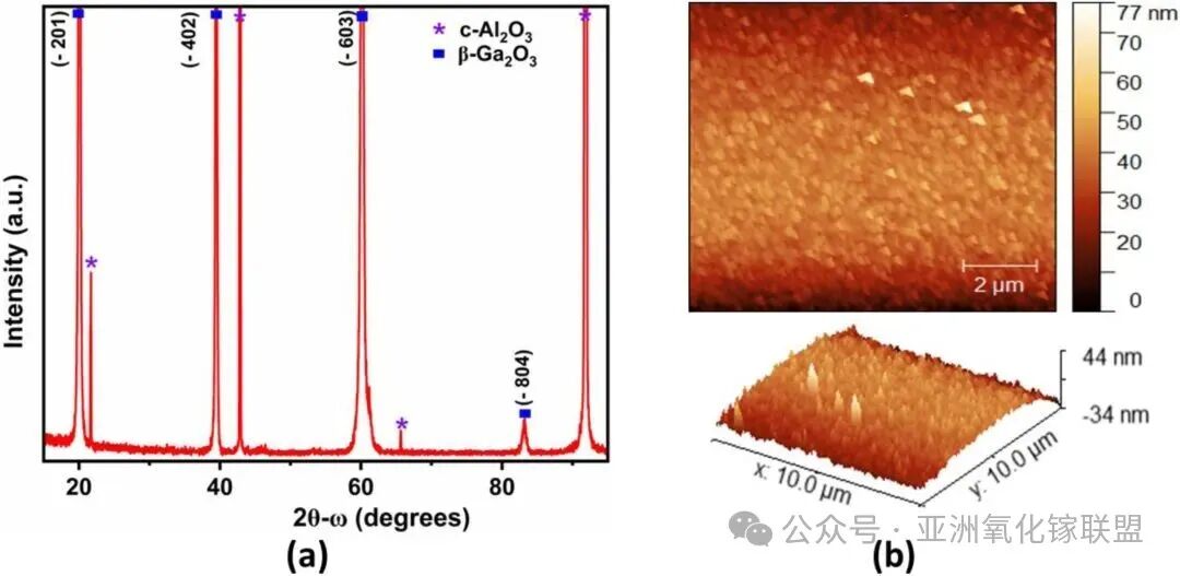
Figure 1.(a) XRD 2θ−ω scan pattern of β-Ga₂O₃ thin films grown on c-sapphire substrates at a growth temperature of 650 °C;(b) 2D and 3D AFM images showing the surface roughness of β-Ga₂O₃ thin films grown by the PLD method.
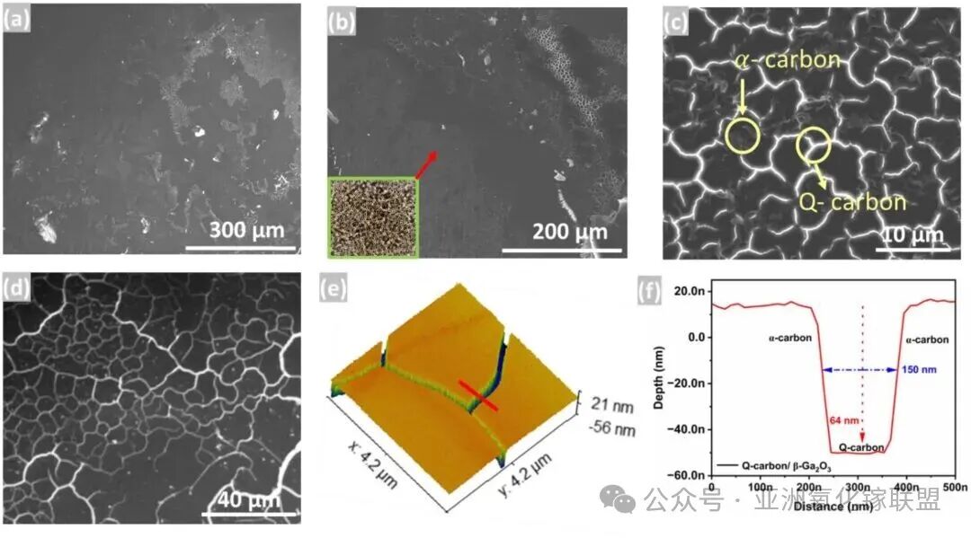
Figure 2.(a) Scanning electron microscopy (SEM) image showing the formation of large-area Q-carbon on the β-Ga₂O₃ surface after PLA treatment;(b) Formation of Q-carbon fibrous structures, with early-stage Q-carbon regions observed along the sidewalls;(c) High-magnification image of Q-carbon fibrous structures surrounded by dark α-carbon regions;(d) Different crack widths observed within regions exposed to the same PLA energy density;(e) AFM image showing the height difference between Q-carbon and α-carbon regions on the film surface;(f) Line profile and depth profile indicating thickness variations between the Q-carbon and α-carbon phases.
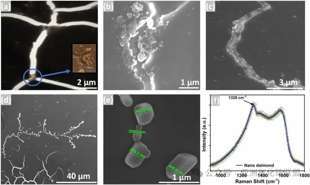
Figure 3.(a) SEM image of the laser-irradiated region, showing the contraction of Q-carbon and nanodiamond structures;(b) Fibers beginning to fracture after multiple laser irradiations;(c) SEM image taken at a 52° tilt angle, showing the formation of nanodiamonds across the entire fibrous region;(d) & (e) Tilted-view SEM images (52°) of the overall diamond structure at different magnifications, along with top-view images of nanodiamonds ranging in size from 200 nm to 500 nm;(f) Raman spectrum of the irradiated region, where the nanodiamond peak appears at 1320 cm⁻¹. Due to the presence of amorphous carbon in the surrounding areas, prominent D and G peaks are also observed.
