Paper Sharing
【Domestic Papers】High-Performance BDD/Ga₂O₃ Heterojunction Temperature Sensor with Enhanced Sensitivity, Wide Temperature Range, and Robust Anti-Interference Capabilities
日期:2026-05-20阅读:157
Researchers from the Shandong University & Beijing University of Posts and Telecommunications have published a dissertation titled "High-Performance BDD/Ga₂O₃ Heterojunction Temperature Sensor with Enhanced Sensitivity, Wide Temperature Range, and Robust Anti-Interference Capabilities" in Journal of Alloys and Compounds.
Background
Wide-bandgap semiconductor materials (e.g., BDD, Ga₂O₃) feature an ultra-wide bandgap, high stability, and strong radiation resistance, making them ideal candidates for electronic devices in extreme environments. Conventional temperature sensors generally suffer from low sensitivity, limited operating temperature range, and susceptibility to optical interference, failing to meet the stringent requirements for high-precision and highly stable temperature measurement in aerospace, military, and medical fields. Heterojunction structures can regulate carrier transport properties via bandgap engineering, offering an effective approach to address the aforementioned bottlenecks. Therefore, a novel temperature sensor with high sensitivity, a wide operating temperature range, and strong anti-interference capability is urgently needed.
Abstract
We report here a high-performance boron-doped diamond (BDD)/gallium oxide (Ga₂O₃) heterojunction temperature sensor with superior sensitivity in a wide operational temperature range. The sensor was fabricated in a two-step process: first, a BDD layer was grown on a commercial (100) diamond substrate via microwave plasma chemical vapor deposition (MPCVD), followed by the deposition of a Ga₂O₃ film using magnetron sputtering.The temperature dependent electrical performance of the sensor was evaluated through current-voltage (I-V) measurements at elevated temperatures, which revealed a clear negative shift of the turn-on voltages as the temperature increased, attributed to enhanced carrier diffusion and thermal excitation. The sensor achieves a remarkable sensitivity of up to 6.24 mV/K (at 100 mA) over a wide temperature range of 300–550 K, which outperforms other semiconductor temperature sensors made from materials such as silicon (Si), gallium nitride (GaN), and oxide-based compounds due to the ultra-wide bandgap of BDD and Ga₂O₃.The sensor also exhibits excellent reliability and minimal sensitivity fluctuations after storage for 312 days and under optical exposure to 455 and 532 nm lasers. The BDD/Ga₂O₃ heterojunction sensor is ideal for applications that require precise thermal response and reliability in dynamic environments, such as aerospace, military, and medical systems.
Highlights
The first BDD/β-Ga₂O₃ p-n heterojunction temperature sensor with ultrawide bandgaps achieves a record sensitivity of 6.24 mV/K at 100 mA over the temperature range of 300–550 K.
Sensitivity surpasses conventional Si/GaN/oxide sensors (2–4.5 mV/K) due to Type-II staggered alignment and enhanced barrier modulation.
Exceptional stability: no measurable drift after 312 days of ambient storage or prolonged exposure to 455/532 nm lasers (0.8 mW/cm²).
Scalable fabrication via MPCVD + magnetron sputtering enables integration into harsh-environment sensing platforms.
Conclusion
In summary, we demonstrate in this study a high-performance temperature sensor based on a BDD/Ga₂O₃ heterojunction. The sensor was fabricated in two sequential steps: MPCVD growth of a BDD layer on a commercial diamond substrate, followed by deposition of a thin Ga₂O₃ film. The device performance was evaluated at elevated temperatures and the results demonstrate that the sensor exhibits a high temperature sensitivity. The BDD/Ga₂O₃ heterojunction sensor demonstrates a maximum temperature sensitivity of 6.24 mV/K at 100 mA.We attribute the enhanced performance to the ultrawide bandgaps, intrinsic chemical inertness, and physical robustness of BDD and Ga₂O₃. Further experiments reveal that the sensor has excellent minimal sensitivity drift after 312 days of storage and under laser exposures. We believe that the BDD/Ga₂O₃ heterojunction temperature sensor offers a promising solution for applications demanding precise and stable thermal monitoring in dynamic environments, including aerospace, defense, and medical systems.
Project Support
This work was supported by the National Science Foundation of China (NSFC, Grant No. 52172296), Jinan Branch, Hefei National Laboratory, and the Initiative in Quantum Science of Shandong Provincial Natural Science Foundation (ZR2020LLZ005).
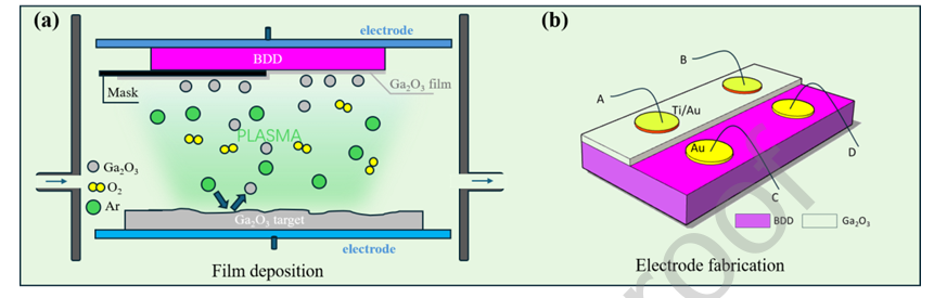
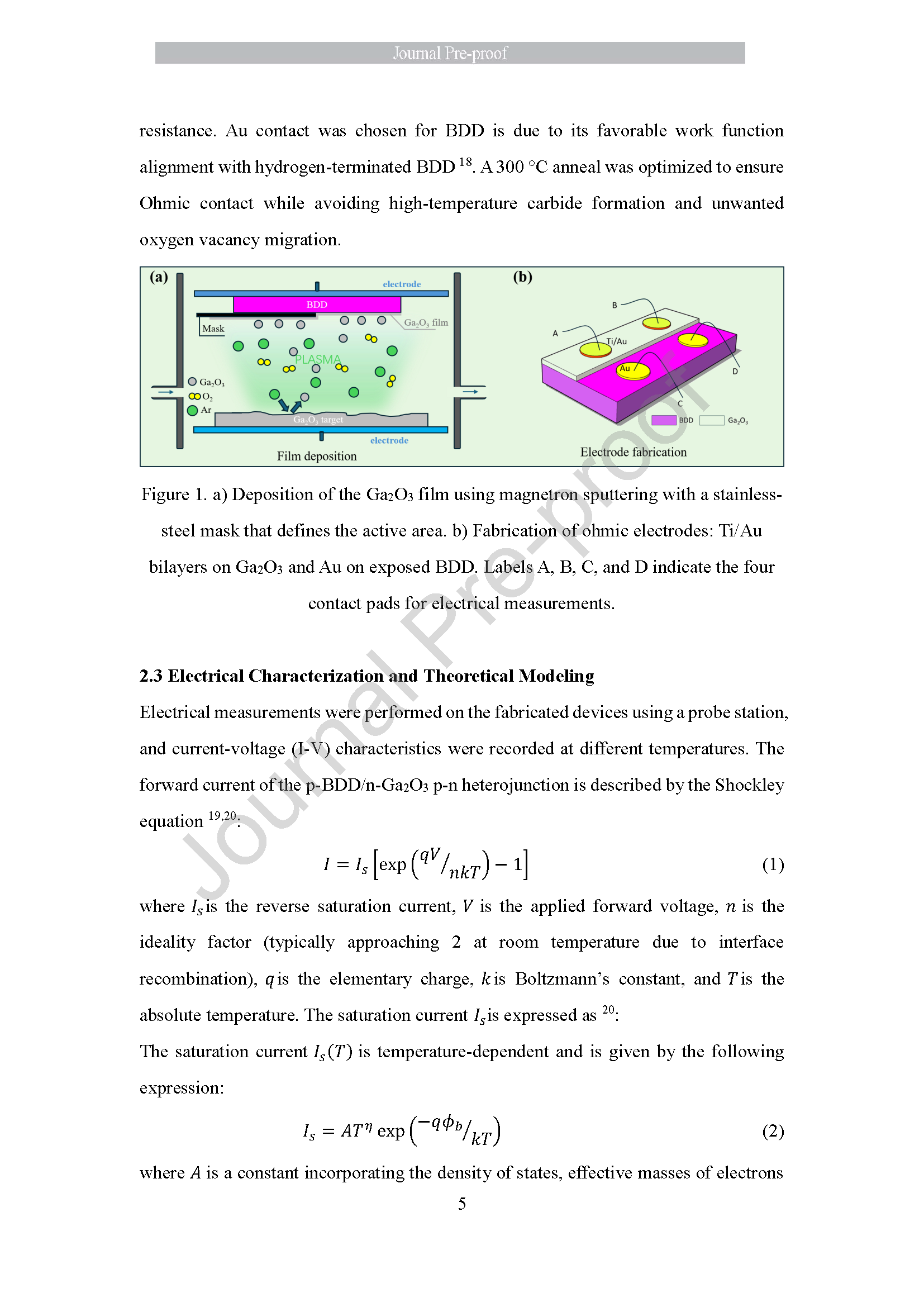
Figure 1 a) Deposition of the Ga₂O₃ film using magnetron sputtering with a stainlesssteel mask that defines the active area. b) Fabrication of ohmic electrodes: Ti/Au contact pads bilayers on Ga₂O₃ and Au on exposed BDD. Labels A, B, C, and D indicate the four contact pads for electrical measurements.
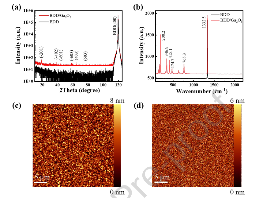
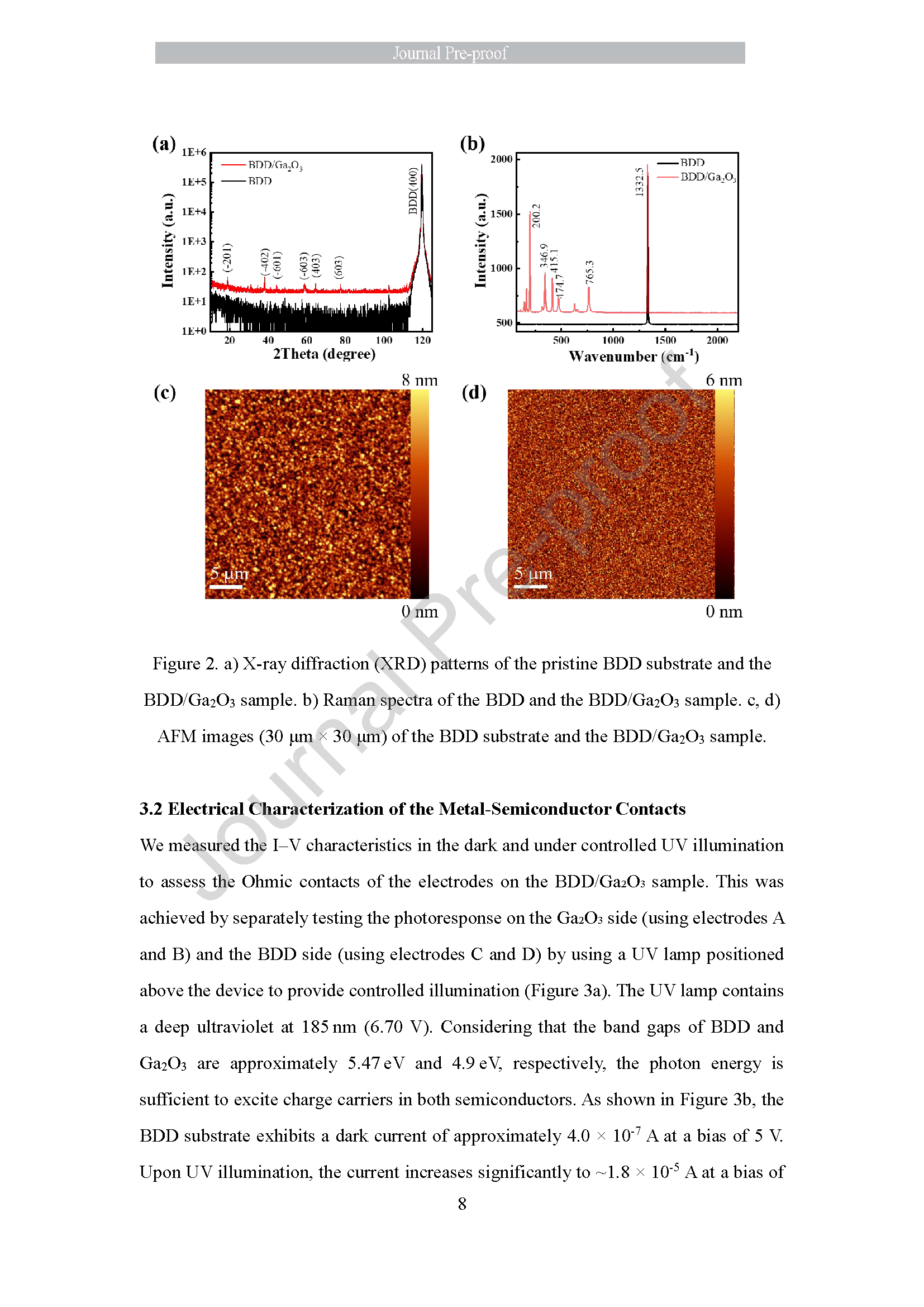
Figure 2 a) X-ray diffraction (XRD) patterns of the pristine BDD substrate and the BDD/Ga₂O₃ sample. b) Raman spectra of the BDD and the BDD/Ga₂O₃ sample. c, d) AFM images (30 μm × 30 μm) of the BDD substrate and the BDD/Ga₂O₃ sample.
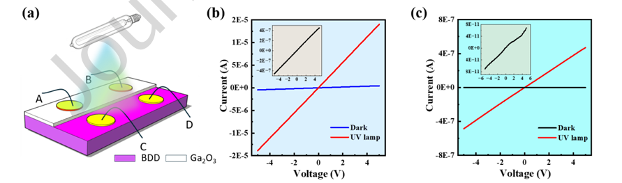
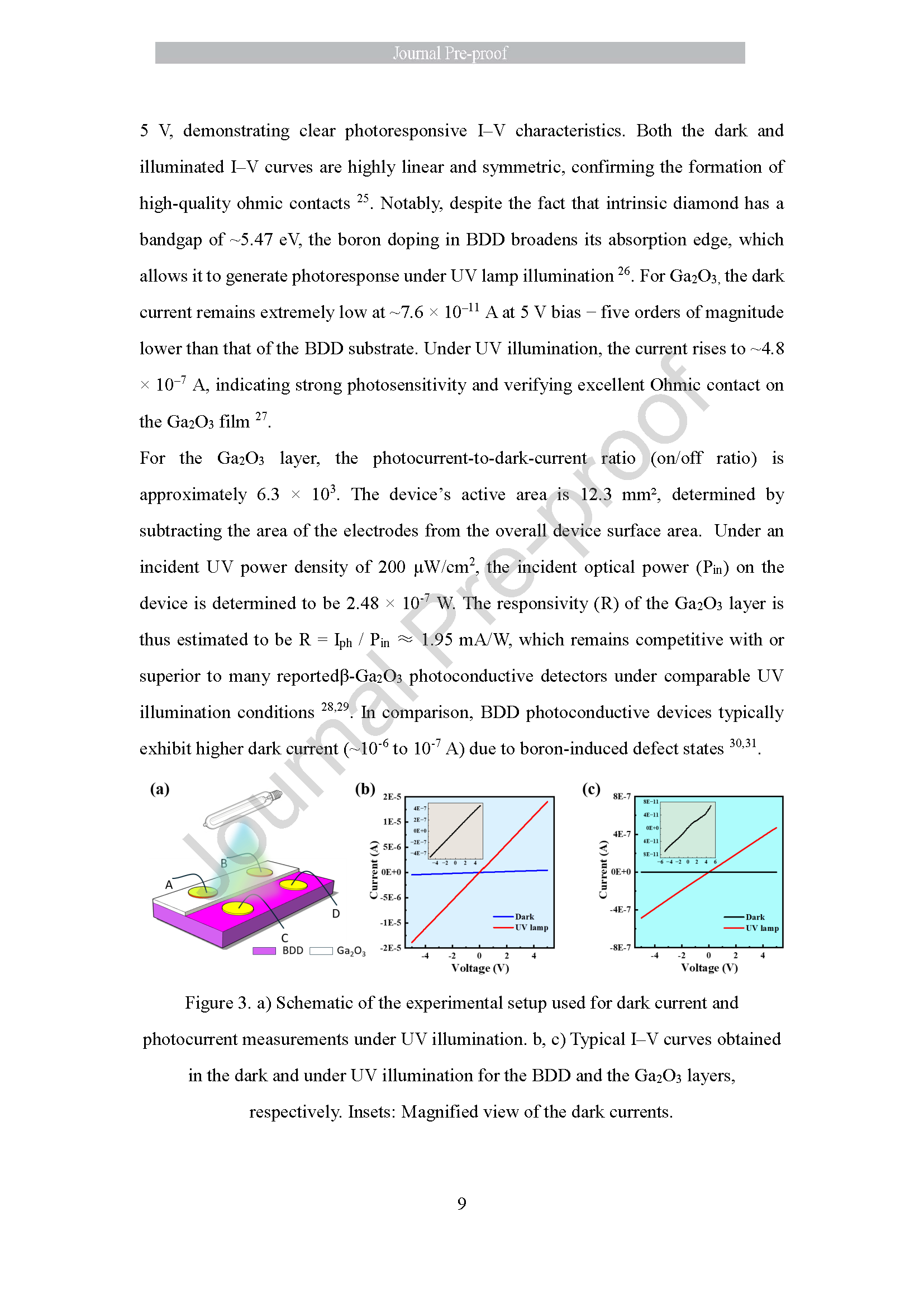
Figure 3 a) Schematic of the experimental setup used for dark current and photocurrent measurements under UV illumination. b, c) Typical I–V curves obtained in the dark and under UV illumination for the BDD and the Ga₂O₃ layers, respectively. Insets: Magnified view of the dark currents.
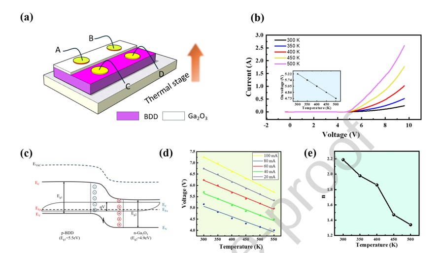
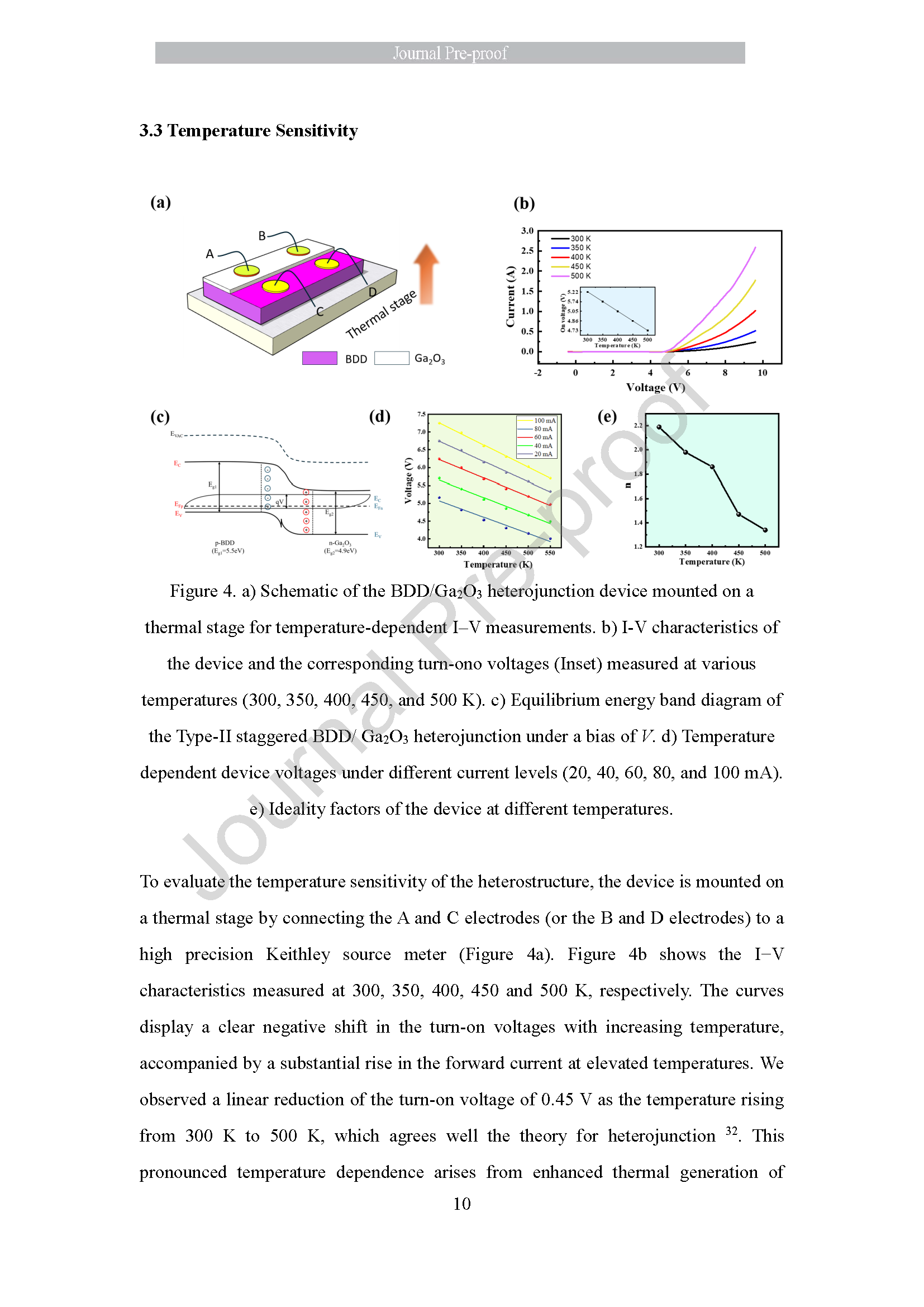
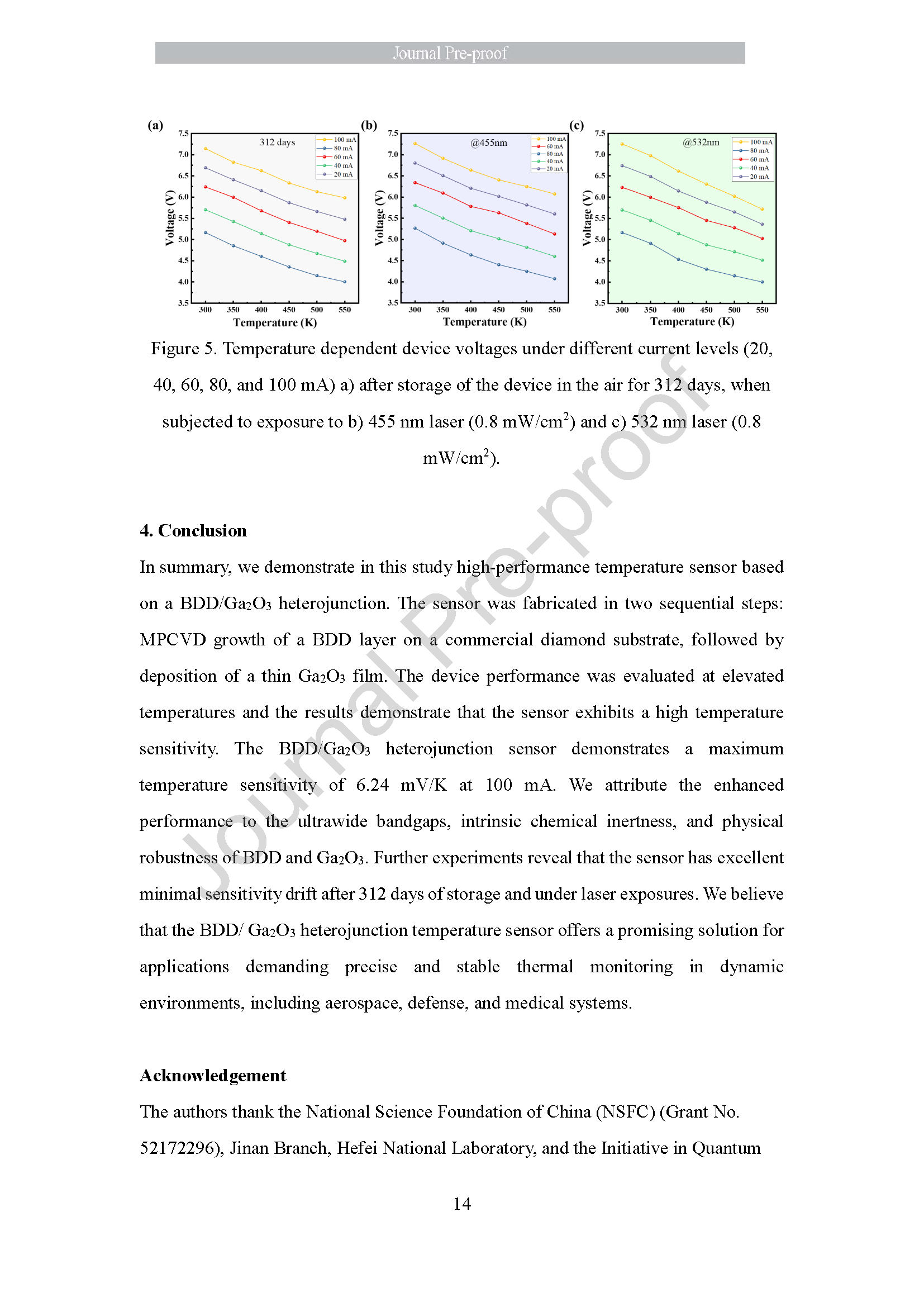
Figure 4 a) Schematic of the BDD/Ga₂O₃ heterojunction device mounted on a thermal stage for temperature-dependent I–V measurements. b) I-V characteristics of the device and the corresponding BDD/Ga₂O₃ turn-on voltages (Inset) measured at various temperatures (300, 350, 400, 450, and 500 K). c) Equilibrium energy band diagram of the Type-II staggered BDD/Ga₂O₃ heterojunction under a bias of V. d) Temperature dependent device voltages under different current levels (20, 40, 60, 80, and 100 mA). e) Ideality factor of the device at different temperatures.
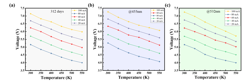
Figure 5 Temperature dependent device voltages under different current levels (20, 40, 60, 80, and 100 mA) a) after storage of the device in the air for 312 days, when subjected to exposure to b) 455 nm laser (0.8 mW/cm²) and c) 532 nm laser (0.8 mW/cm²).
DOI:
doi.org/10.1016/j.jallcom.2026.188576