Paper Sharing
【International Papers】MOCVD Growth of κ-Ga₂O₃ on Al-Rich AlₓGa₁₋ₓN Templates: Phase Diagram and Microstructural Evolution
日期:2026-05-21阅读:25
Researchers from the University of Bristol and the University of Cambridge have published a dissertation titled “MOCVD Growth of κ-Ga₂O₃ on Al-Rich AlₓGa₁₋ₓN Templates: Phase Diagram and Microstructural Evolution” in Crystal Growth & Design.
Background
κ-Ga₂O₃, as a metastable wide-bandgap material with strong spontaneous polarization, can form high-mobility two-dimensional electron gases in heterostructures and shows great potential in next-generation power devices. However, its epitaxial growth tends to form stable β-phase, degrading polarization properties. Conventional sapphire substrates easily introduce defects such as rotational domains, and the growth window of κ-phase is narrow. At present, there is still a lack of systematic research on the MOCVD growth window, phase competition, and microstructural evolution at ultra-thin layer stages of κ-Ga₂O₃ on Al-rich AlₓGa₁₋ₓN templates, and the growth mechanism remains unclear.
Abstract
Orthorhombic k-phase Ga₂O₃ is a metastable, ferroelectric polymorph of Ga₂O₃ with a large spontaneous polarization, offering a pathway to polarization-induced high-mobility 2D electron gases via κ-Ga₂O₃/AlₓGa₁₋ₓN heterostructures. Here, we map the metal−organic chemical vapor deposition (MOCVD) growth window of κ-Ga₂O₃ on Al-rich AlₓGa₁₋ₓN-on-sapphire template layers (x = 0.5 and 0.75) by systematically varying the gallium and oxygen precursor flow rates and benchmark these results against cogrown films on c-plane sapphire. On Al0.5Ga0.5N, κ-Ga₂O₃ can be grown over a wide range of conditions extending to low growth rates and high VI/III regions, whereas on sapphire substrates the k-phase favorable window is restricted to the high growth rate and low VI/III regime only. Microstructural and phase evolution analyses by X-ray diffraction (XRD) and transmission electron microscopy (TEM) of the κ-Ga₂O₃ films grown on Al0.5Ga0.5N confirms that growth initiates as a phase-pure monoclinic β-Ga₂O₃ layer; κ-Ga₂O₃ nucleation starts between 20 and 45 nm of layer thickness and becomes the only phase growing around ∼100−250 nm thick, resulting in a phase-pure κ-Ga₂O₃ top surface. A similar progression was observed for growth on x = 0.75 AlₓGa₁₋ₓN template layers.
Highlights
The MOCVD growth phase diagram of κ-Ga₂O₃ on Al-rich AlₓGa₁₋ₓN templates (x = 0.5, 0.75) is established for the first time.
κ-Ga₂O₃ exhibits a much wider growth window on AlₓGa₁₋ₓN than on c-plane sapphire.
A three-stage phase evolution mechanism from pure β-Ga₂O₃ to phase-pure κ-Ga₂O₃ is revealed.
κ-Ga₂O₃ nucleates later at 20–45 nm and dominates after 100–250 nm thickness.
The growth mechanism is consistent for both Al0.5Ga0.5N and Al0.75Ga0.25N templates.
Conclusion
We show that κ-Ga₂O₃ growth on Al-rich Al0.5Ga0.5N template layers by MOCVD is favored across a broad range of growth rates and VI/III ratios, unlike on c-plane sapphire where the κ-Ga₂O₃ favorable window is specifically constrained to high growth rate and low VI/III ratios only. Analysis of the structural evolution of the Ga₂O₃ films on Al0.5Ga0.5N template layers under κ-Ga₂O₃ favorable conditions reveals three main stages. In the first stage, the β-Ga₂O₃ transition layer invariably forms, then, κ-Ga₂O₃ starts nucleating on the β-Ga₂O₃ transition layer at some point between 20 and 45 nm of layer thickness. This marks the start of the stage, during which grains of both polymorphs grow simultaneously. Eventually, growth enters the third stage when κ-Ga₂O₃ grains have coalesced and completely covered over β-grains, blocking the latter’s growth. This was seen to occur between 100 and 250 nm of layer thickness. Only κ-Ga₂O₃ grows in this stage, resulting in a phase-pure κ-Ga₂O₃ top surface. Overall, it appears that this growth mode on Al-rich AlₓGa₁₋ₓN templates is largely consistent with that reported for GaN at the low Al composition limit.
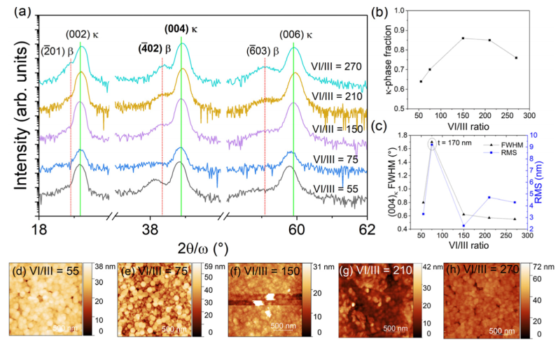
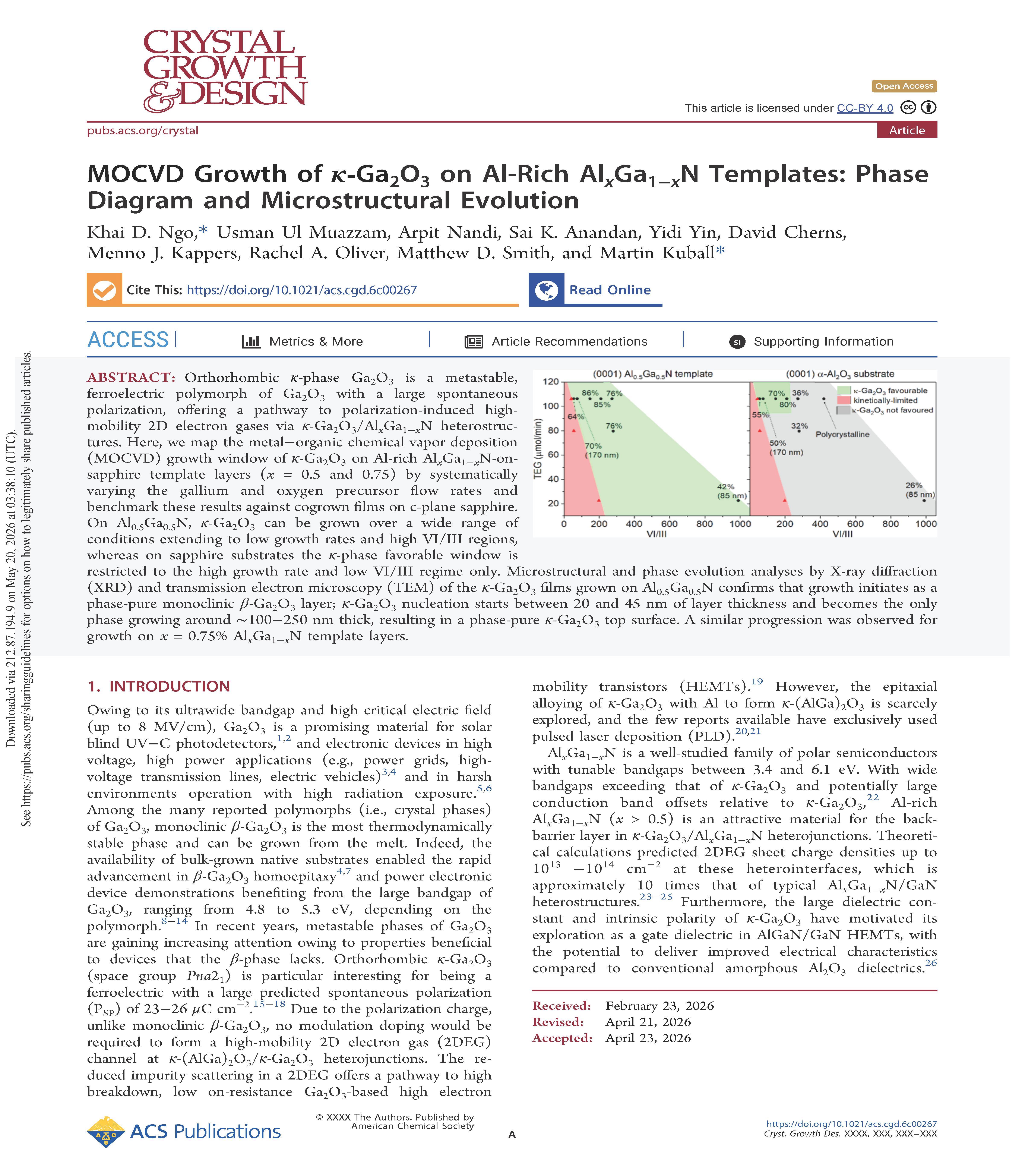
Figure 1. Structural characterization of Ga₂O₃ films grown on Al0.5Ga0.5N templates for VI/III ratios between 55 and 270 (constant TEGa = 106 μmol/min, Tgr = 500 °C, pT = 10 Torr): (a) XRD 2θ-ω scans showing the {-201}β and {002}κ reflections; (b) κ-phase fraction (estimated using (-402)β and (004)κ peak intensities) against VI/III ratio; (c) XRC fwhm of the (004)κ reflection and surface root-mean-square (RMS) roughness against VI/III ratio. AFM scans of a 2 × 2 μm² area of the films for VI/III = (d) 55, (e) 75, (f) 150, (g) 210, (h) 270.
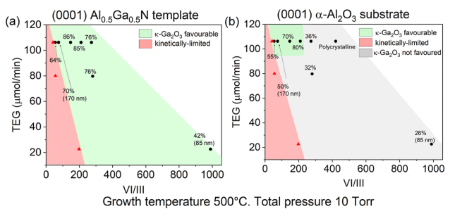
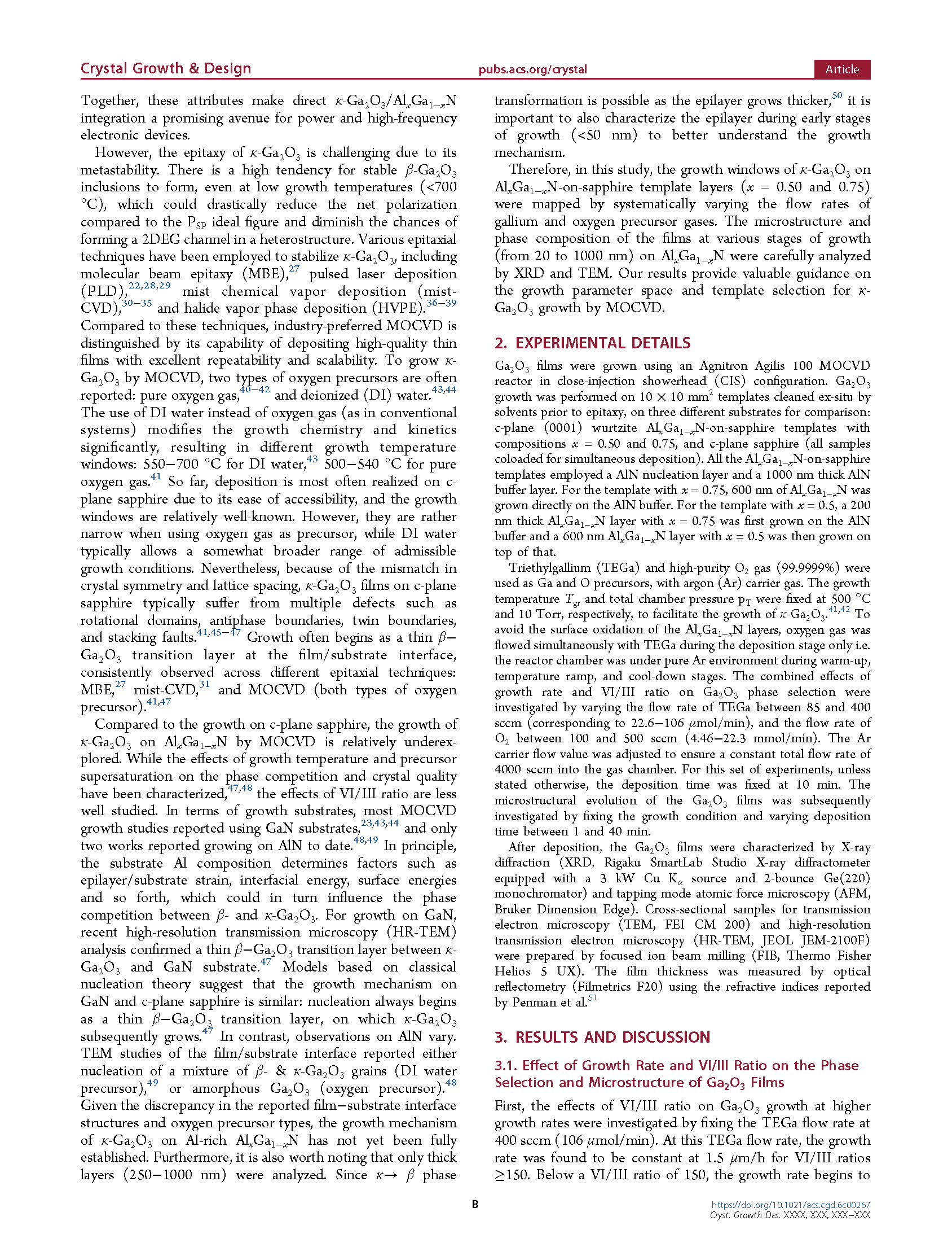
Figure 2. Growth phase diagram of Ga₂O₃ on (a) (0001) Al0.5Ga0.5N and (b) c-plane sapphire (Tgr = 500 °C, pT = 10 Torr held constant). Regions shaded in red correspond to kinetically limited growth conditions, which would result in no epitaxial growth because of insufficient oxidation. Regions shaded in green correspond to κ-Ga₂O₃ favorable growth conditions, which would result in films with κ-phase fraction ≥50% at 200 nm thick. Gray regions indicate conditions where κ-Ga₂O₃ is not favored. Note that the shaded regions serve only as guides to the eye, and boundaries between them are approximate. Unshaded regions (in white) correspond to unexplored conditions.
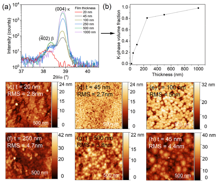
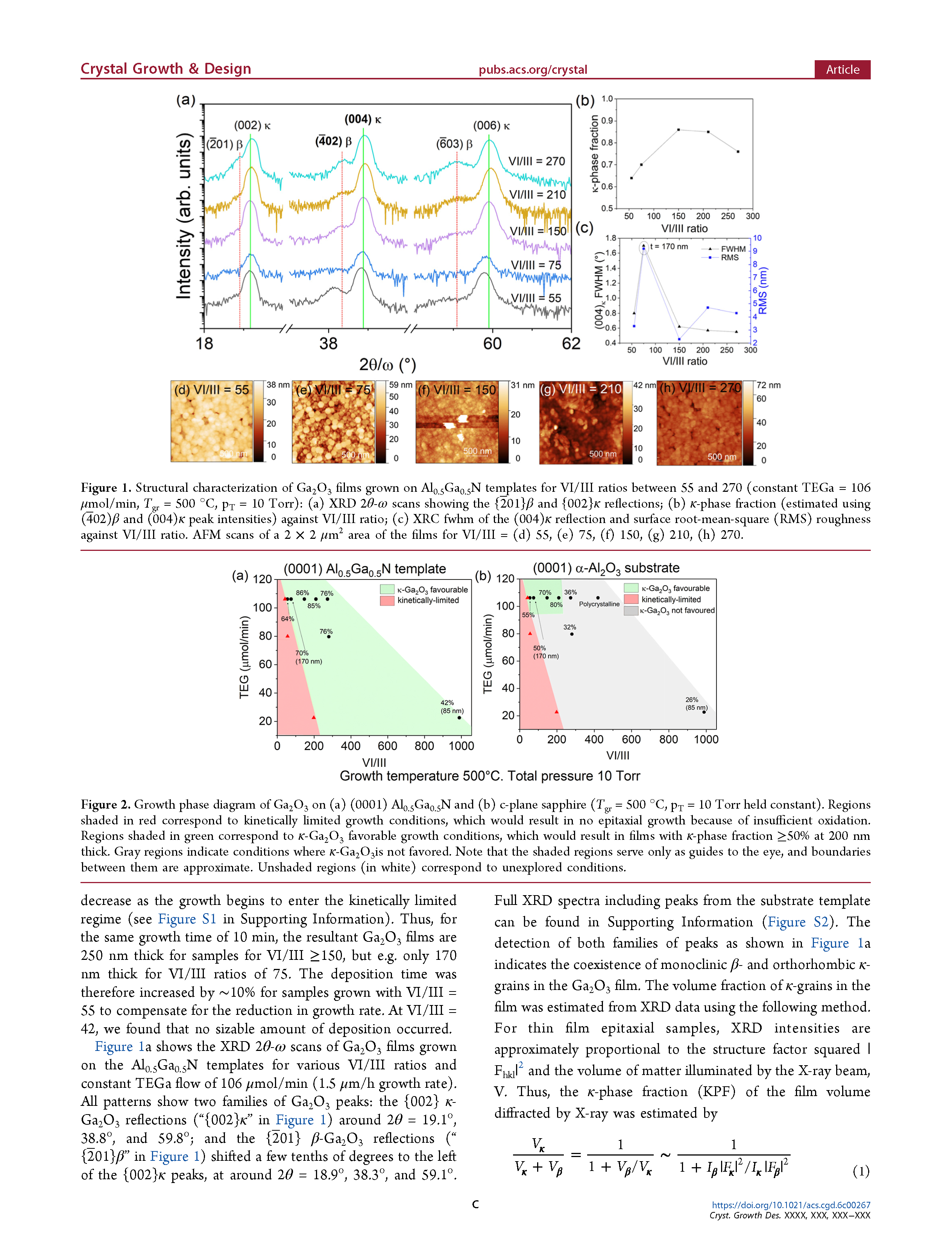
Figure 3. (a) XRD 2θ-ω scans, (b) κ-phase fraction, (c−h) AFM scans of Ga₂O₃ films 20−1000 nm thick grown on Al0.5Ga0.5N templates, under identical growth conditions (TEG = 106 μmol/min, VI/III = 210, Tgr = 500 °C, pT = 10 Torr).
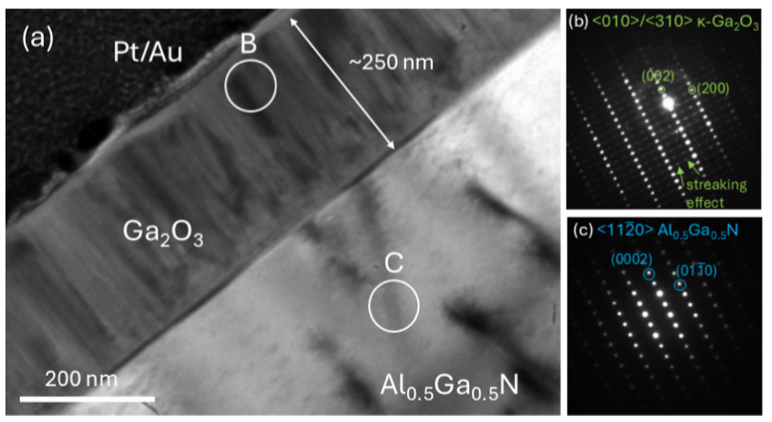
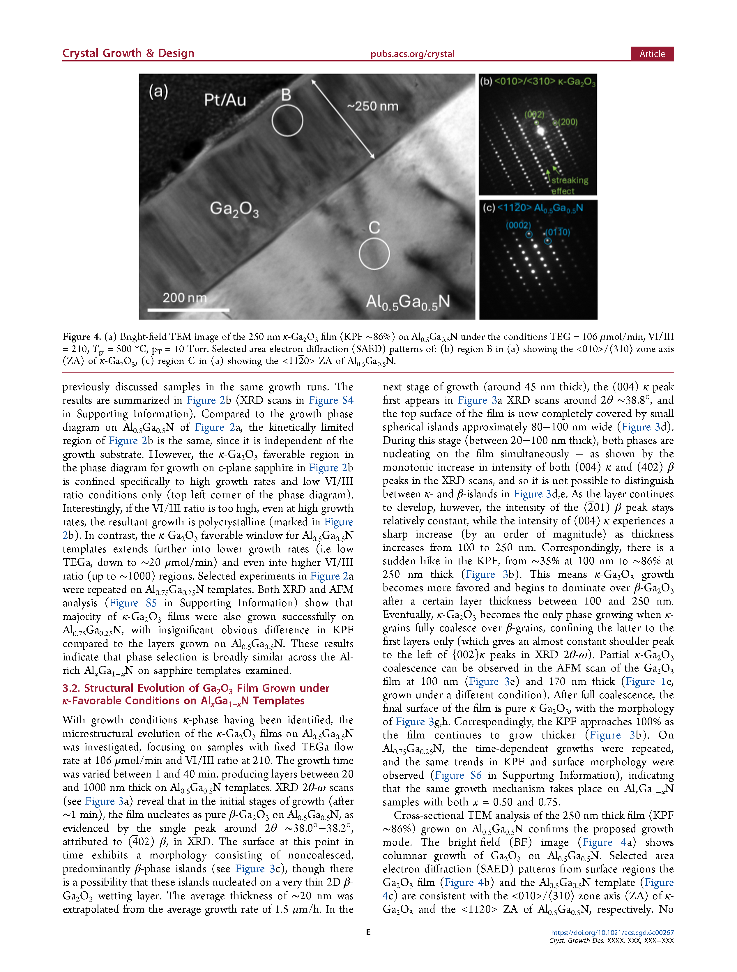
Figure 4. (a) Bright-field TEM image of the 250 nm κ-Ga₂O₃ film (KPF ∼86%) on Al0.5Ga0.5N under the conditions TEG = 106 μmol/min, VI/III = 210, Tgr = 500 °C, pT = 10 Torr. Selected area electron diffraction (SAED) patterns of: (b) region B in (a) showing the <010>/⟨310⟩ zone axis (ZA) of κ-Ga₂O₃, (c) region C in (a) showing the <11-20> ZA of Al0.5Ga0.5N.
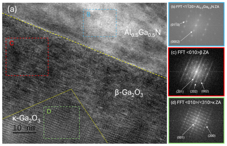
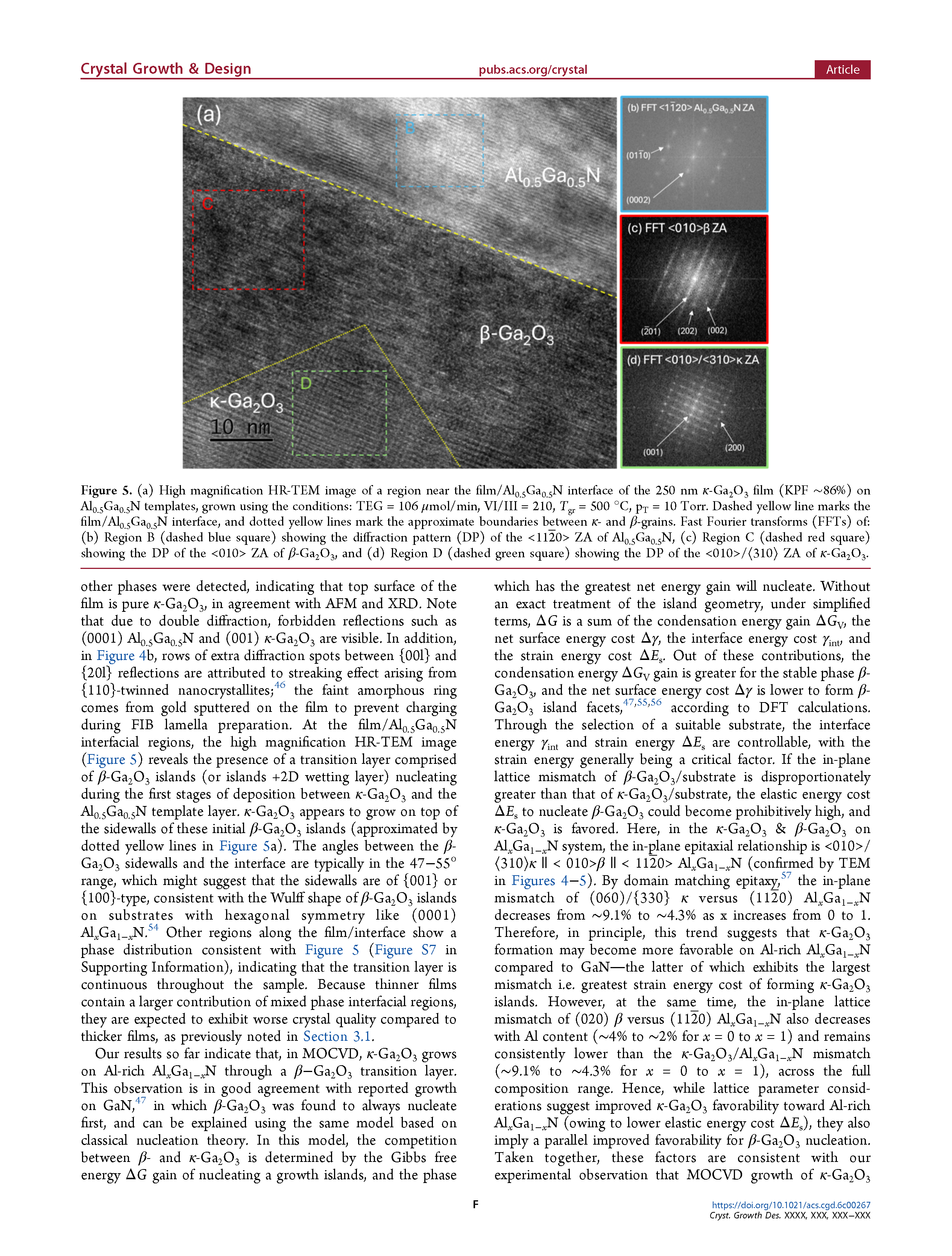
Figure 5. (a) High magnification HR-TEM image of a region near the film/Al0.5Ga0.5N interface of the 250 nm κ-Ga₂O₃ film (KPF ∼86%) on Al0.5Ga0.5N templates, grown using the conditions: TEG = 106 μmol/min, VI/III = 210, Tgr = 500 °C, pT = 10 Torr. Dashed yellow line marks the film/Al0.5Ga0.5N interface, and dotted yellow lines mark the approximate boundaries between κ- and β-grains. Fast Fourier transforms (FFTs) of: (b) Region B (dashed blue square) showing the diffraction pattern (DP) of the <11-20> ZA of Al0.5Ga0.5N, (c) Region C (dashed red square) showing the DP of the <010> ZA of β-Ga₂O₃, and (d) Region D (dashed green square) showing the DP of the <010>/⟨310⟩ ZA of κ-Ga₂O₃.
DOI:
doi.org/10.1021/acs.cgd.6c00267