Paper Sharing
【Member Papers】Trap-Induced Instability in β Ga₂O₃ Solar-Blind Phototransistors Under Electro-Optical Stress
日期:2026-05-22阅读:15
Researchers from Xidian University have published a dissertation titled “Trap-Induced Instability in β‑Ga₂O₃ Solar-Blind Phototransistors Under Electro-Optical Stress” in IEEE TRANSACTIONS ON ELECTRON DEVICES.
Background
β‑Ga₂O₃ solar-blind phototransistors are of great value in ultraviolet communication, flame detection, and space imaging due to their ultra-wide bandgap and high gain. However, under long-term electro-optical coupling stress, devices suffer from reliability issues such as threshold voltage shift, pinch-off current degradation, and detectivity attenuation, which severely restrict their long-term stable operation. Most existing studies focus on interface trap behavior, while the synergistic mechanism of buffer layer bulk traps, photo-assisted trap activation, and electric field is still unclear. There is a lack of systematic explanation and physical model for the origin of device instability under the combined action of negative bias stress and ultraviolet illumination.
Abstract
The trap-assisted instability in β‑Ga₂O₃ solar-blind phototransistors under long-term electro-optical stress is systematically investigated. Under the negative bias stress (NBS) in the dark, threshold voltage (Vth) first shifts slightly negative at −3 V and then positive to 0.05 V at −5 V, accompanied by a reduced hysteresis (ΔVhysteresis). This transition is attributed to a crossover from border-trap-dominated detrapping to field-assisted capture by bulk traps in the β‑Ga₂O₃ buffer layer. Although the responsivity (R) remains nearly constant, detectivity (D*) decreases by almost one order of magnitude due to leakage-induced enhancement of the pinch-off current (Ipinch-off). Under simultaneous ultraviolet (UV) illumination, the Vth shift enlarges to 0.3 V, and the Ipinch-off degradation ratio increases from 136% to 298%, indicating strong photoassisted charge buildup in the buffer. In this regime, both R and D* degrade by nearly an order of magnitude as photo-generated carriers activate abundant deep traps and accelerate electron capture. A trap-assisted physical model incorporating border and buffer traps reproduces the observed parameter shifts and current degradation. These results reveal that photo-induced activation of buffer-layer traps is the primary origin of electro-optical instability, highlighting buffer-layer defect engineering as a key route to enhance the long-term reliability of β‑Ga₂O₃ solar-blind phototransistors.
Highlights
Systematically investigate the trap-induced instability of β‑Ga₂O₃ solar-blind phototransistors under long-term electro-optical stress.
Clarify the transition mechanism from border trap detrapping to bulk trap capture under negative bias stress.
Reveal that photo-assisted activation of buffer layer traps dominates the electro-optical instability.
Establish a trap-assisted physical model to explain threshold voltage shift and current degradation.
Propose buffer layer defect engineering to improve the long-term reliability of devices.
Conclusion
In summary, the Vth evolution from −0.1 to +0.05 V and the increase in Ipinch-off degradation from 42% to 84% indicate that instability under NBS arises from electron detrapping at border traps together with electron trapping in buffer-layer defects. Under NBIS, the larger positive Vth shift of 0.3 V and the escalation in Ipinch-off degradation from 136% to 298% show that photo-assisted trapping in the UID buffer layer becomes the dominant mechanism, accelerating parameter drift. These results confirm that UV illumination not only enhances electron capture but also activates trap states that are electrically inactive in the dark, effectively increasing the density of accessible deep traps and strengthening charge buildup. The analysis provides a consistent photograph of the electro-optical degradation process and highlights the need to suppress trap density in the UID buffer layer to improve the long-term stability of β‑Ga₂O₃ solar-blind phototransistors.
Project Support
This work was supported in part by the National Natural Science Foundation of China under Grant 62404176 and Grant 62293522, in part by the National Key Research and Development Program of China under Grant 2024YFF1504400, in part by the Zhejiang Provincial Natural Science Foundation of China under Grant LDT23F0402 and Grant LDT23F04024F04, and in part by the Leading Innovation and Entrepreneurship Project of Zhejiang Province under Grant 2023R01014.
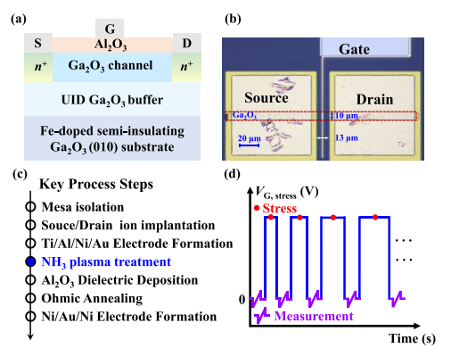
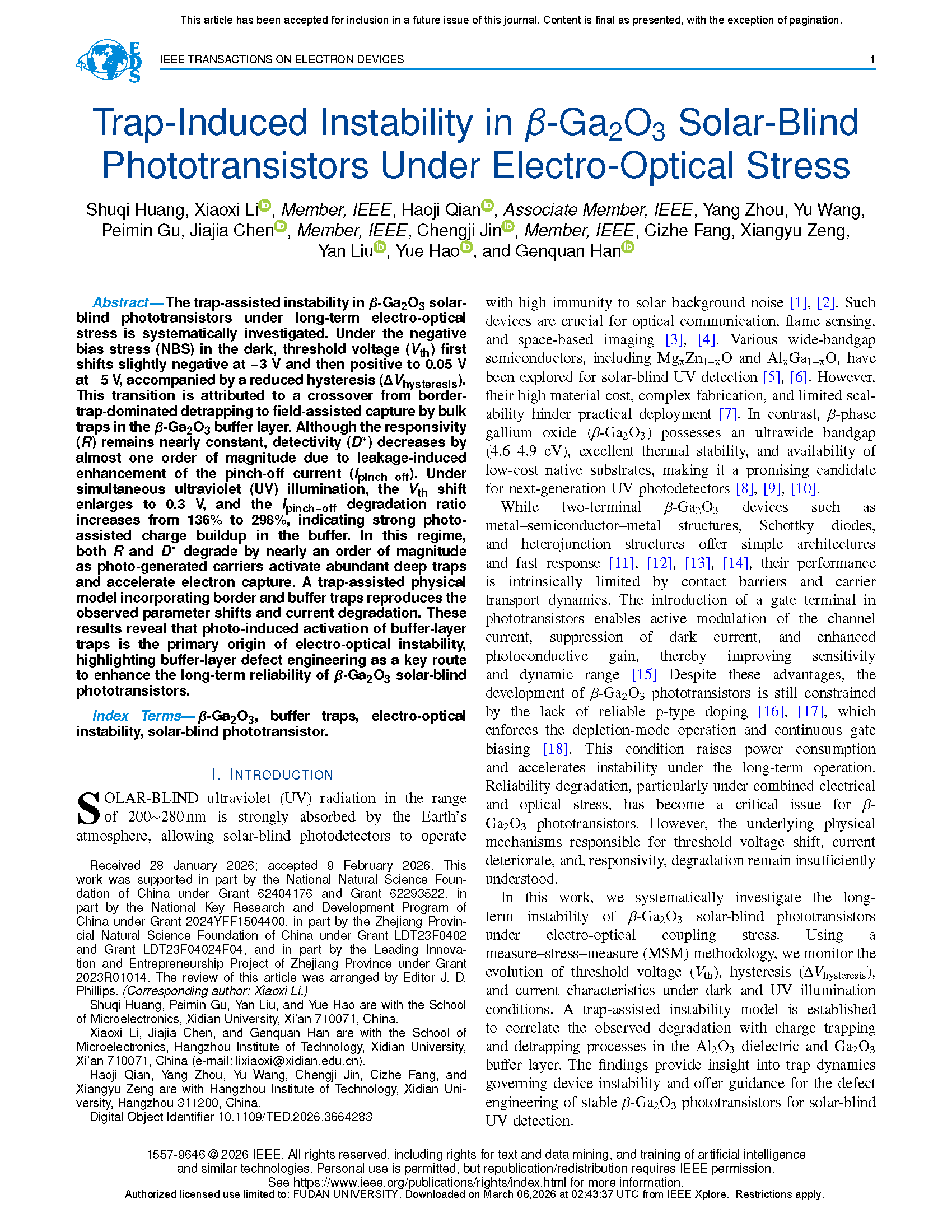
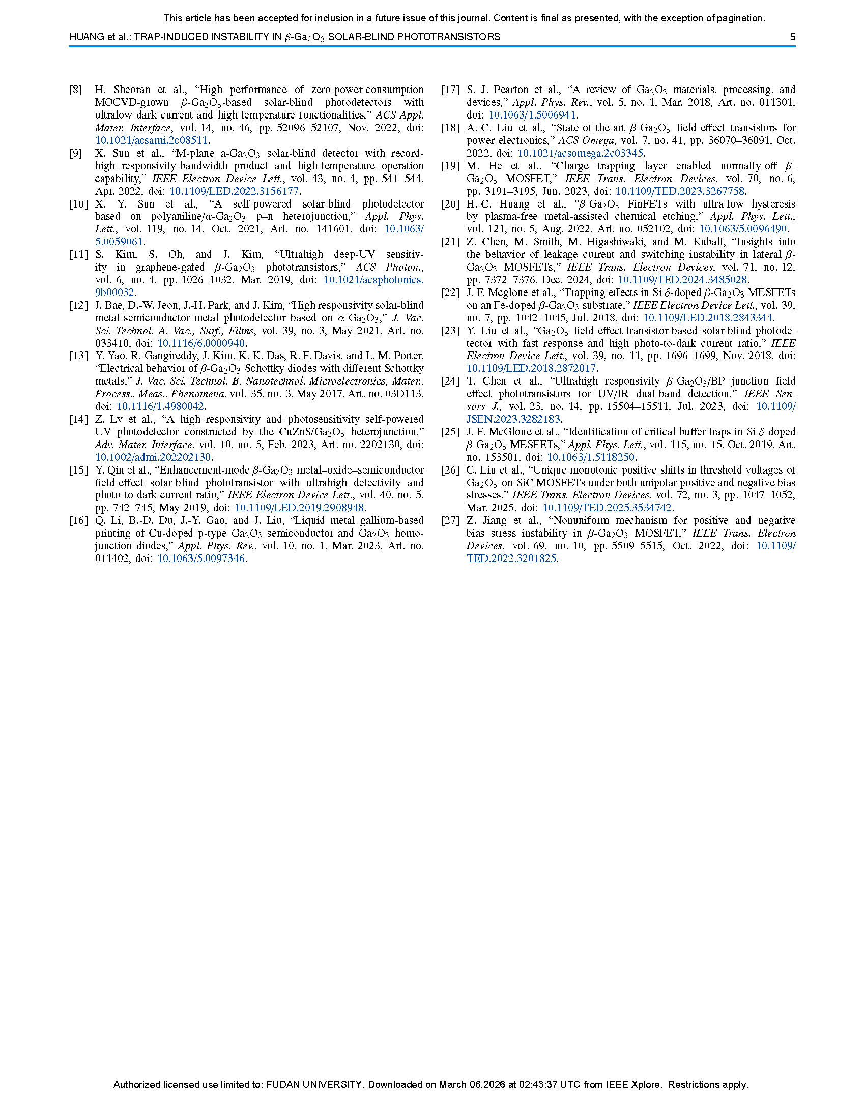
Fig. 1. (a) Schematic of the cross-sectional view. (b) Optical microscope image. (c) Key process steps of the fabricated device. (d) MSM scheme for stress tests.
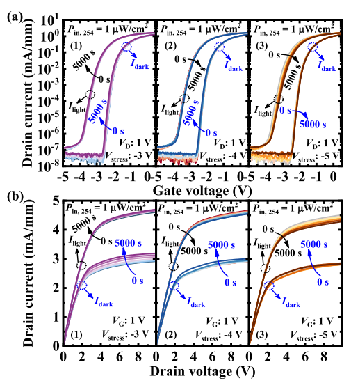
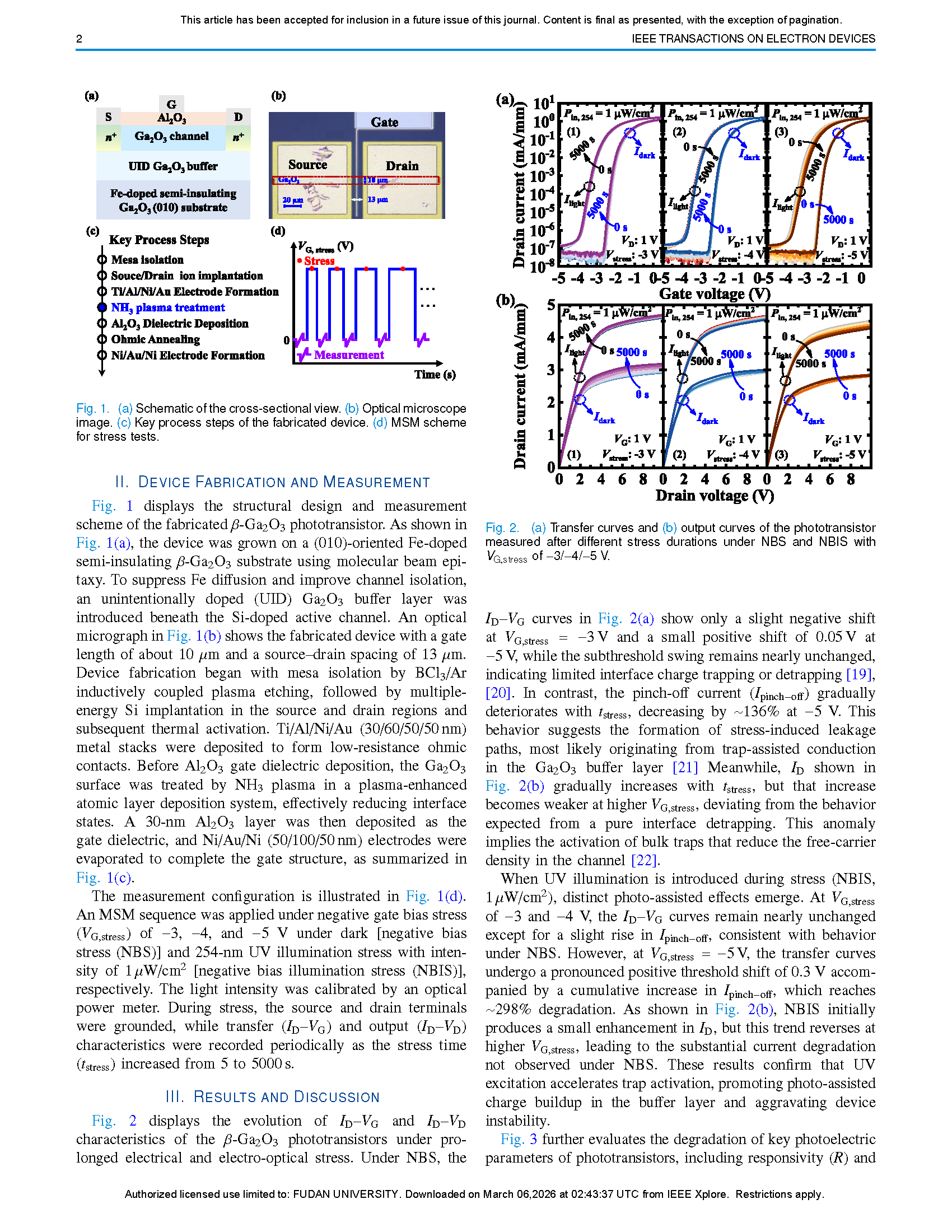
Fig. 2. (a) Transfer curves and (b) output curves of the phototransistor measured after different stress durations under NBS and NBIS with VG,stress of −3/−4/−5 V.
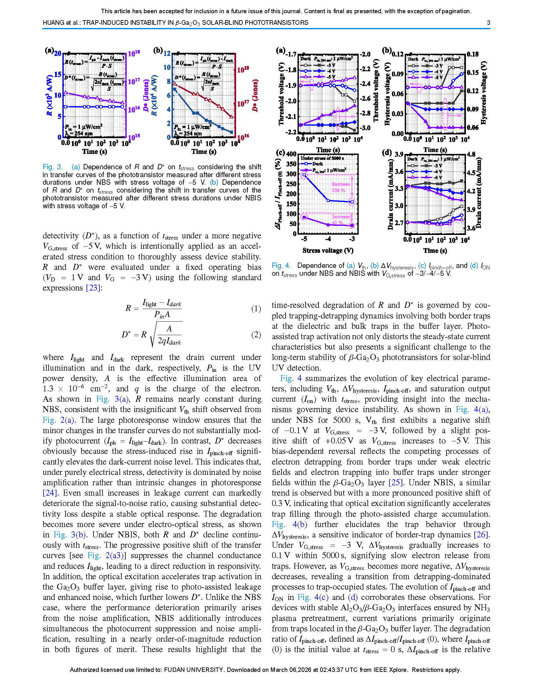
Fig. 3. (a) Dependence of R and D∗ on tstress considering the shift in transfer curves of the phototransistor measured after different stress durations under NBS with stress voltage of −5 V. (b) Dependence of R and D* on tstress considering the shift in transfer curves of the phototransistor measured after different stress durations under NBIS with stress voltage of −5 V.
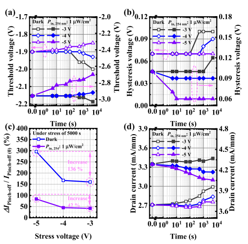
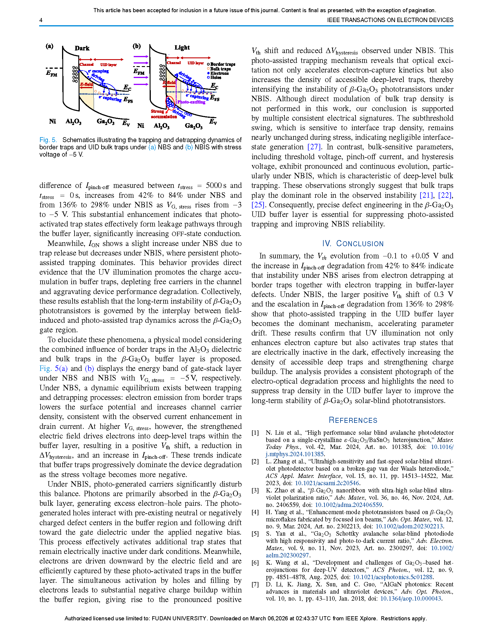
Fig. 4. Dependence of (a) Vth, (b) ΔVhysteresis, (c) Ipinch-off, and (d) ION on tstress under NBS and NBIS with VG,stress of −3/−4/−5 V.
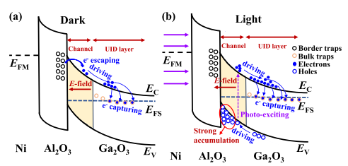
Fig. 5. Schematics illustrating the trapping and detrapping dynamics of border traps and UID bulk traps under (a) NBS and (b) NBIS with stress voltage of −5 V.
DOI:
doi.org/10.1109/TED.2026.3664283