Paper Sharing
【International Papers】Low temperature (600 °C) formation of Al₂O₃/β Ga₂O₃ interface with low interface state density employing substrate surface O₃ treatment processes
日期:2026-05-26阅读:127
Researchers from the University of Tokyo have published a dissertation titled "Low‑temperature (600 °C) formation of Al₂O₃/β‑Ga₂O₃ interface with low interface state density employing substrate‑surface O₃ treatment processes" in Applied Physics Letters.
Background
β‑Ga₂O₃ is expected to be a next‑generation power device material due to its large bandgap (4.4–4.7 eV) and high breakdown electric field. Additionally, the availability of bulk crystal growth from molten Ga₂O₃ using the EFG method is beneficial for the production of large‑diameter wafers, thereby enabling low‑cost wafer production. However, it remains challenging to realize high‑performance β‑Ga₂O₃‑based MOSFETs, and the key challenge is the formation of MOS gate stacks with low interface state density. Conventional processes require high‑temperature annealing over 1000 °C to reduce interface state density, but such high‑temperature oxidation will reduce carrier concentration and increase resistance of β‑Ga₂O₃ significantly, deteriorating its electrical properties. How to realize selective surface oxidation at low temperature while avoiding bulk oxidation is still an unsolved technical gap.
Abstract
The benefit of employing O₃ surface treatment of the β‑Ga₂O₃ substrate to fabricate metal–oxide–semiconductor (MOS) capacitors with atomic‑layer‑deposited (ALD) Al₂O₃ as dielectrics was investigated systematically to design a fabrication process at a sufficiently low temperature (600 °C) which is expected to avoid high‑temperature‑induced deterioration of the electrical characteristics of the β‑Ga₂O₃ substrate. With a post‑deposition annealing (PDA) at 600 °C, the MOS interface characteristics with low interface state density (Dᵢₜ) were achieved by performing O₃ surface treatment at 300 °C prior to deposition of Al₂O₃ and/or by using O₃ as the oxidant in ALD. The impact of the gas composition of the 600 °C PDA ambient for the stack fabricated with the above O₃ treatments was further investigated to reduce Dᵢₜ down to ~ 2 × 10¹⁰ eV⁻¹ cm⁻² at an energy level of 0.2 eV below the conduction band edge.
Highlights
Adopting 300 °C O₃ substrate surface pretreatment and O₃ oxidant during ALD to realize Al₂O₃/β‑Ga₂O₃ interface with low interface state density at 600 °C low temperature.
Optimizing gas composition of 600 °C post‑deposition annealing ambient, the interface state density can reach ~ 2 × 10¹⁰ eV⁻¹ cm⁻², comparable to 1000 °C high‑temperature annealing.
Low‑temperature process avoids bulk oxidation of β‑Ga₂O₃ and prevents deterioration of material electrical properties.
Low oxygen partial pressure post‑deposition annealing can reduce both interface state density and oxide trapped charge density simultaneously.
Conclusion
In conclusion, We investigated a low‑thermal‑budget process to suppress Al₂O₃/β‑Ga₂O₃ (001) MOS interface defects using a low‑temperature PDA at 600 °C. By conducting O₃ surface pretreatment and employing O₃ instead of H₂O as the oxidant for ALD growth of Al₂O₃, Dᵢₜ as low as ~ 2 × 10¹⁰ eV⁻¹ cm⁻² at the energy level of 0.2 eV below the conduction band edge of β‑Ga₂O₃ was achieved. Low pO₂ PDA was found to be beneficial in reducing both Dᵢₜ and Qₜᵣₐₚ than PDA in O₂ when O₃‑Al₂O₃ was employed. Consequently, the employment of O₃ surface treatments combined with low‑pO₂ PDA enables the formation of β‑Ga₂O₃ MOS interfaces with low defect densities even at a low PDA temperature of 600 °C.
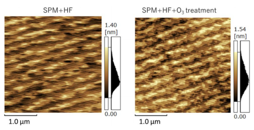
Figure 1. AFM images of the β‑Ga₂O₃ surfaces (a) with and (b) without O₃ surface treatment after SPM and HF cleaning.
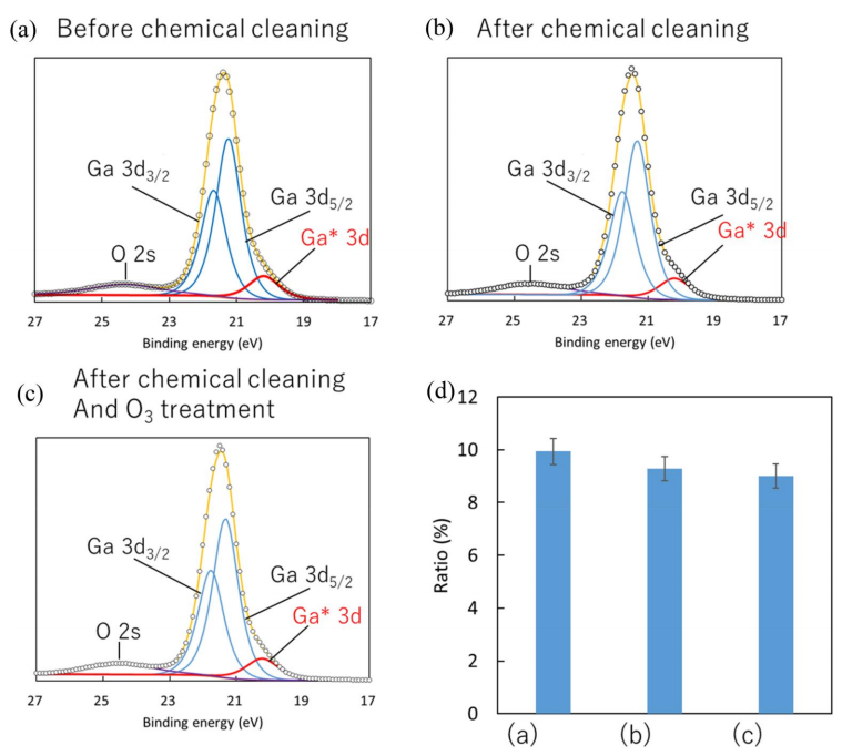
Figure 2. XPS Ga 3d spectra of the samples (a) before and (b) after chemical cleaning, and (c) after subsequent O₃ surface treatment. (d) Comparison of the area ratio of the Ga sub‑oxide component to the total Ga 3d spectrum for each sample.
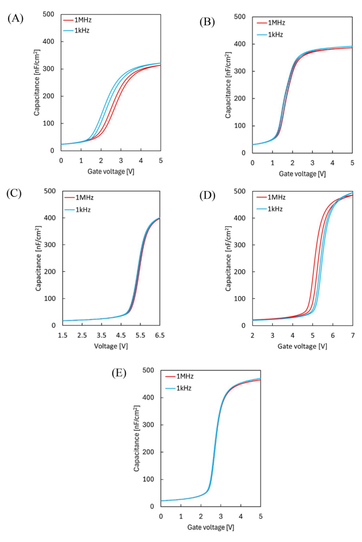
Figure 3. Bidirectional C–V characteristics of samples (a)–(e). (a) H₂O–Al₂O₃ without O₃ surface pretreatment; (b) H₂O–Al₂O₃ with O₃ surface pretreatment; and (c) O₃–Al₂O₃ with O₃ surface pretreatment. Samples (a)–(c) were subjected to PDA at 600 °C in an O₂ ambient. (d) O₃–Al₂O₃ with O₃ surface pretreatment, followed by PDA at 600 °C in an O₂ ambient, and (e) the same stack followed by PDA at 600 °C in a 0.1% O₂ + N₂ ambient.
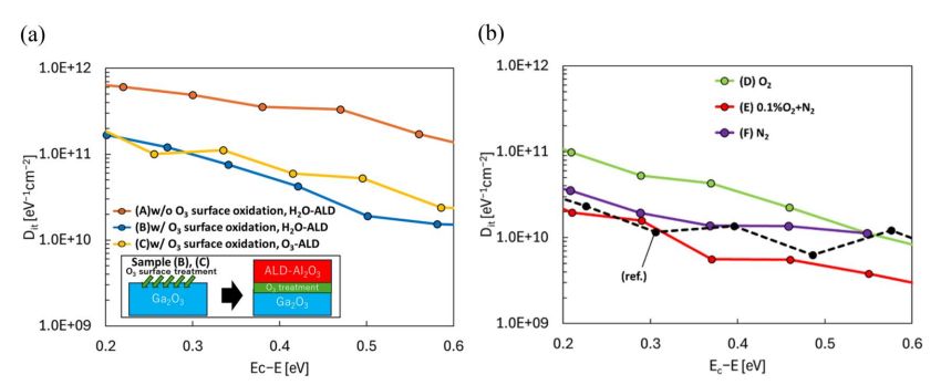
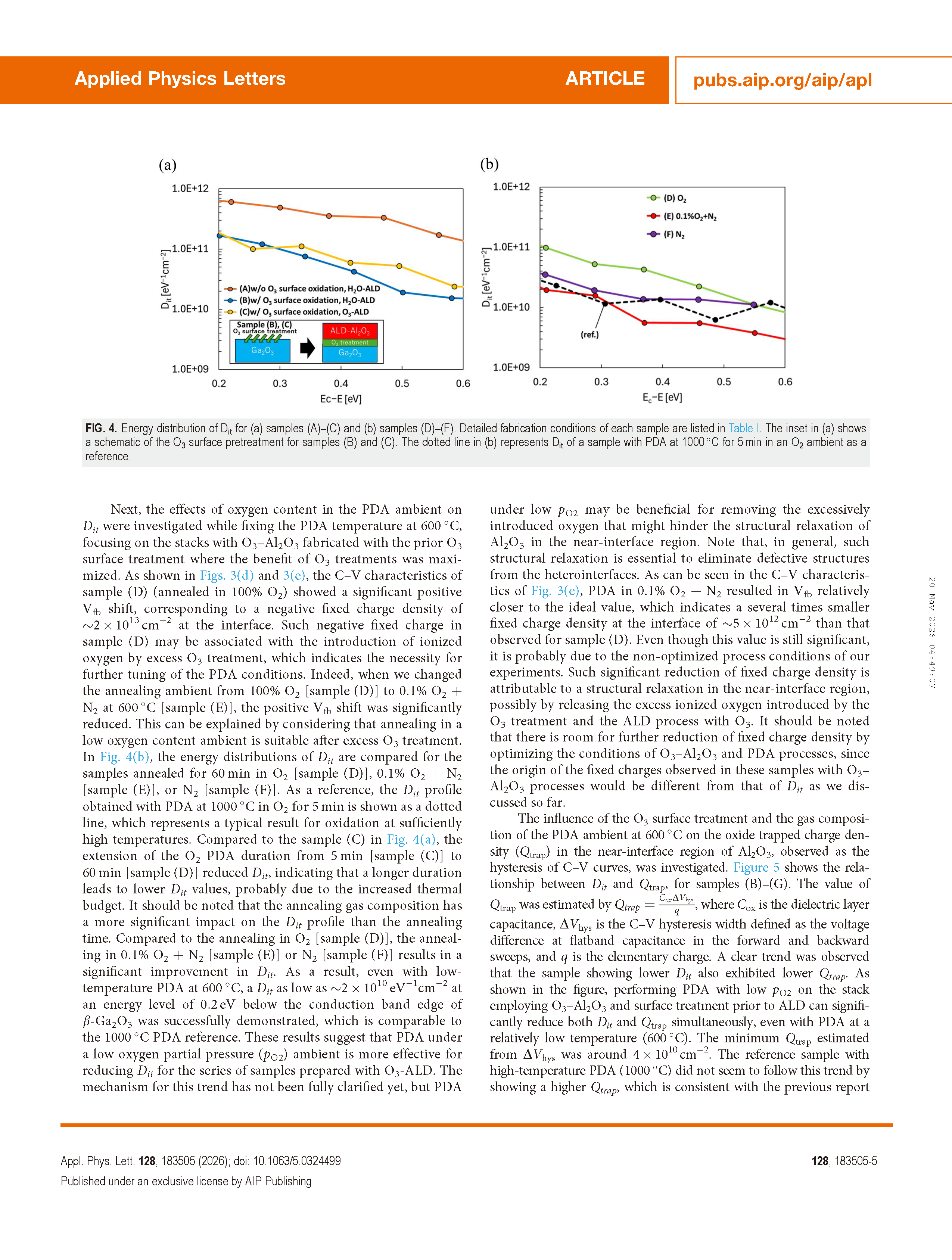
Figure 4. Energy distribution of Dᵢₜ for (a) samples (A)–(C) and (b) samples (D)–(F). Detailed fabrication conditions of each sample are listed in Table I. The inset in (a) shows a schematic of the O₃ surface pretreatment for samples (B) and (C). The dotted line in (b) represents Dᵢₜ of a sample with PDA at 1000 °C for 5 min in an O₂ ambient as a reference.
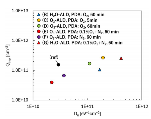
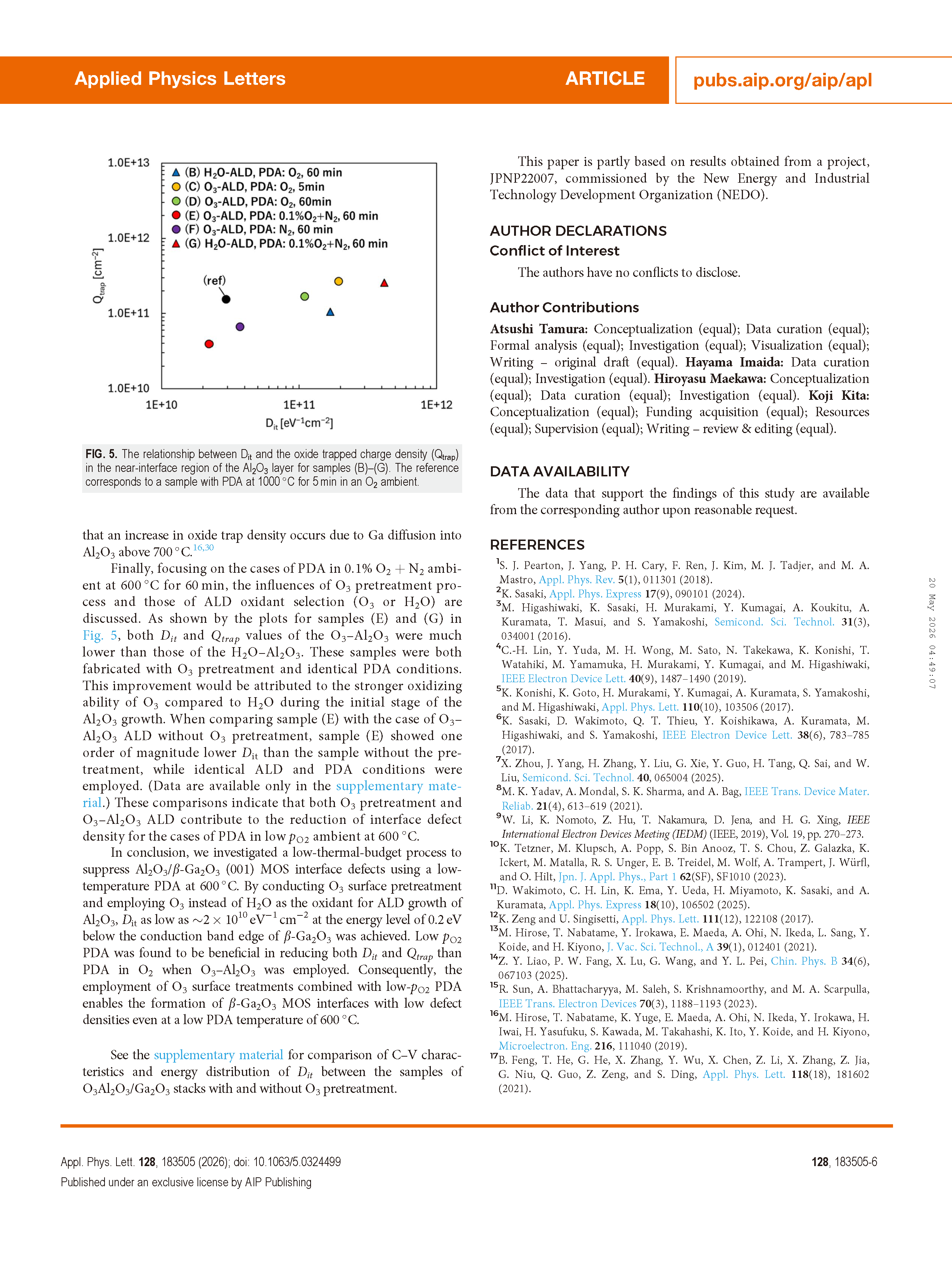
Figure 5. The relationship between Dᵢₜ and the oxide trapped charge density (Qₜᵣₐₚ) in the near‑interface region of the Al₂O₃ layer for samples (B)–(G). The reference corresponds to a sample with PDA at 1000 °C for 5 min in an O₂ ambient.
DOI:
doi.org/10.1063/5.0324499