


Member News
【Member News】Fujia Gallium Deeply Involved: Ga₂O₃ Photoconductive Switch Achievement with Near 100% Voltage Conversion Efficiency Graces Cover of Top Optics Journal
日期:2026-05-26阅读:244
Recently, Opto-Electronic Science, a flagship international optics journal, published an online cover article highlighting a heavyweight research breakthrough in gallium oxide (Ga₂O₃) photoconductive semiconductor switches (PCSS). The paper is titled "Phonon-assisted absorption photoconductive switch."
This research was spearheaded by Professor Wei Zheng’s team from the School of Materials, Sun Yat-sen University, and co-accomplished by Research Fellow Zhan Sui’s team from the Shanghai Institute of Laser Plasma, China Academy of Engineering Physics. Key contributions were made through the deep participation of Dr. Duanyang Chen from Hangzhou Fujia Gallium Technology Co., Ltd., and Research Fellow Hongji Qi from the Shanghai Institute of Optics and Fine Mechanics, Chinese Academy of Sciences / Shanghai Key Laboratory of Wide and Ultra-Wide Bandgap Semiconductor Materials.
Figure 1 Cover of the journal Opto-Electronic Science
With the rapid development of the low-altitude economy, civilian airports, critical infrastructure, and other scenarios face emerging security threats such as uncooperative drone intrusions. High-power microwave (HPM) technology, leveraging its directional electromagnetic radiation interference capabilities, has become one of the core technical pathways with immense application potential in the field of low-altitude security. As a key component in constructing miniaturized HPM emission systems, the photoconductive semiconductor switch (PCSS) possesses critical performance indicators—such as voltage-blocking capability, energy conversion efficiency, and output power density—that directly determine the system's degree of miniaturization and practical applicability.
Traditional PCSS devices heavily rely on materials like gallium arsenide (GaAs), which feature limited breakdown field strength and high-voltage operational capacity. Although emerging gallium oxide (Ga₂O₃)-based switches offer material advantages like an ultra-wide bandgap (approx. 4.9 eV) and high thermal stability, existing devices generally employ excitation methods based on impurity-level absorption, resulting in inherent bottlenecks of low voltage conversion efficiency and high conduction loss. To tackle this challenge, Professor Wei Zheng’s team originally proposed and validated a novel carrier excitation mechanism based on phonon-assisted absorption. By realizing highly efficient carrier bulk excitation within the Ga₂O₃ crystal through phonon coupling, they broke through the bottleneck of voltage conversion efficiency from the underlying physics, disrupting the industry's traditional understanding of excitation methods for ultra-wide bandgap semiconductor photoconductive devices.
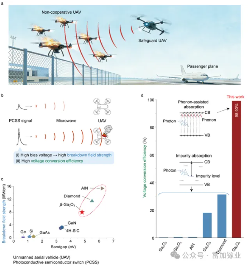
Fig. 2 High-power photoconductive semiconductor switches (PCSSs), acting as core components in high-power microwave systems, are applicable for low-altitude security assurance in critical infrastructures like civilian airports. In this work, Ga₂O₃ characterized by superior voltage-withstanding merits was employed to fabricate PCSSs, achieving a remarkable voltage conversion efficiency of 98.93% via the phonon-assisted absorption mechanism.
The experimental findings reveal the exceptional performance metrics of the device: under an ultra-high bias voltage of 4000 V and an excitation energy of 1.98 mJ, a peak output voltage of 3957 V is obtained, corresponding to a voltage conversion efficiency of up to 98.93% that approaches the fundamental physical limit. The peak output power density reaches 17.7 MW/cm². Over a broad bias voltage range spanning from 50 V to 4000 V, the full width at half maximum (FWHM) of the output voltage's relative deviation is only 3.01%, showcasing superior operational stability. The aforementioned parameters represent the state-of-the-art comprehensive performance among the reported Ga₂O₃ PCSSs to date.
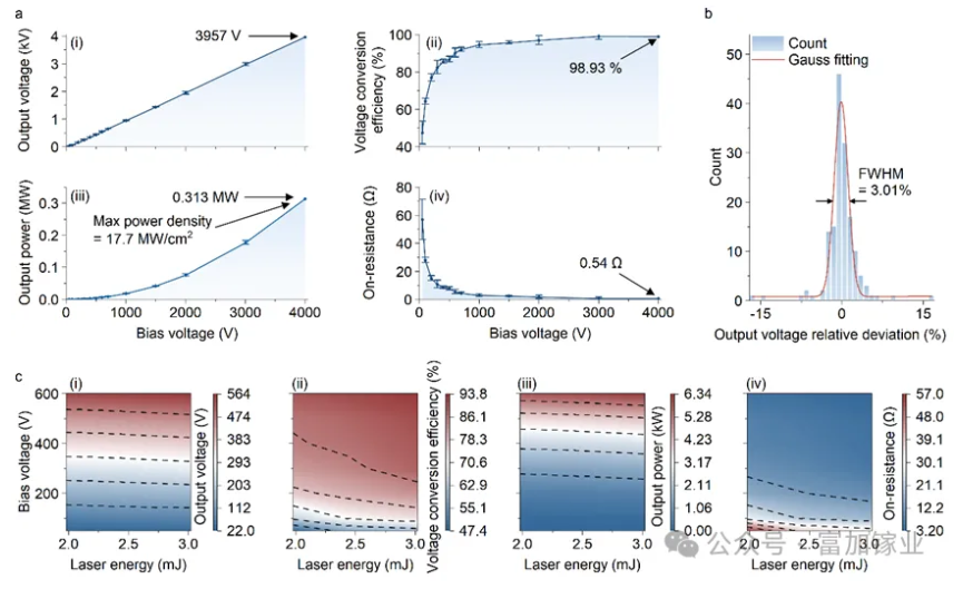
Fig. 3 Ga₂O₃ photoconductive semiconductor switches exhibit superior performance under a wide bias voltage range of 50–4000 V, featuring a voltage conversion efficiency of 98.93% and a peak output power density of 17.7 MW/cm².
The achievement introduces a novel physical paradigm and technical route for the architecture of high-power, high-efficiency microwave systems. It exhibits extensive engineering application prospects in areas including low-altitude security, national defense safety, and specialized electronics, establishing a pivotal device foundation for transitioning high-power microwave technology from laboratory innovation to practical hardware deployment.
Fujia Gallium spearheaded the key material support in this study by delivering ultra-high-quality iron-doped Ga₂O₃ single crystals to the research group. Capitalizing on this world-class frontier milestone, Fujia Gallium will consistently solidify its collaborative ties among industry, university, and research sectors with leading institutions. The company is committed to accelerating the commercialization of gallium oxide optoelectronic devices, adhering to its corporate mission of "Let the world use excellent materials," and devoting its core capabilities to achieving self-reliance and controllability for the country's fourth-generation semiconductor industry in high-end optoelectronic applications.
【Paper Information】
Wang Z, Zhang LX, Cheng L et al. Phonon-assisted absorption photoconductive switch. Opto-Electron Sci 5, 260011 (2026).
DOI: https://doi.org/10.29026/oes.2026.260011 Received: March 12, 2026; Accepted: April 29, 2026; Published Online: May 20, 2026
Product Portfolio
Gallium Oxide Crystal Growth Equipment
Fujia Gallium has developed the world’s first EFG crystal growth system featuring a proprietary “one-click crystal growth” function, supporting 2-inch to 6-inch crystal production. The system is protected by 6 granted domestic patents and 4 international patents. Complete equipment solutions and process packages are available.
The company has also independently developed fully automated VB (Vertical Bridgman) crystal growth equipment. It was the first in China to overcome the technical bottleneck of 6-inch single-crystal growth using the VB method, enabling large-diameter bulk crystal production. This platform is supported by 6 granted domestic patents and 4 international patents, with customizable equipment and process solutions available.
Gallium Oxide Single-Crystal Substrates
As one of China’s earliest pioneers in Gallium Oxide single-crystal research and an industry-leading supplier, Fujia Gallium provides high-quality single-crystal substrates to global customers.
The product portfolio includes 26 standard substrate specifications ranging from 2-inch to 6-inch diameters. Customized solutions are available in terms of wafer size, electrical properties, and crystal orientation, supporting both advanced epitaxy R&D and volume production requirements.
Gallium Oxide Epitaxial Wafers
Built upon mature MOCVD (Metal-Organic Chemical Vapor Deposition) and MBE (Molecular Beam Epitaxy) platforms, Fujia Gallium offers 15 standard epitaxial wafer products from 2-inch to 6-inch formats, as well as customized MBE-based epitaxial structures.
The company provides integrated “substrate + epitaxy” solutions. A precise process control system enables customization of key parameters including epitaxial layer thickness, doping concentration, and compositional uniformity, meeting diverse requirements across different power levels and device architectures.
About Hangzhou Fujia Gallium
Hangzhou Fujia Gallium Technology Co., Ltd., established on December 31, 2019, is committed to the vision of “enabling the world with better materials” and focuses on the industrialization of ultra-wide bandgap Gallium Oxide semiconductor materials. Its core products include Gallium Oxide single-crystal substrates, MOCVD/MBE epitaxial wafers, and crystal growth equipment based on the Vertical Bridgman (VB) and Edge-Defined Film-Fed Growth (EFG) methods. The company provides systematic solutions for material development, accelerating the integration of the entire ultra-wide bandgap Gallium Oxide industry chain and promoting the application of Gallium Oxide materials in power devices, microwave RF devices, and optoelectronic detection. A series of major achievements in Gallium Oxide development have been featured by leading media outlets including CCTV-1, CCTV-2, People’s Daily, Xinhua News Agency, China Securities Journal, and The Paper.
In terms of corporate recognition, the company was designated as a Zhejiang Province Science and Technology SME in 2022, recognized as a National High-Tech Enterprise in 2023, and awarded the titles of Hangzhou High-Tech Enterprise R&D Center and Zhejiang “Specialized and Sophisticated” SME in 2024. In 2025, it obtained ISO 9001 Quality Management System certification (Certificate No. 20225Q20294R0M) and was also named a 2024 Hangzhou “New Eagle” Enterprise. In the Gallium Oxide field, the company is leading the drafting of the first national standard in this area and has undertaken one project from the National Development and Reform Commission and one from the Ministry of Industry and Information Technology, while participating in three additional national and provincial-level projects supported by the National Natural Science Foundation of China and regional authorities in Zhejiang and Shanghai. To date, the company has been granted 14 international patents (6 in the United States, 7 in Japan, and 1 in Europe), 42 domestic patents, three registered “Fujia Gallium” trademarks, and five software copyrights, including its proprietary “One-Click Crystal Growth” control software.
