Paper Sharing
【International Papers】Efficient Space Charge Current Injection in Silicon Implanted Fe-doped β-Ga₂O₃ Crystals Resulting in Extremely Low Thermal Breakdown Field
日期:2026-05-27阅读:129
Researchers from the Institute of Microelectronics of Barcelona (IMB-CSIC), Spain and Materials Center Leoben Forschung GmbH (MCL), Austria have published a dissertation titled "Efficient Space Charge Current Injection in Silicon Implanted Fe-doped β-Ga₂O₃ Crystals Resulting in Extremely Low Thermal Breakdown Field" in 2026 27th International Conference on Thermal, Mechanical and Multi-Physics Simulation and Experiments in Microelectronics and Microsystems (EuroSimE).
Background
Gallium oxide (Ga₂O₃) has emerged as a promising material for next-generation power devices due to its ultra-wide bandgap and high critical breakdown electric field. However, its thermal conductivity is much lower than that of SiC and GaN, leading to severe self-heating effects that limit its high-power applications. Most existing research has focused on optimizing heat dissipation structures, while the utilization of controlled thermal effects remains largely unexplored.
Abstract
In this work, we report an unusual and pronounced localized Joule heating phenomenon associated with quadratic transport regime in Fe-doped insulating β-Ga₂O₃ substrates incorporating a shallow silicon-implanted conductive channel. Devices consisting of concentric Ti/Au contacts separated by 10–30 µm exhibit a reproducible quadratic current–voltage dependence (I ∝ V²), characteristic of Space-Charge-Limited Current (SCLC) conduction. Thermal conductivity measurements performed using time-domain thermoreflectance (TDTR) reveal a reduction in thermal conductivity in the Si-implanted channel (12.5 ± 0.4 W/mK) compared to the Fe-doped bulk material (20.2 ± 0.6 W/mK), indicating increased phonon scattering due to implantation-induced lattice disorder. Under electrical bias, the non-uniform electric field distribution associated with SCLC leads to localized regions of enhanced Joule heating, resulting in strong temperature gradients and premature thermal breakdown at relatively low applied voltages (10–20 V). A coupled electrical–thermal model is proposed to describe the interplay between space-charge accumulation, electric-field redistribution, and Joule heating within the device. The results highlight the importance of electro-thermal effects in Ga₂O₃ lateral structures and suggest that controlled SCLC-induced heating may be exploited for efficient localized electrical heating applications operating at very low electrical power.
Highlights
A strong coupling phenomenon of SCLC quadratic transport and localized Joule heating is first observed in Si-implanted Fe-doped β-Ga₂O₃.
It is confirmed that ion implantation significantly reduces the thermal conductivity of Ga₂O₃ channels, providing direct experimental evidence for enhanced phonon scattering induced by lattice disorder.
A coupled electrical-thermal model is established to reveal the physical mechanism of premature thermal breakdown at low voltages.
A new application direction is proposed that controlled SCLC-induced heating can be utilized for low-power localized heating.
Conclusion
This work investigated the electrical and thermal behavior of Fe-doped β-Ga₂O₃ substrates incorporating a shallow Si-implanted conductive channel and lateral concentric metal contacts. Electrical measurements revealed a clear quadratic current–voltage dependence consistent with space-charge-limited current (SCLC) transport, enabled by efficient carrier injection through Ti/Au Ohmic contacts formed on the implanted region. Thermal characterization using time-domain thermoreflectance showed a significant reduction of thermal conductivity in the implanted layer compared to the bulk Fe-doped material, attributed to implantation-induced lattice disorder and enhanced phonon scattering. The combination of SCLC conduction and non-uniform electric field distribution leads to strongly localized Joule heating within the channel region. This electro-thermal coupling generates large temperature gradients and results in premature thermal breakdown at relatively low applied voltages. A simplified analytical model describing the spatial distribution of electric field and volumetric Joule heating in the SCLC regime was developed and shows good agreement with the experimental observations. These results highlight the significant role of electro-thermal effects in β-Ga₂O₃ devices, particularly in lateral geometries with short electrode spacing.
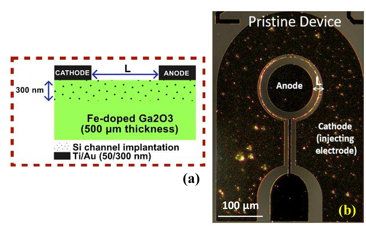
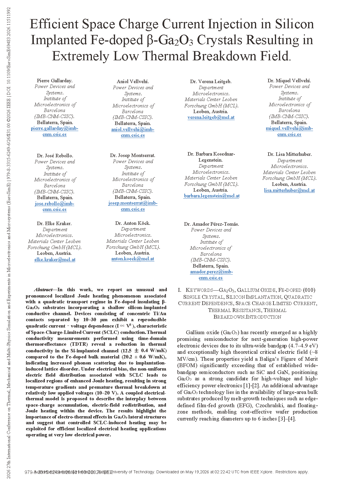
Figure 1 (a) Cross-sectional scheme of a fabricated device. (b) Optical image of a representative device.
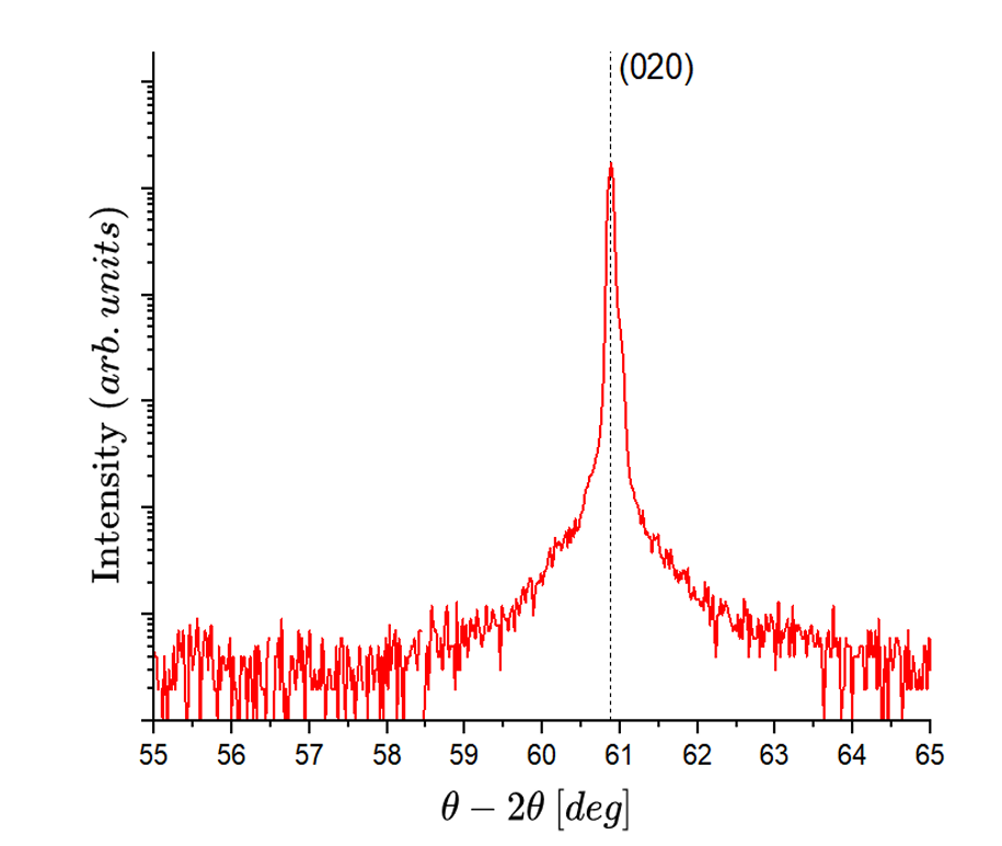
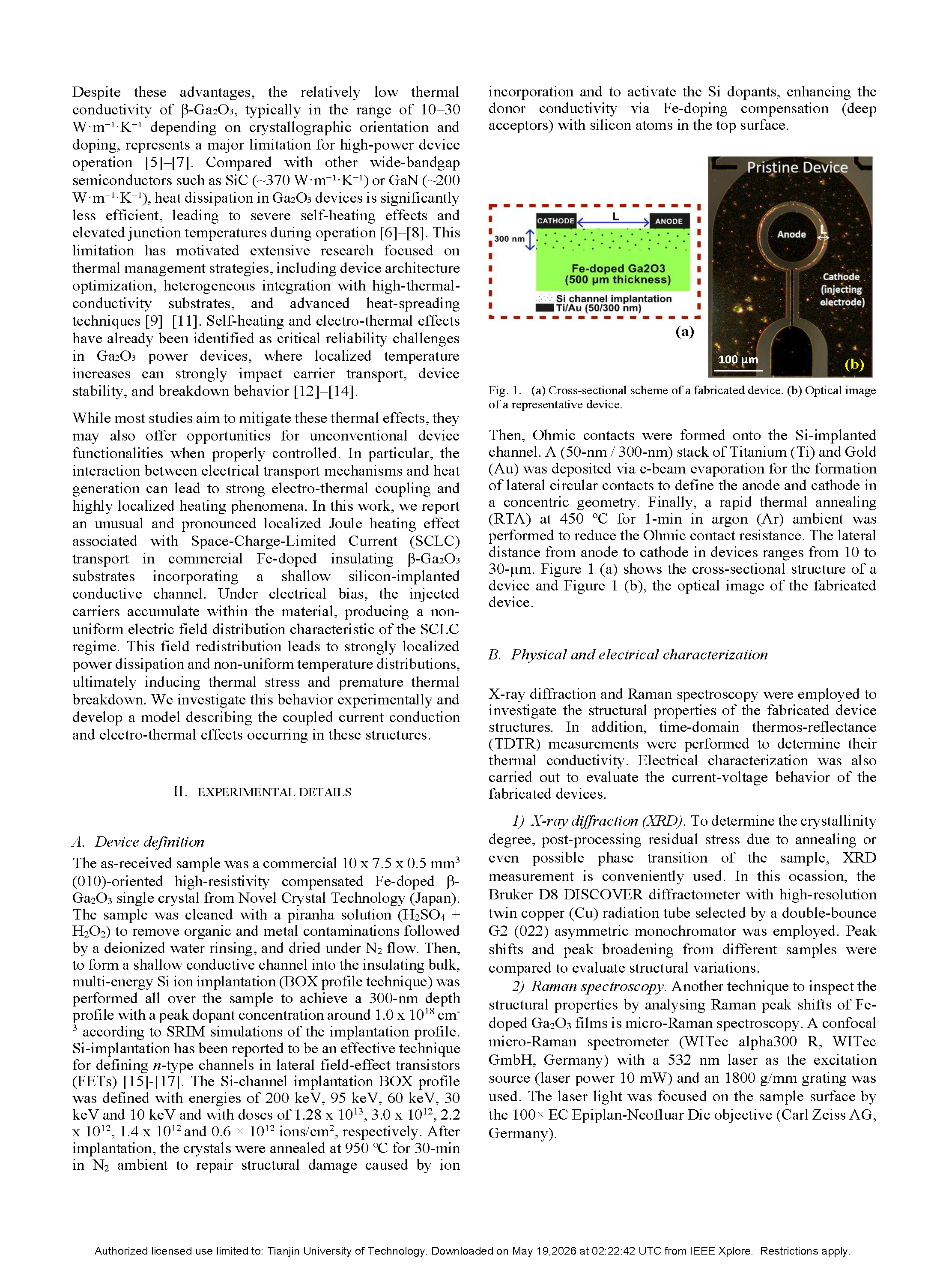
Figure 2 XRD peak of Fe-doped (010)-oriented β-Ga₂O₃ after silicon implantation and annealing at 950 ºC.
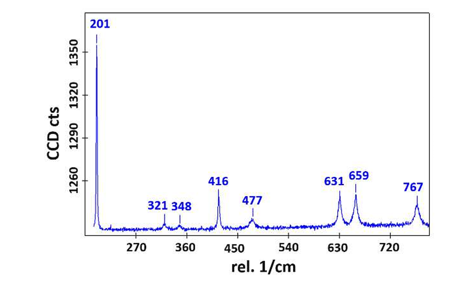
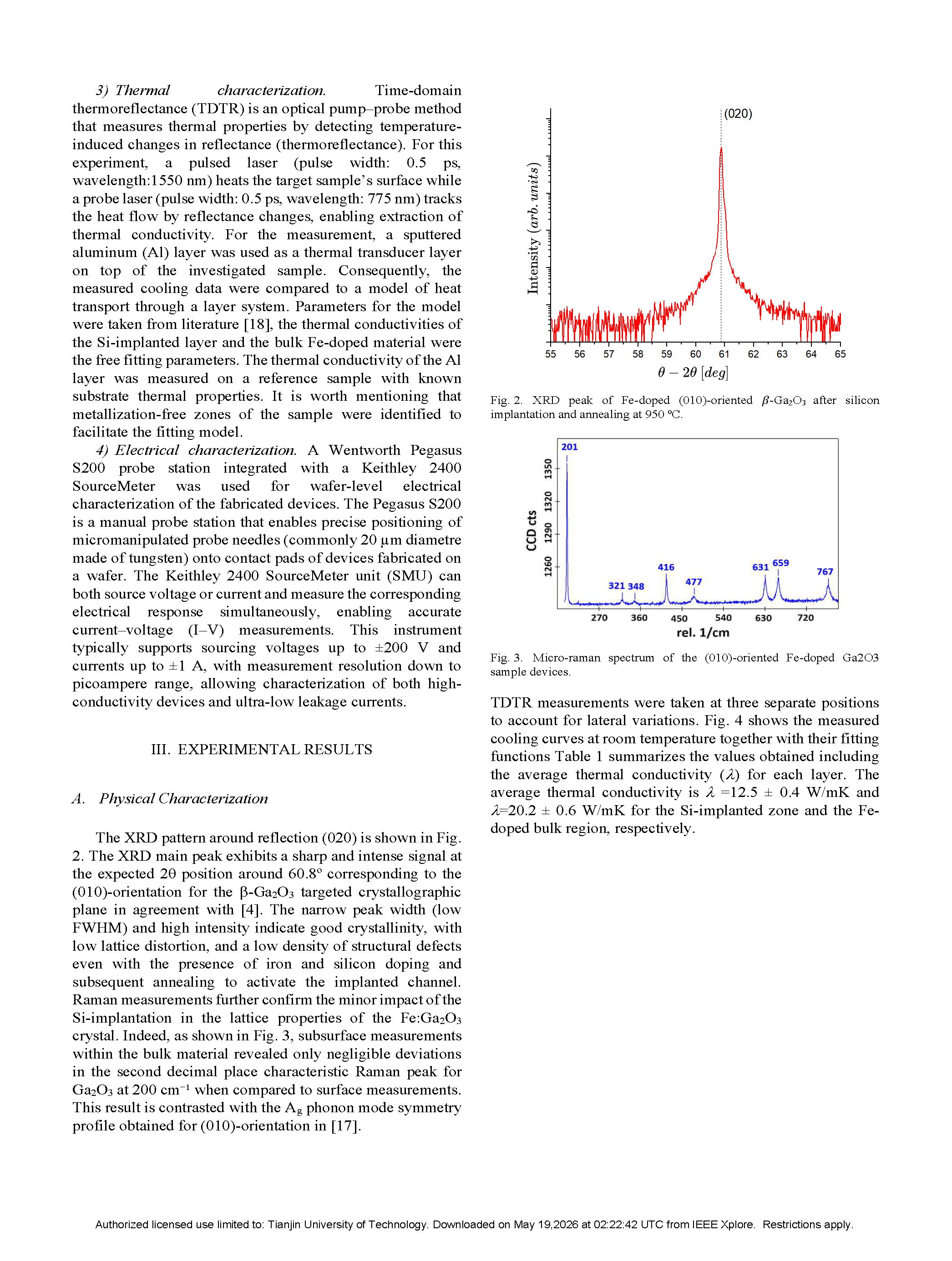
Figure 3 Micro-raman spectrum of the (010)-oriented Fe-doped Ga₂O₃ sample devices.
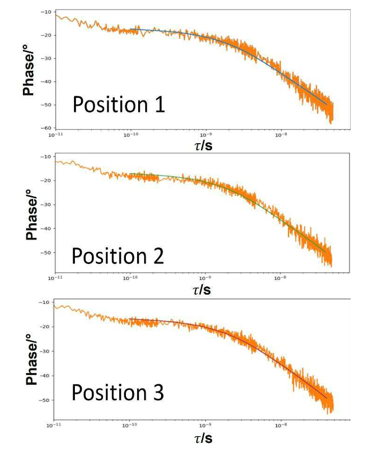
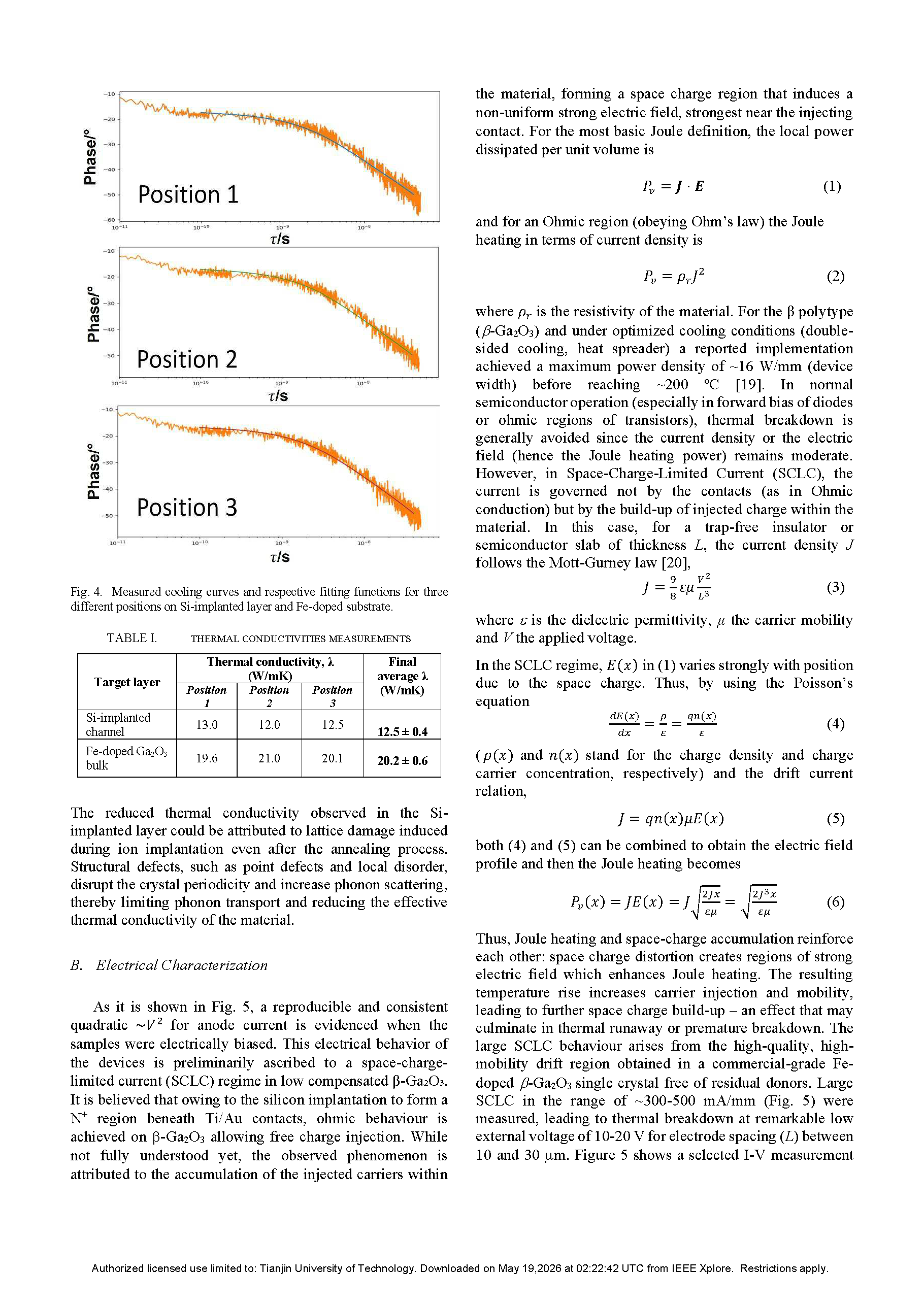
Figure 4 Measured cooling curves and respective fitting functions for three different positions on Si-implanted layer and Fe-doped substrate.
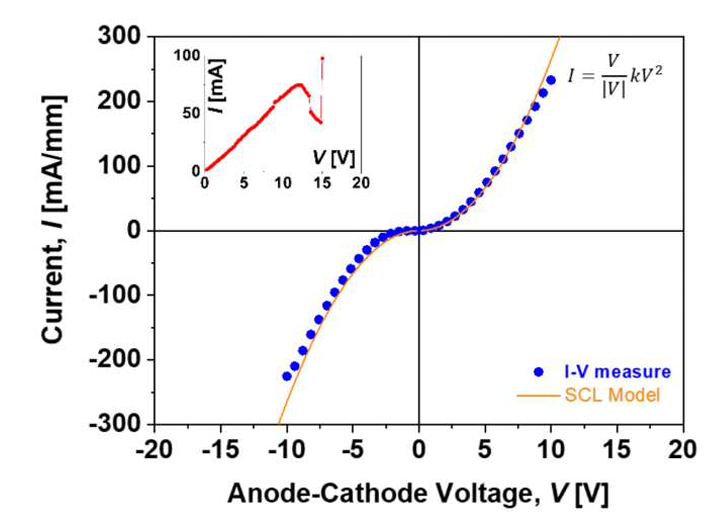
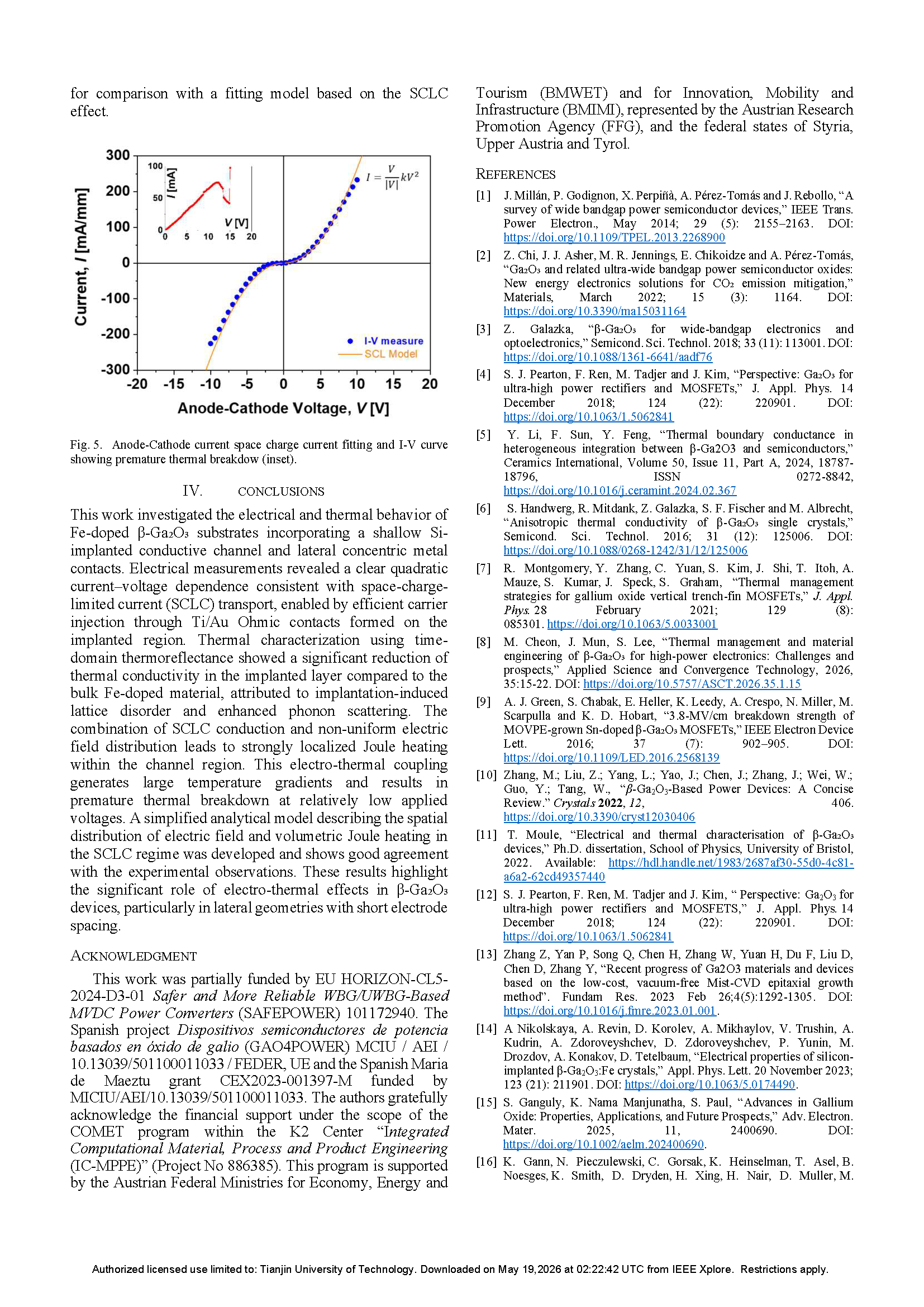
Figure 5 Anode-Cathode current space charge current fitting and I-V curve showing premature thermal breakdow (inset).
DOI:
10.1109/EuroSimE69483.2026.11511992