Paper Sharing
【Member Papers】Enhanced self-powered solar blind deep UV photodetector based on β-Ga₂O₃ homojunction with the synergistic regulation of Sn heavy doping and Schottky junctions
日期:2026-05-28阅读:151
Researchers from Northeast Normal University, Shandong University, Shanghai Dianji University, Institute of Materials Research and Engineering, Agency for Science Technology and Research, The City College of New York have published a dissertation titled "Enhanced self-powered solar blind deep UV photodetector based on β-Ga₂O₃ homojunction with the synergistic regulation of Sn heavy doping and Schottky junctions" in Applied Materials Today.
Background
Solar-blind deep UV detection is crucial for applications including missile early warning, secure communication, and ultraviolet astronomical detection. β-Ga₂O₃ has become a core material for next-generation high-performance detectors due to its intrinsic ultra-wide bandgap and natural solar-blind response. Traditional heteroepitaxy suffers from lattice mismatch and high defect density, while homoepitaxy can greatly improve crystal quality, but common orientations are prone to island growth and stacking faults, and research on the (011) orientation is scarce. Existing device optimization strategies can hardly simultaneously achieve dark current suppression, efficient photogenerated carrier separation, and fast response. There is a lack of efficient design based on the synergistic built-in electric fields of homojunctions and Schottky junctions, failing to meet the high-performance requirements of self-powered solar-blind detection.
Abstract
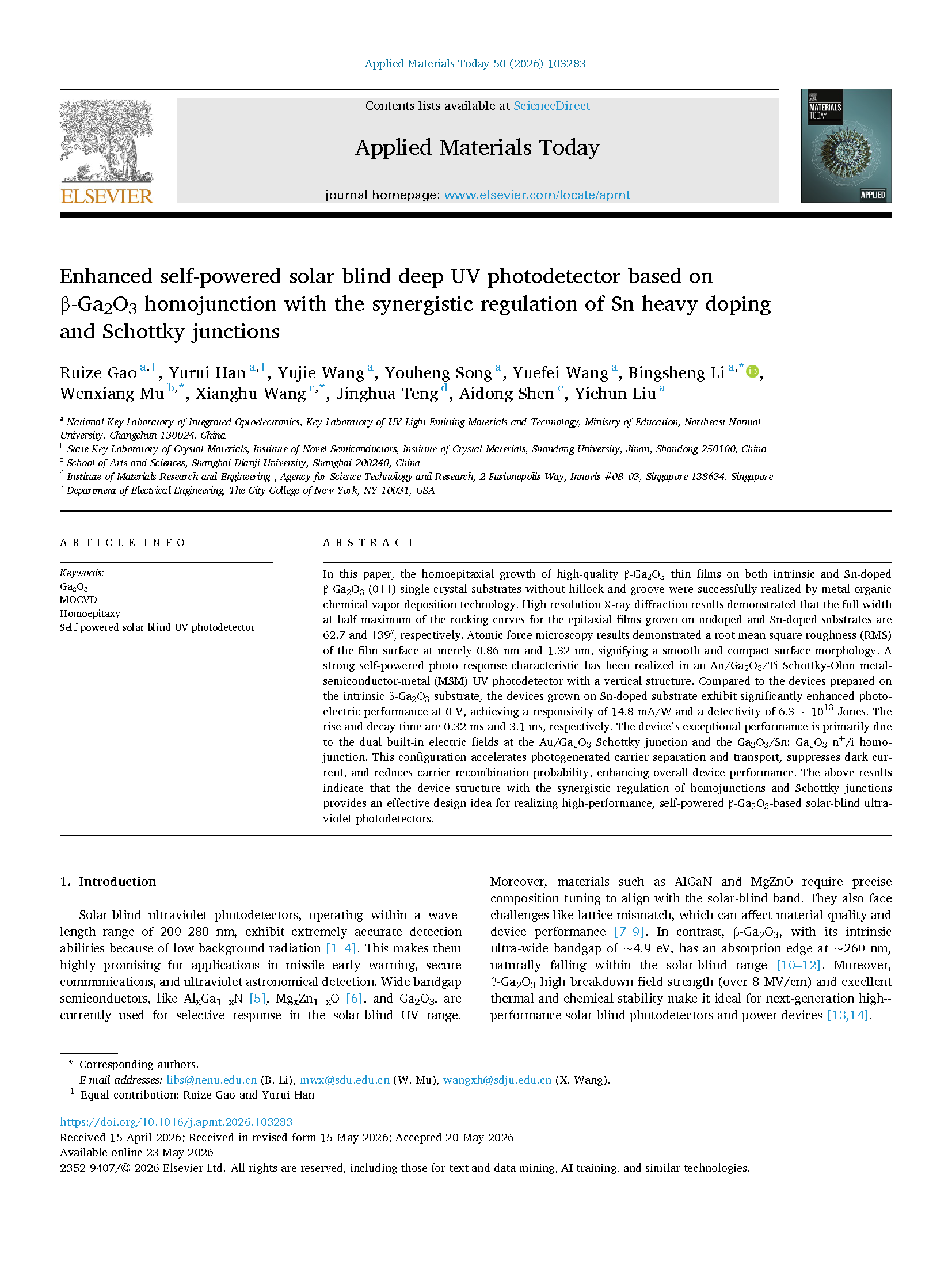
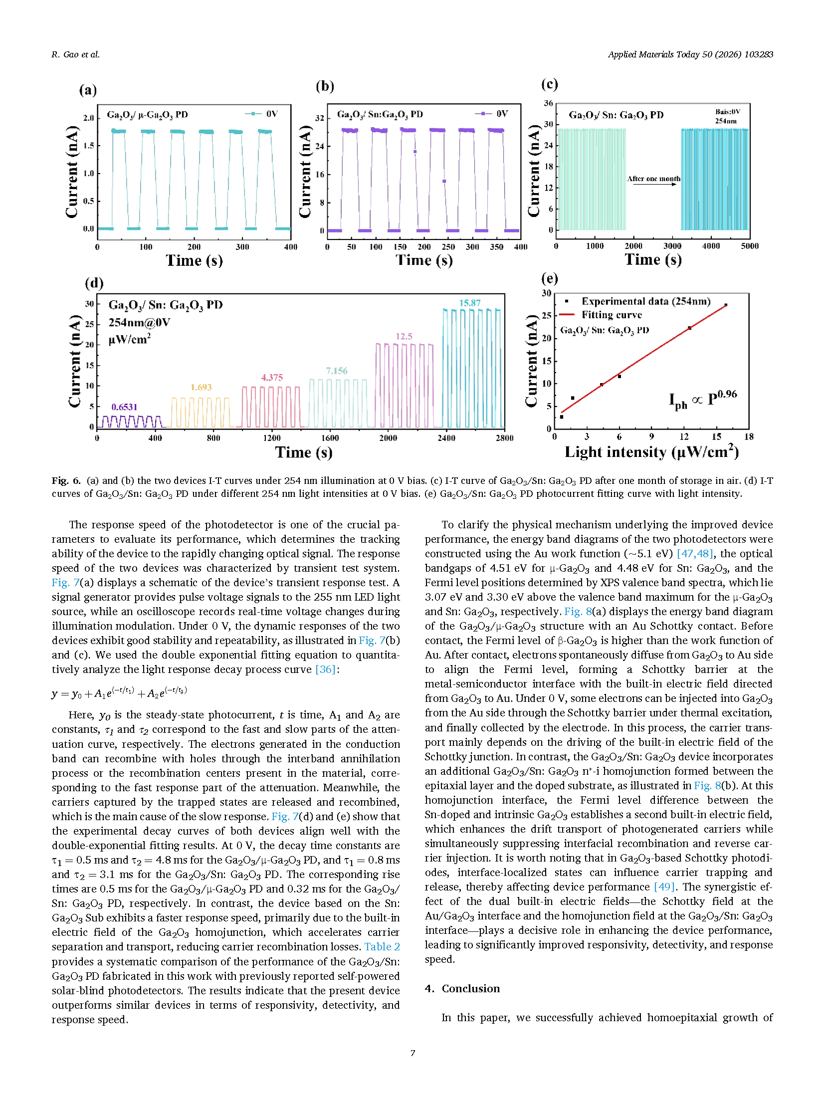
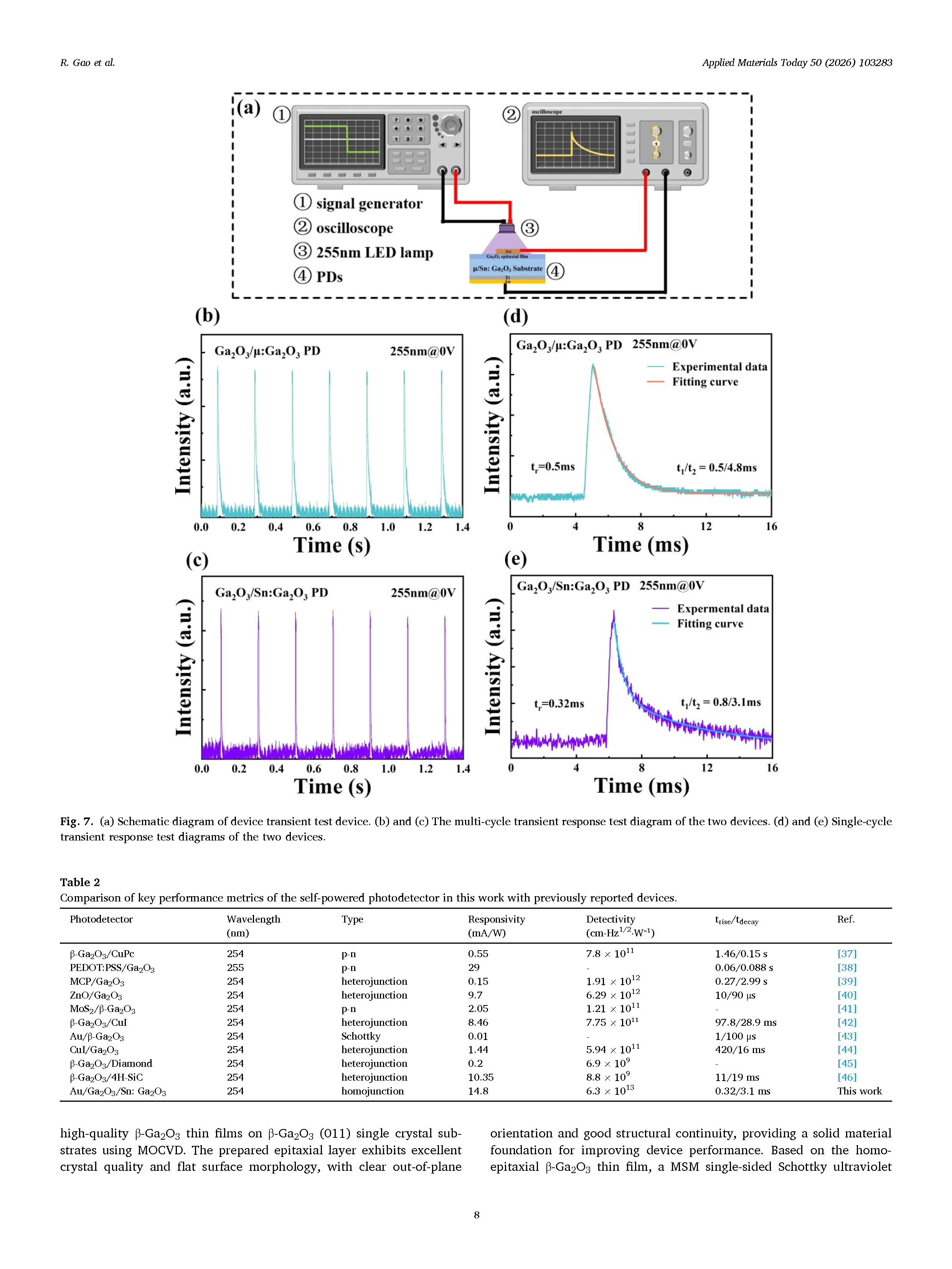
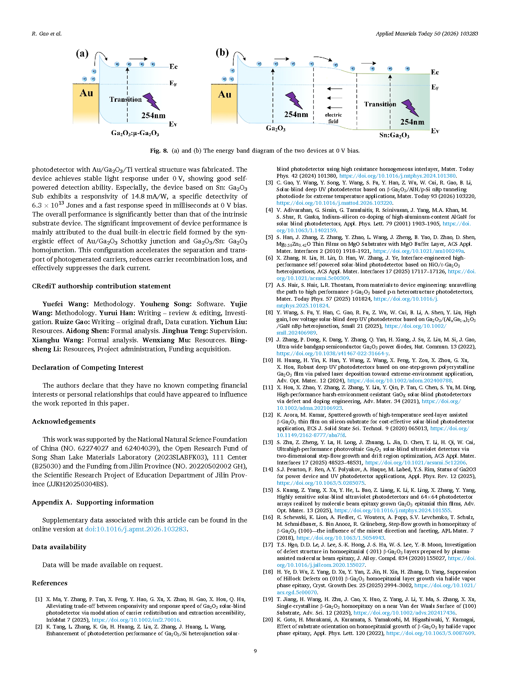
In this paper, the homoepitaxial growth of high-quality β-Ga₂O₃ thin films on both intrinsic and Sn-doped β-Ga₂O₃ (011) single crystal substrates without hillock and groove were successfully realized by metal organic chemical vapor deposition technology. High resolution X-ray diffraction results demonstrated that the full width at half maximum of the rocking curves for the epitaxial films grown on undoped and Sn-doped substrates are 62.7 and 139 arcsec, respectively. Atomic force microscopy results demonstrated a root mean square roughness (RMS) of the film surface at merely 0.86 nm and 1.32 nm, signifying a smooth and compact surface morphology. A strong self-powered photo response characteristic has been realized in an Au / Ga₂O₃ / Ti Schottky-Ohm metal-semiconductor-metal (MSM) UV photodetector with a vertical structure. Compared to the devices prepared on the intrinsic β-Ga₂O₃ substrate, the devices grown on Sn-doped substrate exhibit significantly enhanced photoelectric performance at 0 V, achieving a responsivity of 14.8 mA/W and a detectivity of 6.3 ×10¹³ Jones. The rise and decay time are 0.32 ms and 3.1 ms, respectively. The device’s exceptional performance is primarily due to the dual built-in electric fields at the Au / Ga₂O₃ Schottky junction and the Ga₂O₃ / Sn-Ga₂O₃ n/i homojunction. This configuration accelerates photogenerated carrier separation and transport, suppresses dark current, and reduces carrier recombination probability, enhancing overall device performance. The above results indicate that the device structure with the synergistic regulation of homojunctions and Schottky junctions provides an effective design idea for realizing high-performance, self-powered β-Ga₂O₃-based solar-blind ultraviolet photodetectors.
Highlights
First-time realization of defect-free high-quality homoepitaxy on β-Ga₂O₃ (011) substrates by MOCVD.
Construction of dual built-in electric fields synergistically regulated by Sn heavy doping and Schottky junctions for efficient self-powered solar-blind detection.
Self-powered device achieves 14.8 mA/W responsivity and an ultra-high detectivity of 6.3×10¹³ Jones.
Ultra-fast millisecond-order response speed with comprehensive performance superior to reported similar self-powered solar-blind detectors.
Conclusion
In this paper, we successfully achieved homoepitaxial growth of high-quality β-Ga₂O₃ thin films on β-Ga₂O₃ (011) single crystal substrates using MOCVD. The prepared epitaxial layer exhibits excellent crystal quality and flat surface morphology, with clear out-of-plane orientation and good structural continuity, providing a solid material foundation for improving device performance. Based on the homoepitaxial β-Ga₂O₃ thin film, a MSM single-sided Schottky ultraviolet photodetector with Au / Ga₂O₃ / Ti vertical structure was fabricated. The device achieves stable light response under 0 V, showing good self-powered detection ability. Especially, the device based on Sn: Ga₂O₃ Sub exhibits a responsivity of 14.8 mA/W, a specific detectivity of 6.3 ×10¹³ Jones and a fast response speed in milliseconds at 0 V bias. The overall performance is significantly better than that of the intrinsic substrate device. The significant improvement of device performance is mainly attributed to the dual built-in electric field formed by the synergistic effect of Au / Ga₂O₃ Schottky junction and Ga₂O₃ / Sn: Ga₂O₃ homojunction. This configuration accelerates the separation and transport of photogenerated carriers, reduces carrier recombination loss, and effectively suppresses the dark current.
Project Support
This work was supported by the National Natural Science Foundation of China (NO. 62274027 and 62404039), the Open Research Fund of Song Shan Lake Materials Laboratory (2023SLABFK03), 111 Center (B25030) and the Funding from Jilin Province (NO. 20220502002GH), the Scientific Research Project of Education Department of Jilin Province (JJKH20250304BS).
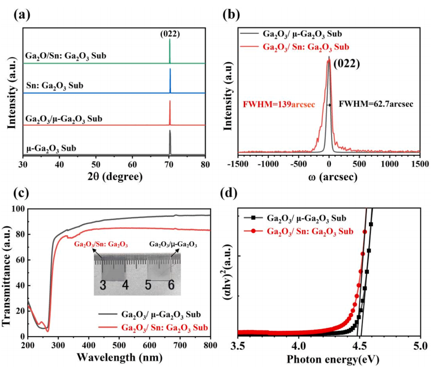
Fig. 1. (a) X-ray diffraction patterns of μ-Ga₂O₃ Sub and Sn: Ga₂O₃ Sub and epitaxial films. (b) XRD rocking curves of the two epitaxial films. (c) The transmission spectra of the two epitaxial films (the illustration is the physical map of the epitaxial film). (d) Band gap of two epitaxial films.
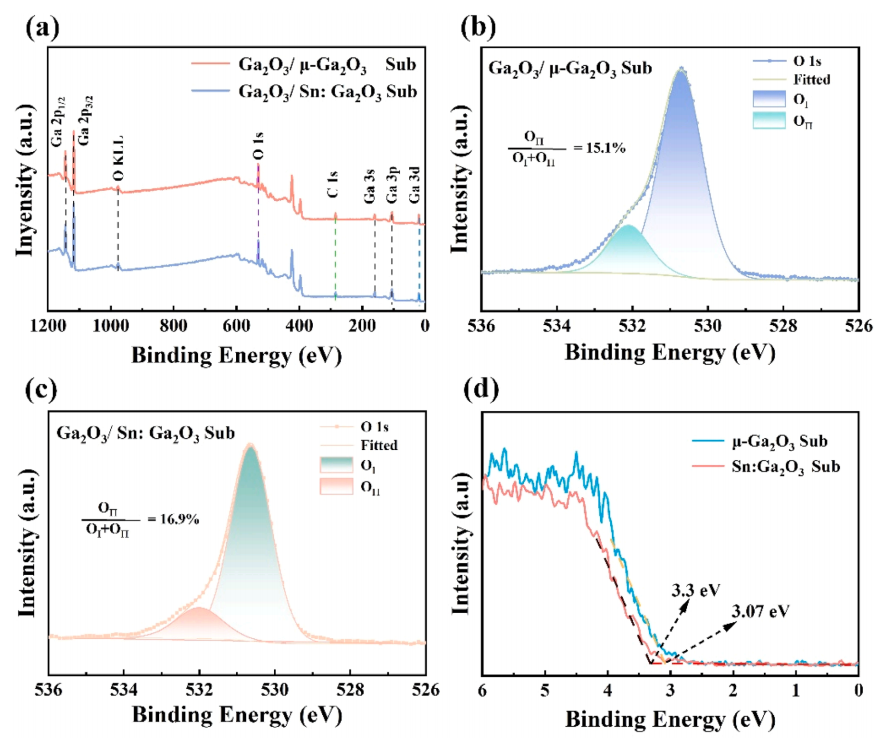
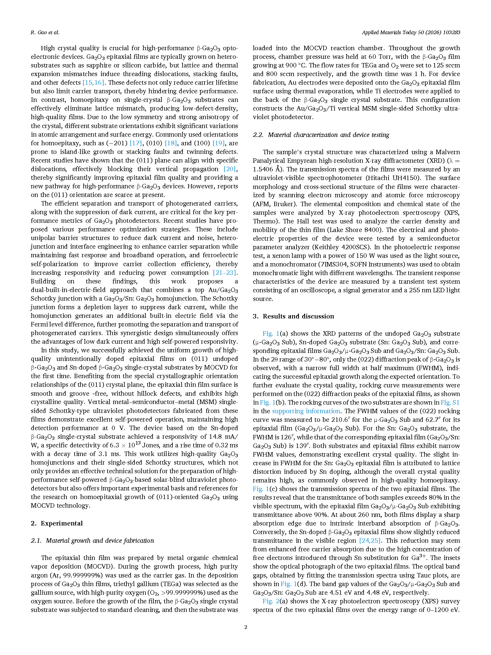
Fig. 2. (a) XPS survey spectra of the two epitaxial films. (b) and (c) O 1s spectra of the two epitaxial films. (d) VBM spectra of μ-Ga₂O₃ Sub and Sn: Ga₂O₃ Sub.
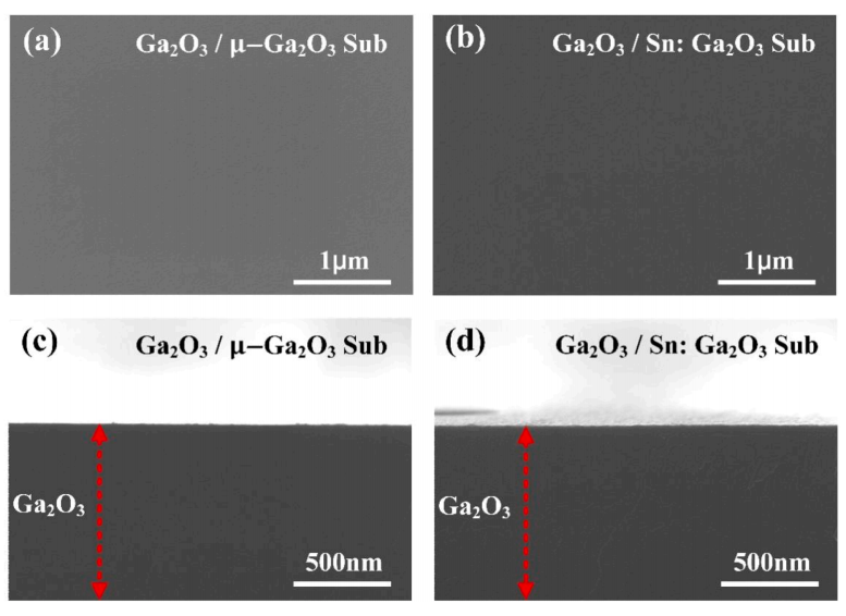
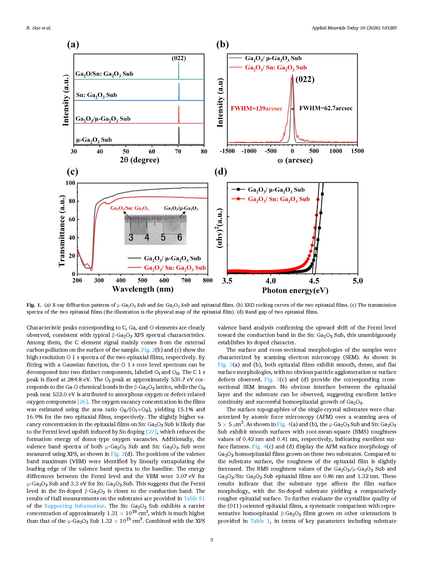
Fig. 3. (a) and (b) SEM surface images of the two epitaxial films. (c) and (d) Cross-sectional SEM view of two epitaxial films.
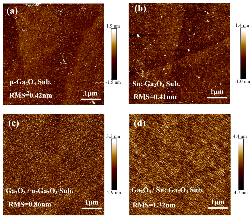
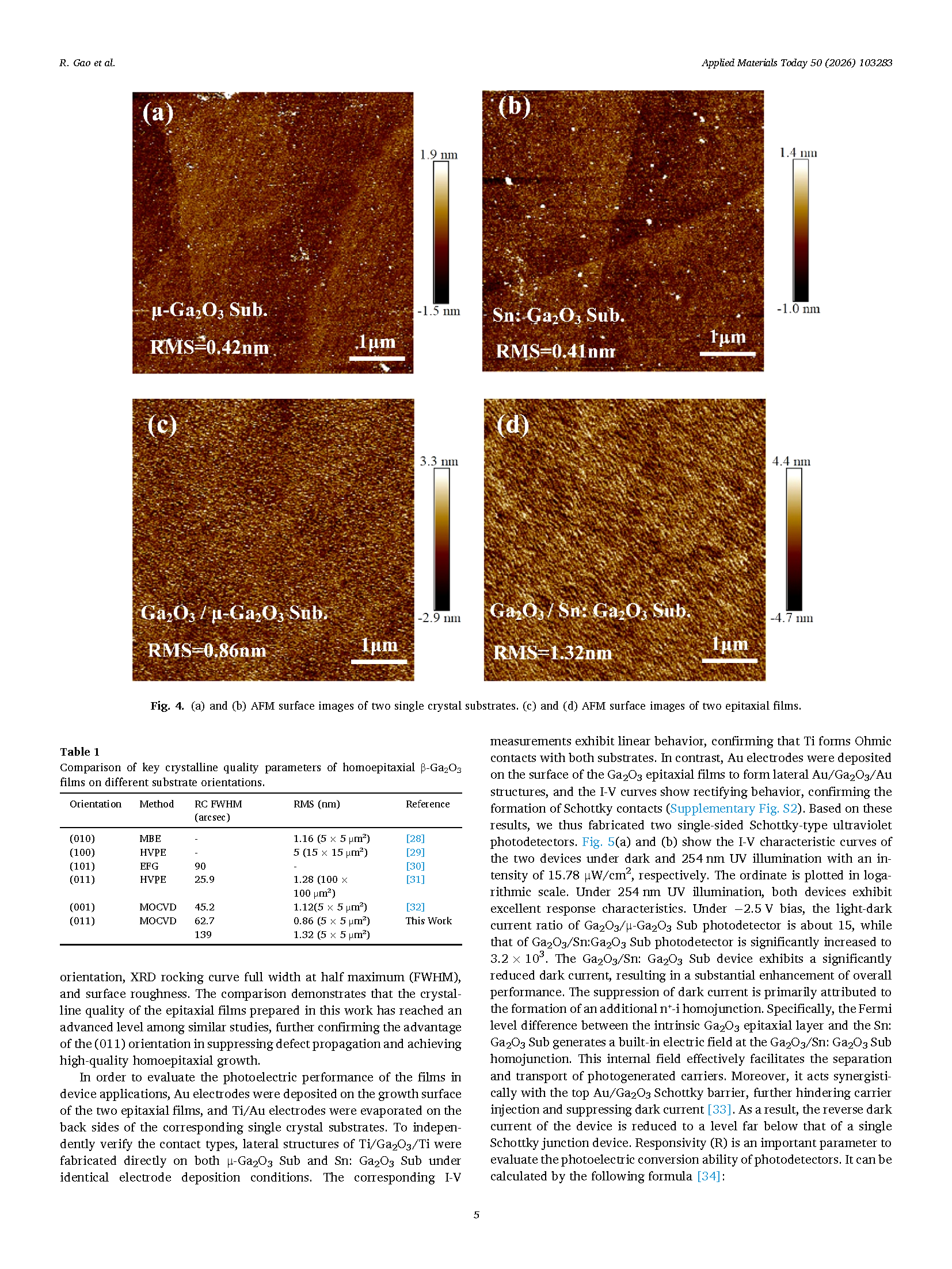
Fig. 4. (a) and (b) AFM surface images of two single crystal substrates. (c) and (d) AFM surface images of two epitaxial films.
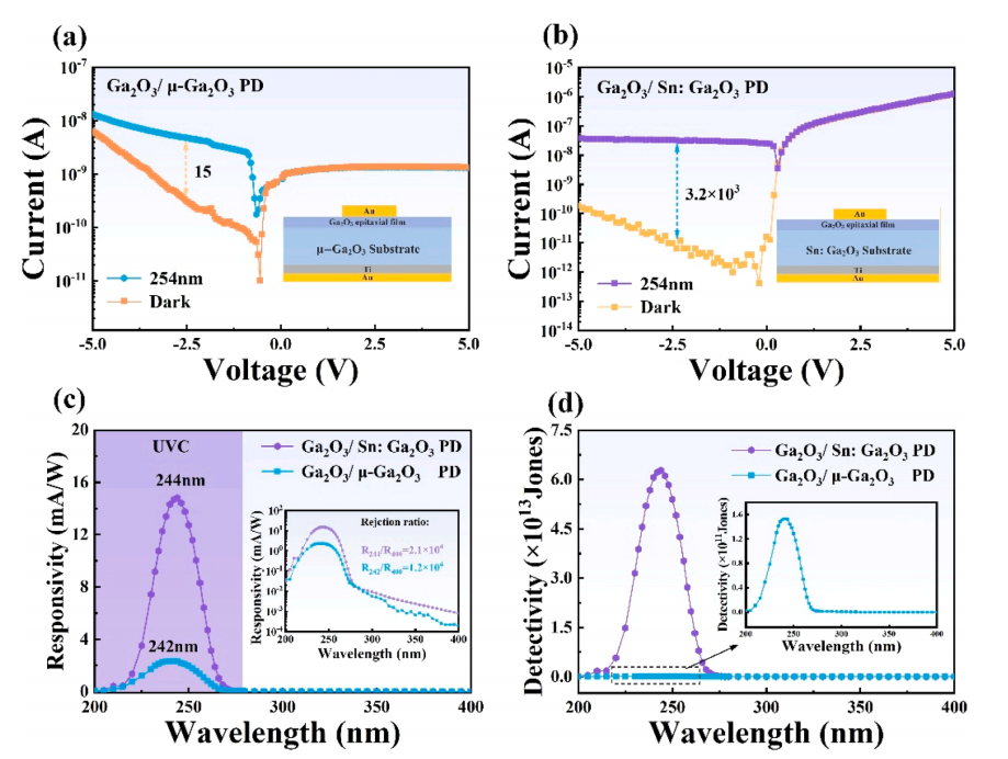
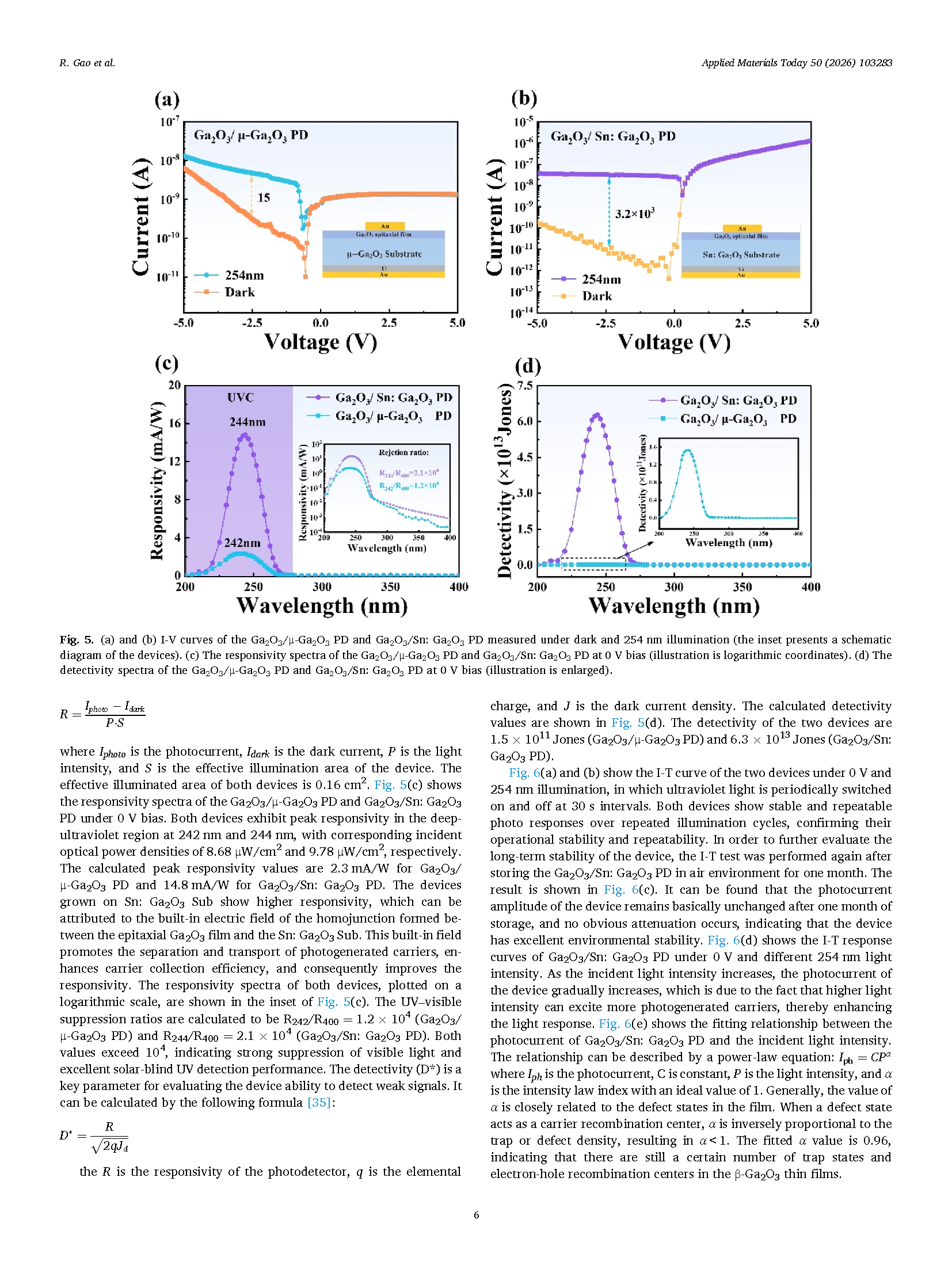
Fig. 5. (a) and (b) I-V curves of the Ga₂O₃ / μ-Ga₂O₃ PD and Ga₂O₃ / Sn: Ga₂O₃ PD measured under dark and 254 nm illumination (the inset presents a schematic diagram of the devices). (c) The responsivity spectra of the Ga₂O₃ / μ-Ga₂O₃ PD and Ga₂O₃ / Sn: Ga₂O₃ PD at 0 V bias (illustration is logarithmic coordinates). (d) The detectivity spectra of the Ga₂O₃ / μ-Ga₂O₃ PD and Ga₂O₃ / Sn: Ga₂O₃ PD at 0 V bias (illustration is enlarged).
DOI:
doi.org/10.1016/j.apmt.2026.103283