Paper Sharing
【Domestic Papers】Charged defect engineering modulates electroluminescent properties in Tb-doped Ga₂O₃/Al₂O₃ nanolaminates
日期:2026-05-29阅读:133
Researchers from the Nankai University have published a dissertation titled "Charged defect engineering modulates electroluminescent properties in Tb-doped Ga₂O₃/Al₂O₃ nanolaminates" in Journal of Alloys and Compounds.
Background
Silicon-based photonic integration is a promising solution to current bottlenecks in optoelectronics, such as signal crosstalk, power consumption and integration density. High-efficiency silicon-based electroluminescent materials are indispensable for silicon photonic integration. Terbium (Tb) doped oxide materials are promising for achieving green luminescence at ~540 nm with high color purity and narrow emission spectra, avoiding the “green gap” in III-V GaN-based LEDs. However, Tb-doped oxides suffer from poor conductivity, low excitation efficiency, high driving voltage and low luminous intensity. Al₂O₃ exhibits excellent transmittance and stability but poor electrical injection tolerance and easy breakdown. Ga₂O₃ is a wide-bandgap oxide semiconductor that can improve current injection tolerance and stability, while its mechanism for visible-light excitation remains unclear. Combining Ga₂O₃ and Al₂O₃ into nanolaminates is expected to achieve efficient visible-light excitation and reveal carrier injection differences between oxides.
Abstract
Green electroluminescence (EL) from silicon-based devices is achieved by precisely regulating the structure of Ga₂O₃/Al₂O₃:Tb nanolaminates using atomic layer deposition. The inherent negative charges, which originate primarily from oxygen vacancies and are more abundant in Ga₂O₃ than in Al₂O₃, are proved to be partially compensated by the Ga₂O₃-Al₂O₃ interfaces. This phenomenon enables a favorable balance between effective carrier injection and high excitation efficiency. The optimal Ga₂O₃/Al₂O₃:Tb EL device, annealed at 650°C with Ga₂O₃ and Al₂O₃ sublayers of comparable thickness, exhibits the emission intensity of 1.22 mW/cm² and the external quantum efficiency of 5.14%. The tolerance to injection current and the operation time of the Ga₂O₃/Al₂O₃:Tb devices could be improved by three orders of magnitude when the nanolaminates are predominantly composed of Ga₂O₃ content, at the expense of reduced EL intensity and lower excitation efficiency. This work explores the modulation mechanism and intrinsic factors enabling the strong and stable EL from rare earth-doped oxide nanolaminates.
Highlights
First precise modulation of electroluminescent properties in Ga₂O₃/Al₂O₃:Tb nanolaminates via charged defect engineering
Reveal charge compensation mechanism between oxygen vacancies and heterointerfaces
Achieve silicon-based Tb-doped green EL with EQE of 5.14%, superior to reported similar materials
Demonstrate that Ga₂O₃ content switches conduction mechanisms and greatly improves device stability
Conclusion
In summary, the investigation of ALD-fabricated Ga₂O₃/Al₂O₃:Tb nanolaminate MOSLEDs reveals the differences in optoelectronic performance are correlated with the balance of charged defects in the oxide nanolaminates. The negative charges, primarily arising from oxygen vacancies that are more abundant in Ga₂O₃ than in Al₂O₃, could be partially compensated by the Ga₂O₃-Al₂O₃ interfaces. Optimal green EL at 543 nm is obtained when using the annealing at 650 °C with the Ga₂O₃ and Al₂O₃ sublayers of comparable thickness, yielding the emission intensity of 1.22 mW/cm² and the EQE of 5.14%. The current-injection tolerance and the operation time of Ga₂O₃/Al₂O₃:Tb devices could be improved by three orders of magnitude when the nanolaminates are predominantly composed of Ga₂O₃ content, but the EL intensity and the radiative efficiency of doped Tb³⁺ ions are significantly reduced. The conduction mechanism is also determined by the different oxide matrices. The above results provide experimental results and mechanistic insights for the EL devices based on RE-doped oxide nanolaminates, contributing to the facilitation of the oxides and ALD technique in light-source applications.
Project Support
This work was supported by National Natural Science Foundation of China (No. 62275132).
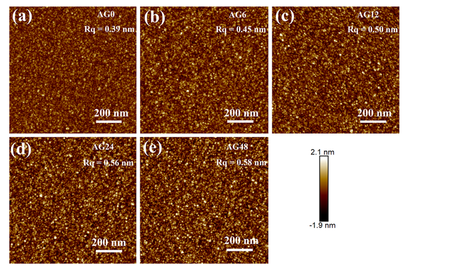
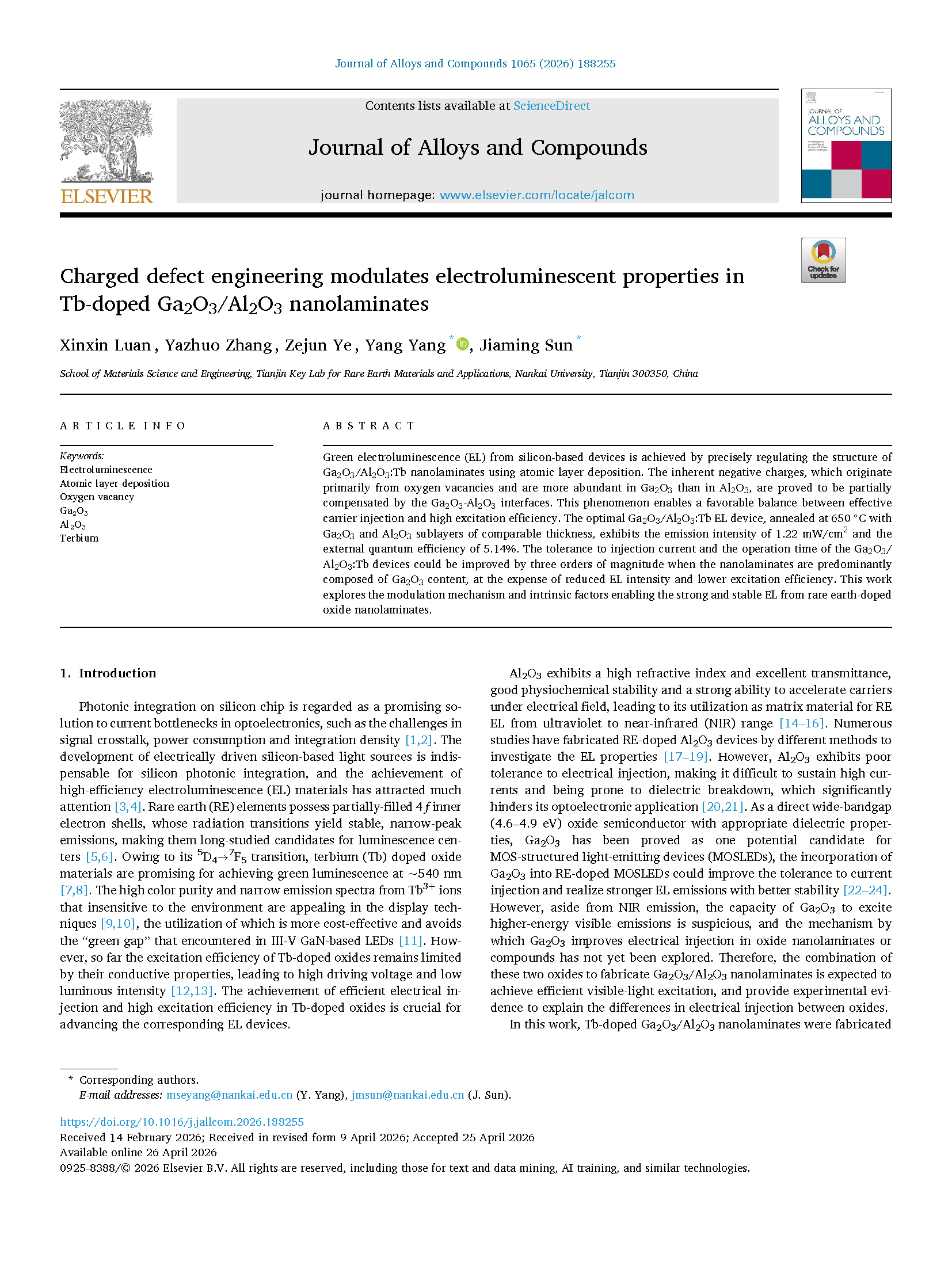
Figure 1 AFM images of the AGx nanofilms annealed at 650 ºC, the surface roughness values are correspondingly marked.
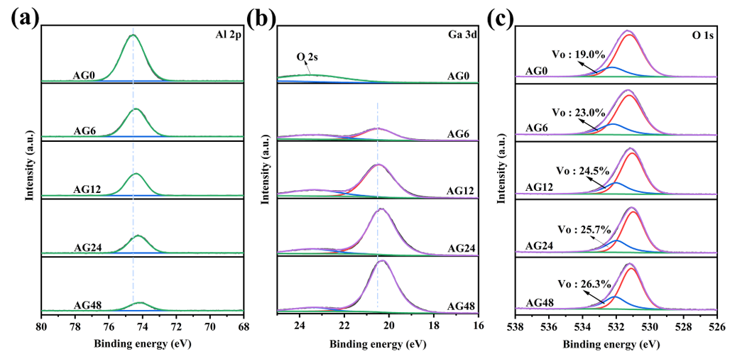
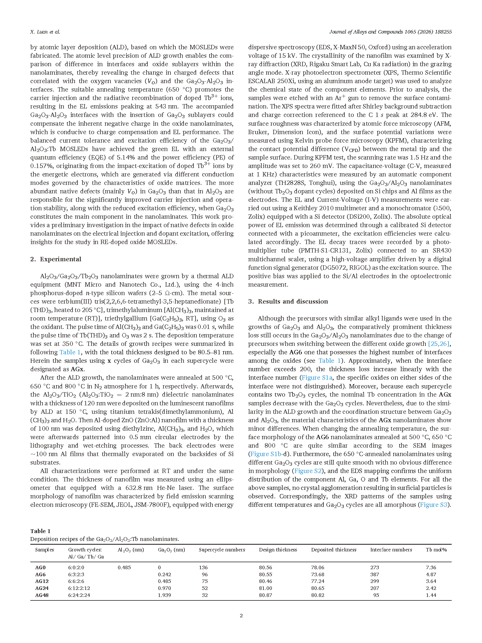
Figure 2 XPS spectra of the AGx nanofilms annealed at 650 ºC, showing the binding energies of (a) Al 2p, (b) Ga 3d and (c) O 1s signals.
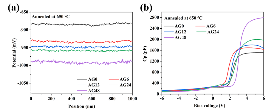
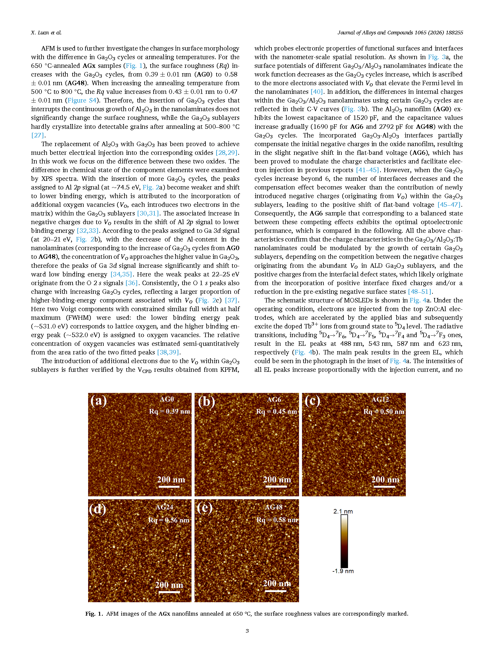
Figure 3 For the AGx nanofilms annealed at 650 °C, (a) the line-scan results of VCPD (contact potential difference) obtained from KPFM and (b) the C-V curves.
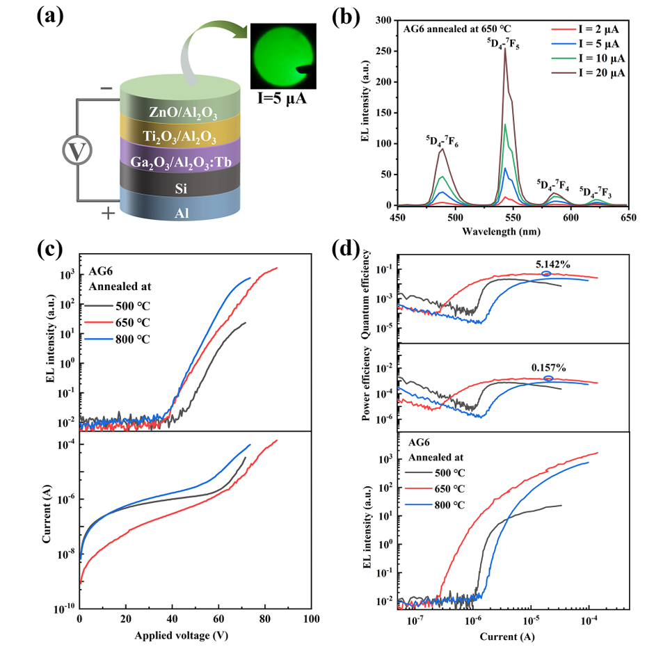
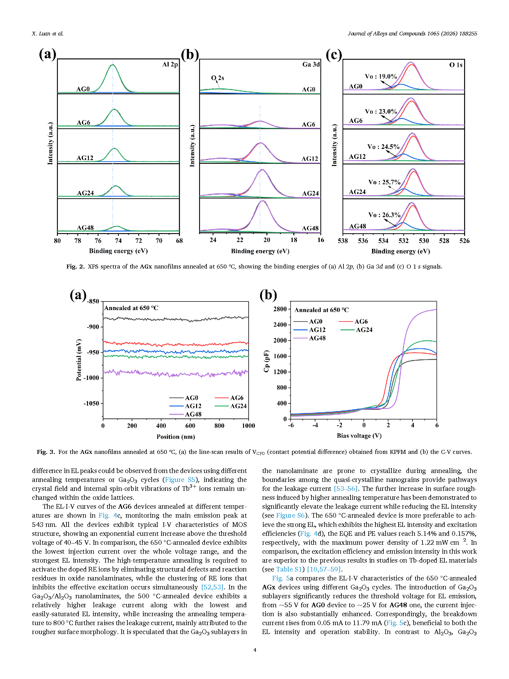
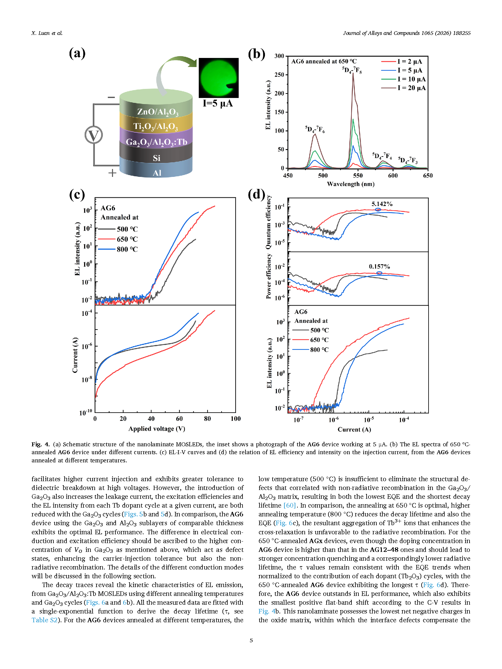
Figure 4 (a) Schematic structure of the nanolaminate MOSLEDs, the inset shows a photograph of the AG6 device working at 5 μA. (b) The EL spectra of 650 ºC-annealed AG6 device under different currents. (c) EL-I-V curves and (d) the relation of EL efficiency and intensity on the injection current, from the AG6 devices annealed at different temperatures.
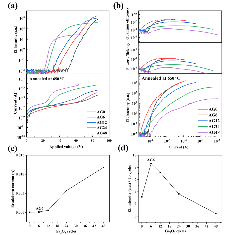
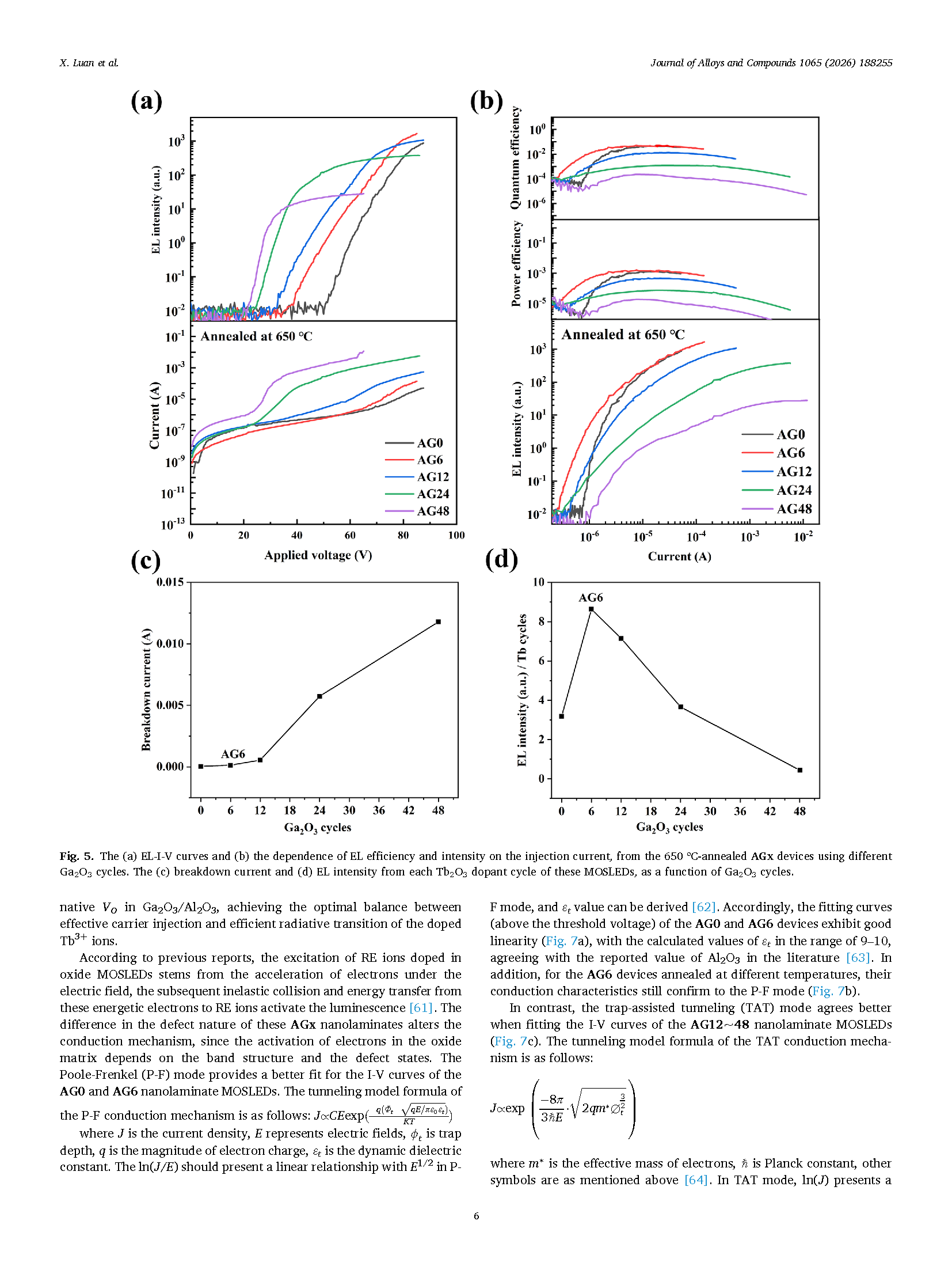
Figure 5 The (a) EL-I-V curves and (b) the dependence of EL efficiency and intensity on the injection current, from the 650 ºC-annealed AGx devices using different Ga₂O₃ cycles. The (c) breakdown current and (d) EL intensity from each Tb₂O₃ dopant cycle of these MOSLEDs, as a function of Ga₂O₃ cycles.
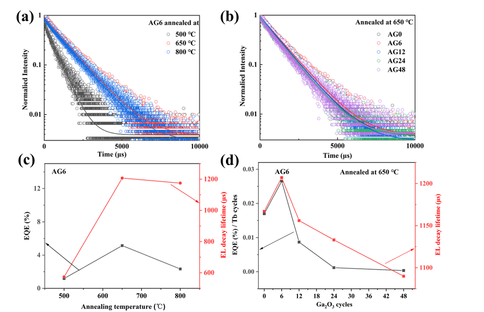
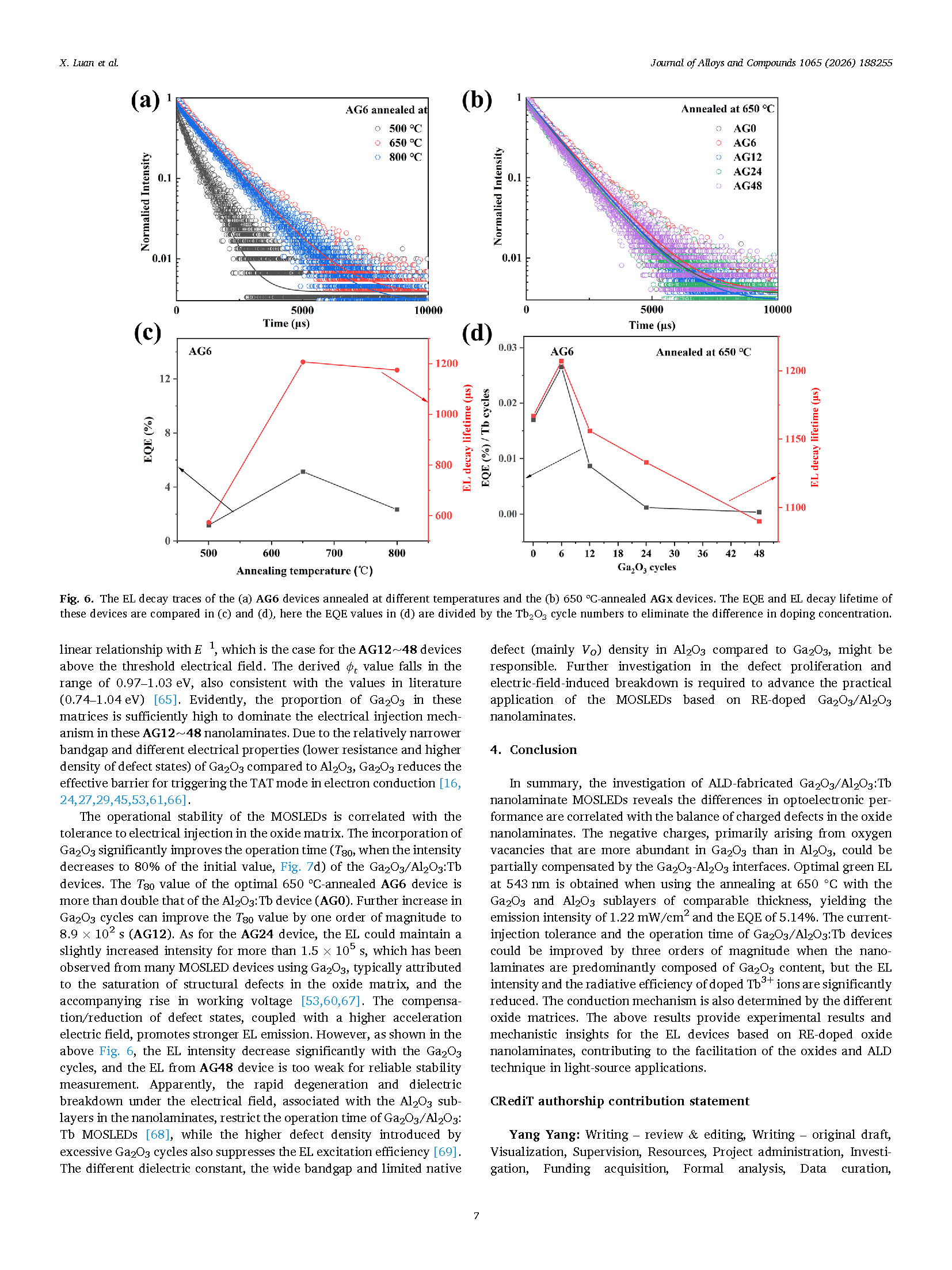
Figure 6 The EL decay traces of the (a) AG6 devices annealed at different temperatures and the (b) 650 ºC-annealed AGx devices. The EQE and EL decay lifetime of these devices are compared in (c) and (d), here the EQE values in (d) are divided by the Tb₂O₃ cycle numbers to eliminate the difference in doping concentration.
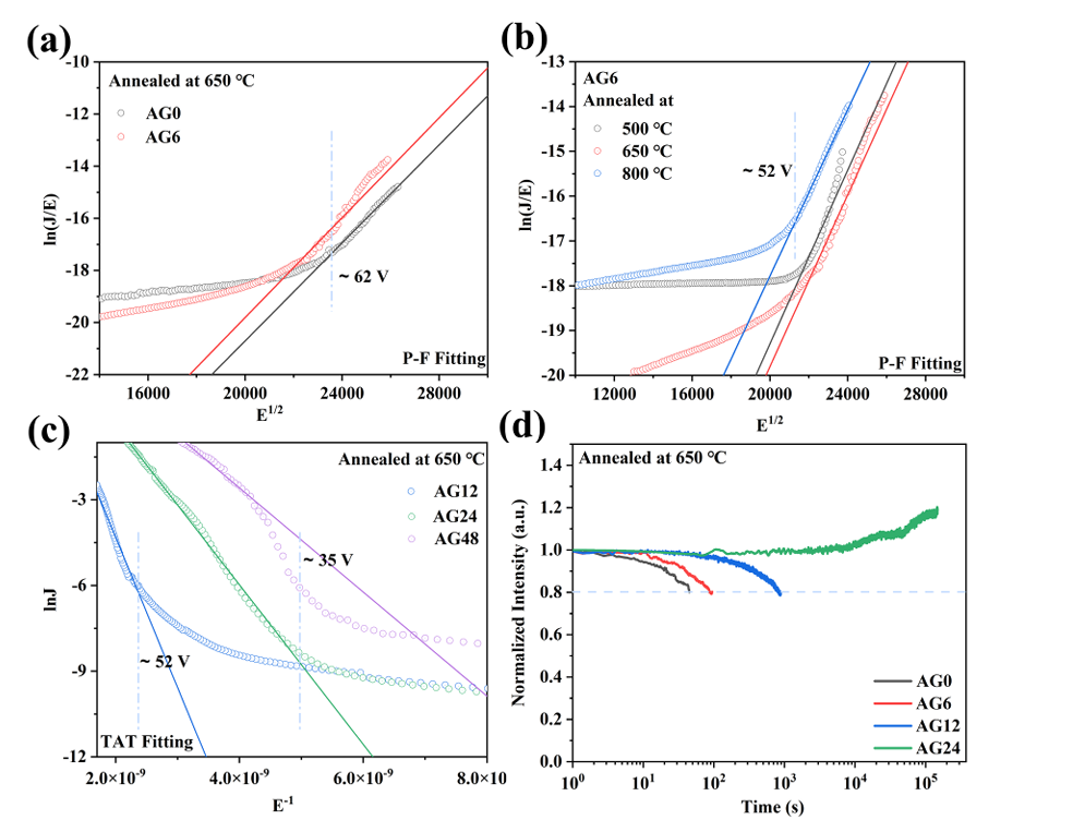
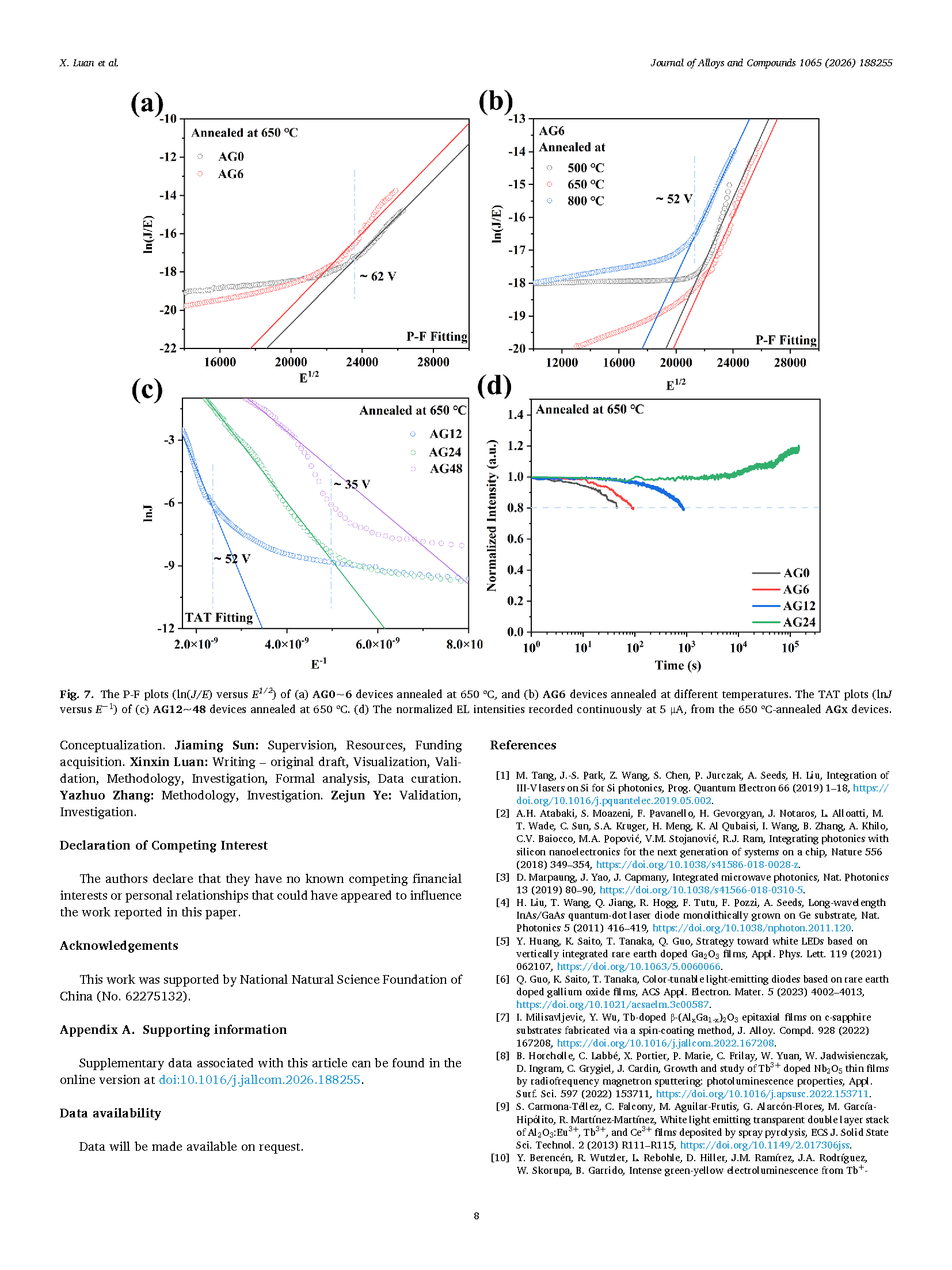
Figure 7 The P-F plots (ln(J/E) versus E¹ᐟ²) of (a) AG0~6 devices annealed at 650 ºC, and (b) AG6 devices annealed at different temperatures. The TAT plots (lnJ versus E⁻¹) of (c) AG12~48 devices annealed at 650 ºC. (d) The normalized EL intensities recorded continuously at 5 μA, from the 650 ºC-annealed AGx devices.
DOI:
10.1016/j.jallcom.2026.188255