Paper Sharing
【Member Papers】Enhancement of gallium oxide-based solar-blind photodetectors through comprehensive process optimization
日期:2026-05-29阅读:142
Researchers from the Xi'an University of Posts &Telecommunications have published a dissertation titled "Enhancement of gallium oxide-based solar-blind photodetectors through comprehensive process optimization" in Materials Science in Semiconductor Processing.
Background
Solar-blind ultraviolet (SBUV) detection technology has emerged as a research hotspot in optoelectronic detectors in recent years due to its irreplaceable advantages in missile early warning, flame detection, and space communication. Compared to conventional UV detectors (e.g., Si-based or GaN-based devices), SBUV detectors selectively respond to UV signals in the solar-blind spectral region (wavelength <280 nm), effectively eliminating solar radiation background noise and significantly improving signal-to-noise ratio (SNR) and detection accuracy. Among various candidate materials, gallium oxide (Ga2O3) stands out as an ideal material for next-generation SBUV detectors owing to its ultra-wide bandgap (4.9 eV), high breakdown electric field strength (8 MV/cm), excellent chemical stability, and potential for low-cost solution-based fabrication.
The performance of photodetectors, such as responsivity, response speed, and detectivity, is closely correlated with the fabrication process and device materials. Among these, annealing temperature and device structure are recognized as the core factors governing photoelectric conversion efficiency. On the one hand, annealing modulates the crystallinity, defect density, and electrode–film interfacial quality of gallium oxide thin films, thereby directly determining the generation and transport dynamics of photogenerated carriers, which reflects the intrinsic characteristics of the material. On the other hand, device structure dictates the transport path length and recombination probability of photocarriers, thus exerting a prominent influence on response speed and photocurrent amplitude, which characterizes the carrier transport behavior of the device.
Abstract
The high performance of solar-blind ultraviolet detectors is closely related to their manufacturing processes and device structures. However, existing research lacks an analysis of the comprehensive impact of these two aspects on performance. In this paper, significant improvements in device performance are achieved through precise temperature control in multi-step processes and optimization of the charge transport spacing within the device. In addition, the performance factor FOM3 is used to realize the unified quantitative evaluation of multiple performance indicators, enabling faster comparison of the comprehensive performance of devices. The results show that the device annealed at 500 °C exhibits the best comprehensive performance. Under 254 nm ultraviolet irradiation, it achieves a photo-to-dark current ratio of 9.56 × 10⁸, a responsivity of 3.97 × 10³ A/W, a detectivity of 3 × 10¹⁴ Jones, and an external quantum efficiency of 1.94 × 10⁴%, with the comprehensive performance factor FOM3 as high as 1.63 × 10¹³. Meanwhile, the response time of the device annealed at 900 °C is improved by nearly 40 times, which provides enlightenment for the optimal design and practical application of SBUV detectors.
Highlights
The effects of fabrication processes and device structures are investigated to optimize the performance of photodetectors.
The annealing temperature affects the crystallinity and oxygen vacancy concentration of Ga2O3 thin films.
Reducing the interdigital electrode spacing shortens the carrier transport distance, which can enhance the photocurrent.
The FOM3 is used to quantify the balance of sensitivity, energy conversion efficiency and response speed.
Conclusion
In this work, high-performance Ga2O3 solar-blind photodetectors were fabricated using ALD.
The effects of annealing temperature and electrode spacing on device performance and crystallinity were systematically studied. It was found that the Ga2O3 thin film annealed at 500 °C has optimal oxygen vacancy concentration and surface flatness, which can significantly improve carrier concentration and interface contact quality. As a result, the device exhibits more excellent comprehensive performance under 254 nm ultraviolet irradiation: the PDCR reaches 9.56 × 10⁸ , the D* is 3 × 10¹⁴ Jones, the EQE is as high as 1.94 × 10⁴ %, and the R reaches 3.97 × 10³ A/W. By proposing the comprehensive performance factor FOM3, the multi-dimensional performance advantages of the device in sensitivity, conversion efficiency, and response speed were quantitatively evaluated. Data analysis shows that the device annealed at 500 °C achieves a balance between high responsivity and low dark current by regulating the crystallinity and defect state distribution of the thin film, thus having the highest comprehensive performance. In contrast, the device annealed at 900 °C achieves nearly a 40-fold improvement in response time due to the optimized oxygen vacancy concentration. The results of this study not only provide an important reference for the development of high-performance Ga2O3 solar-blind ultraviolet detectors but also offer new ideas for the process optimization and performance evaluation of wide-bandgap semiconductor optoelectronic devices.
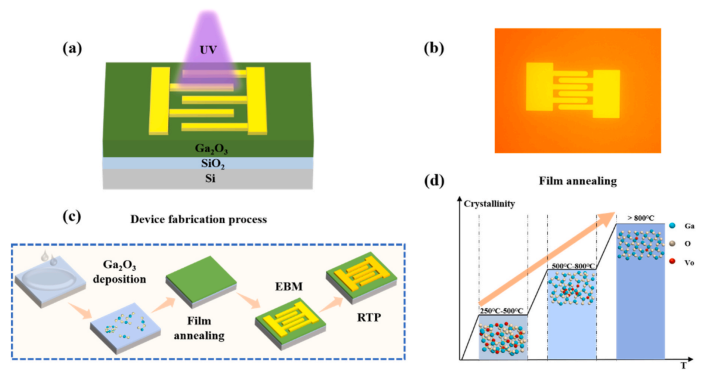
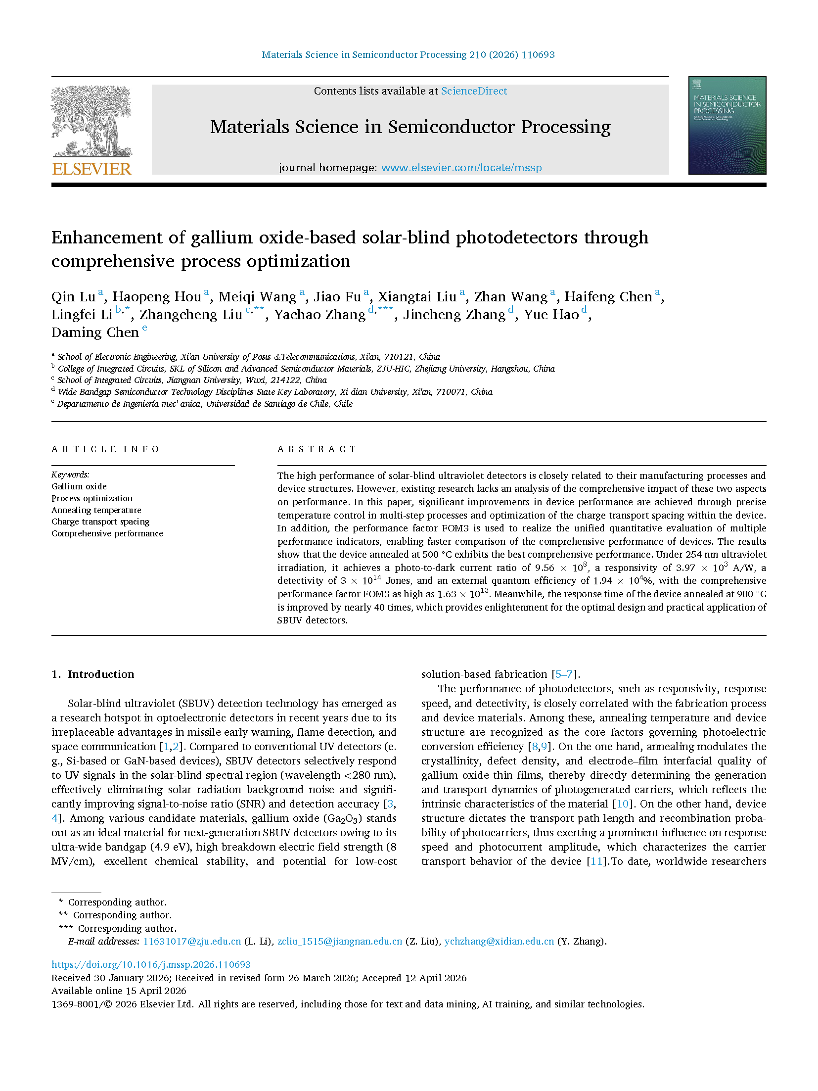
Fig. 1. (a)Schematic illustration of the device working mechanism, (b) Optical photograph of the device; (c) Fabrication process of the device, (d) Effect of different annealing temperatures on crystallinity.
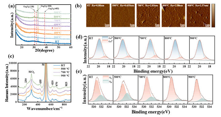
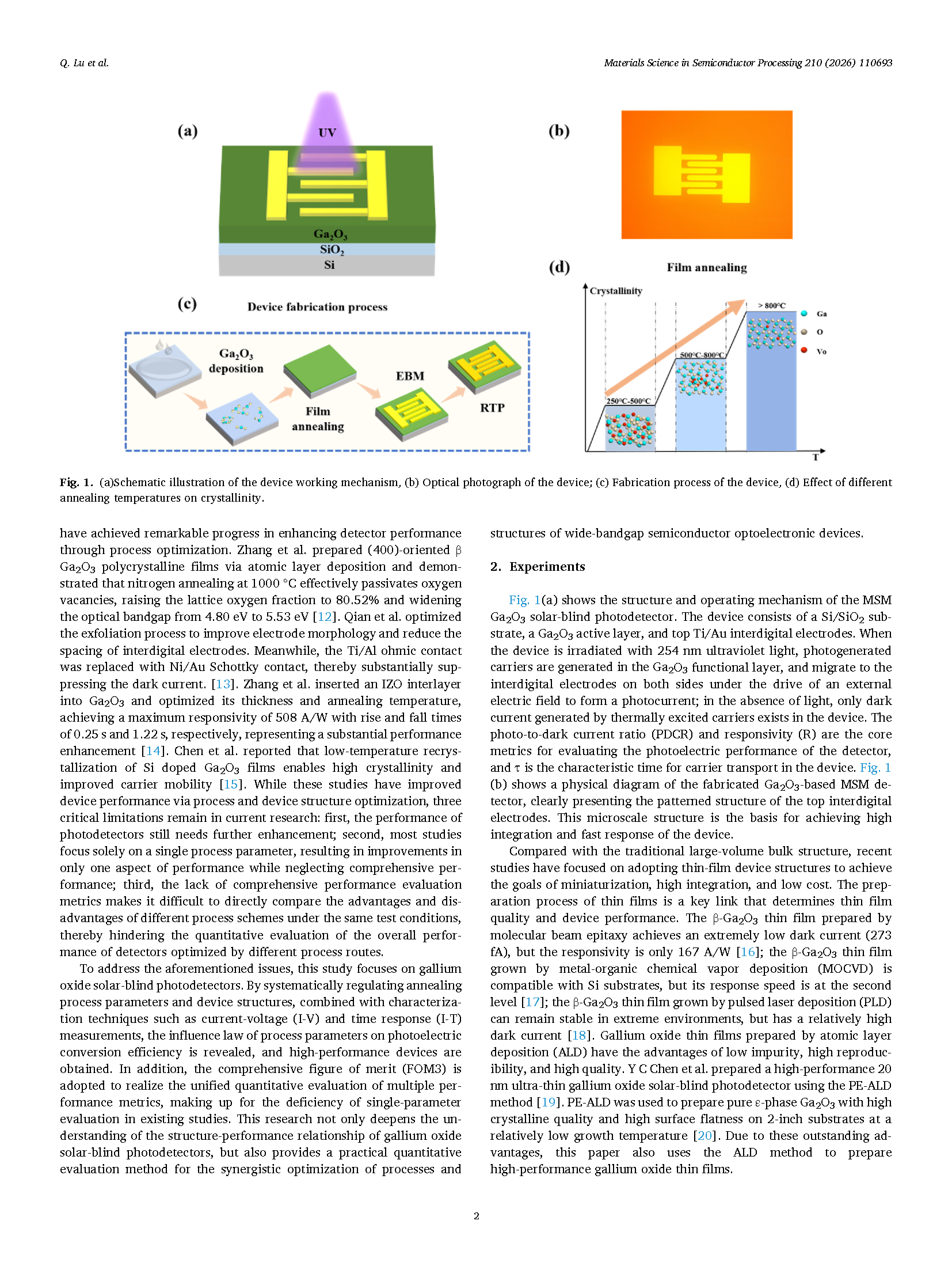
Fig. 2. (a) XRD patterns, (b) AFM images, (c) Raman spectra, (d) Ga 3d X-ray photoelectron spectroscopy, (e) O 1s X-ray photoelectron spectroscopy.
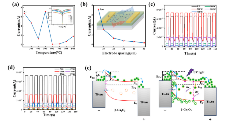
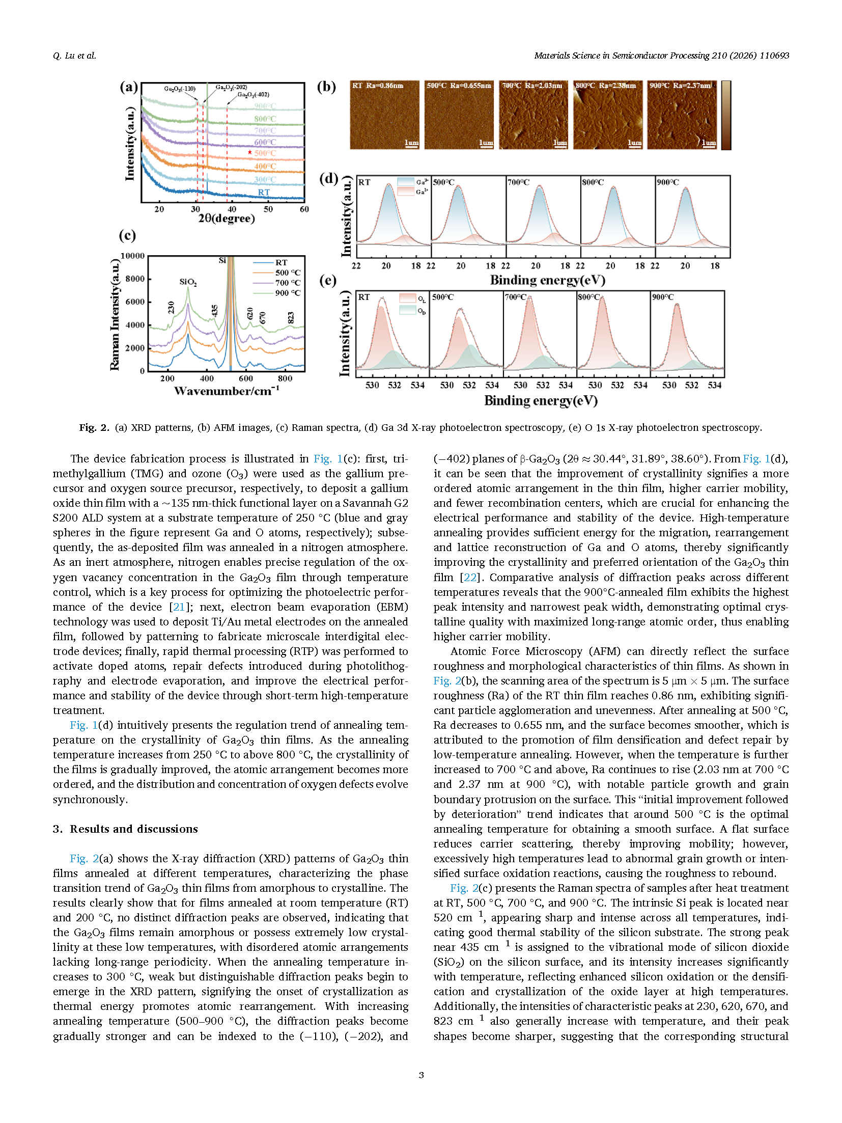
Fig. 3. (a) Photocurrent at different temperatures under 5V current (the inset shows the photocurrent at different annealing temperatures with a spacing of 5 μm), (b) Photocurrent at different device electrode spacings under 5V current, (c) I-T characteristics at a 5 μm spacing under different annealing temperatures, (d) I-T characteristics at different interdigitated electrode spacings, (e) Schematic diagram.
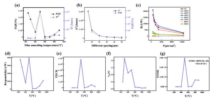
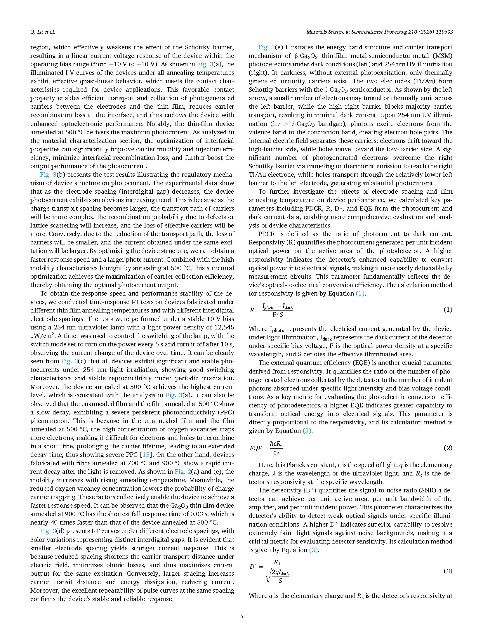
Fig. 4. (a) EQE and D* of thin-film devices with 5 μm electrode spacing under different annealing temperatures, (b) EQE and D* of the thin film at 500 °C annealing temperature with varying electrode spacings, (c) R as a function of light power density under different annealing temperatures, (d) R of devices with 5 μm electrode spacing under different annealing temperatures, (e) Photoconductive gain × detectivity under different annealing temperatures, (f) Decay time (τd) as a function of annealing temperature, (g) FOM3 as a function of annealing temperature.
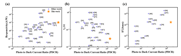
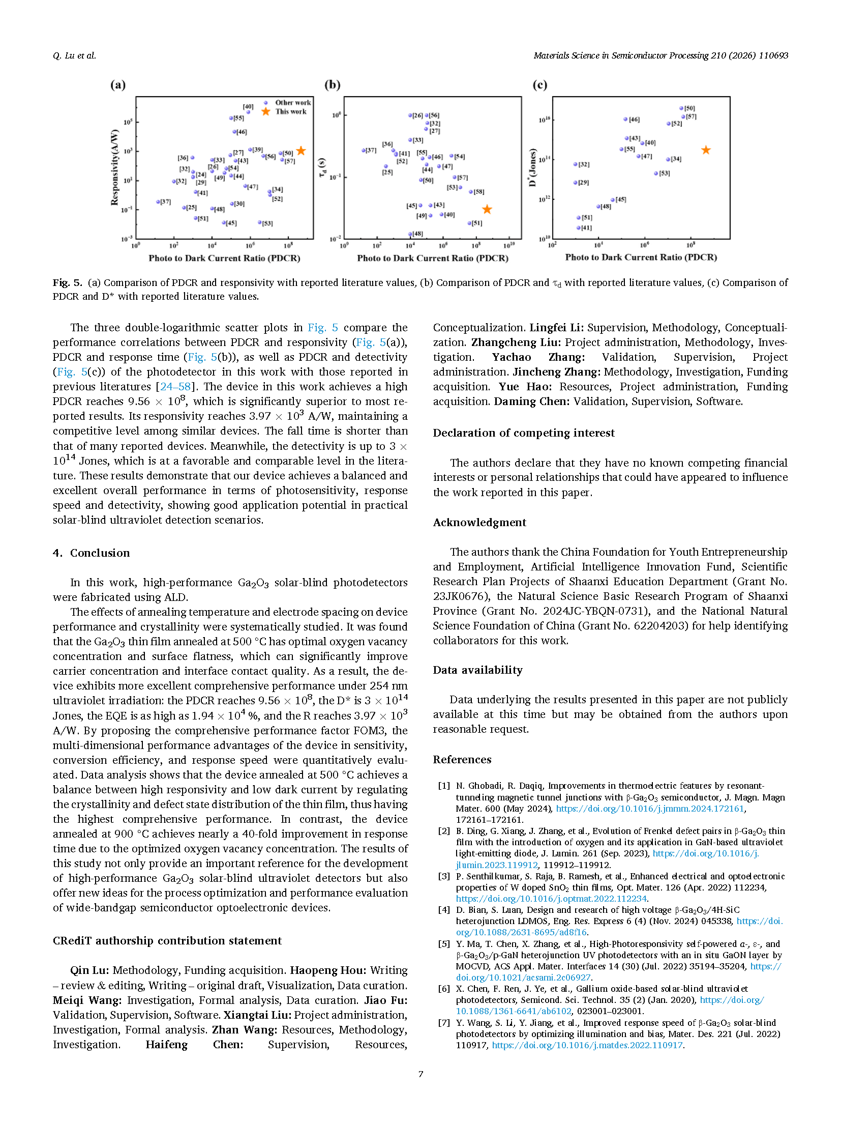
Fig. 5. (a) Comparison of PDCR and responsivity with reported literature values, (b) Comparison of PDCR and τd with reported literature values, (c) Comparison of PDCR and D* with reported literature values.
DOI:
doi.org/10.1016/j.mssp.2026.110693