Paper Sharing
【Domestic Papers】Step-by-Step Shouldering Growth of (100) β-Ga₂O₃ with Large Thickness
日期:2026-06-02阅读:109
Researchers from the Shanghai Institute of Optics and Fine Mechanics, Chinese Academy of Sciences have published a dissertation titled "Step-by-Step Shouldering Growth of (100) β‑Ga₂O₃ with Large Thickness" in Crystal Growth & Design.
Background
β‑Ga₂O₃ is an emerging ultrawide bandgap semiconductor with a bandgap of 4.8 eV, a breakdown electric field strength of 8 MV/cm, and excellent thermal/chemical stability. It has broad prospects in high‑power devices and deep‑ultraviolet photodetectors, with lower fabrication costs than SiC and GaN. The EFG method is the mainstream approach for growing large‑size β‑Ga₂O₃. The (100) plane has low surface energy and facilitates large‑size single crystals but is difficult for epitaxy. Conventional EFG‑grown (100) β‑Ga₂O₃ crystals are too thin; simultaneous 2D shouldering in thickness and width easily causes miscellaneous crystals and twins due to distinct growth habits, hindering large‑thickness growth.
Abstract
β‑Ga₂O₃ crystals are anisotropic, which is also reflected in their growth habits. This is manifested in the occurrence of phenomena such as miscellaneous crystals and twin crystals due to the competition between different crystal planes, which affects the growth of large sizes. However, this anisotropic growth is not all a drawback; instead, it can be utilized to achieve the growth of specific crystal planes. In this article, by analyzing the growth dynamics mechanism of different crystal planes of β‑Ga₂O₃, we qualitatively determined the suitable growth intervals for different crystal planes, and actively designed the thermal field and growth process that meet the requirements, successfully achieving the expected results. We conducted phased control over the shoulder expansion of (100) plane, obtaining high‑quality β‑Ga₂O₃ single crystals.
Highlights
Based on the kinetic difference that the (100) plane is a smooth interface and other planes are rough interfaces, a step‑by‑step shouldering strategy is proposed: first grow a thin layer along the die length, then expand to the full die surface in the thickness direction.
The thermal field is optimized by adding an iridium heating ring and cover outside the crucible, realizing precise control of undercooling at the growth interface and suppressing miscellaneous crystals.
Large‑thickness (100) β‑Ga₂O₃ single crystals are successfully fabricated, with the equaldiameter section thickness exceeding 10 mm and excellent crystalline quality.
Conclusion
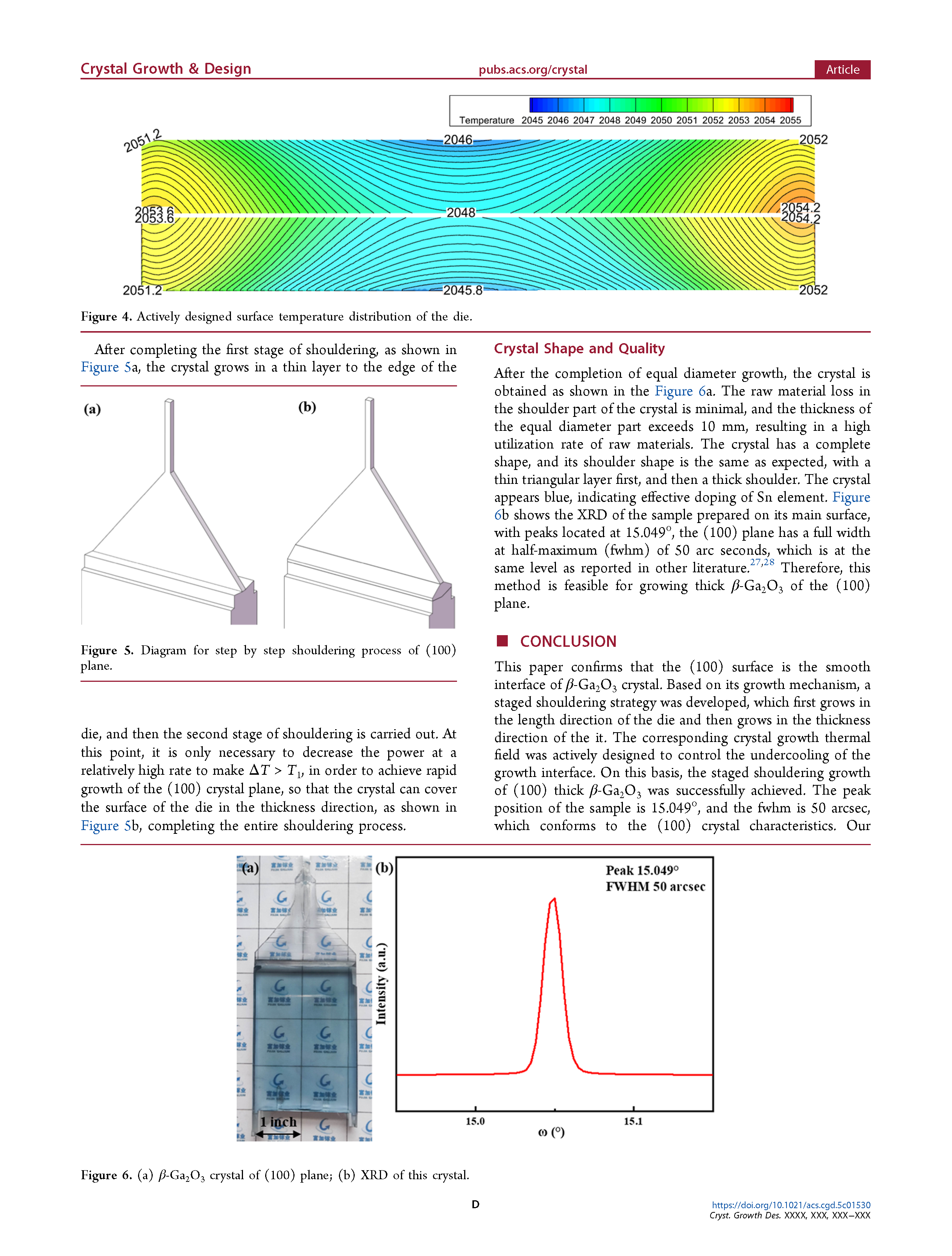
This paper confirms that the (100) surface is the smooth interface of β‑Ga₂O₃ crystal. Based on its growth mechanism, a staged shouldering strategy was developed, which first grows in the length direction of the die and then grows in the thickness direction of the it. The corresponding crystal growth thermal field was actively designed to control the undercooling of the growth interface. On this basis, the staged shouldering growth of (100) thick β‑Ga₂O₃ was successfully achieved. The peak position of the sample is 15.049°, and the fwhm is 50 arcsec, which conforms to the (100) crystal characteristics. Our research provides an alternative perspective for designing the growth of β‑Ga₂O₃ crystal.
Project Support
The study was supported by Research on Key Technologies of 4‑in. Gallium Oxide Materials and Devices (grant number 23511102300). We gratefully acknowledge Hangzhou Fujia Gallium Technology Co., Ltd. for providing grown crystal and processing.
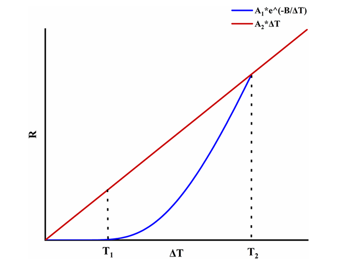
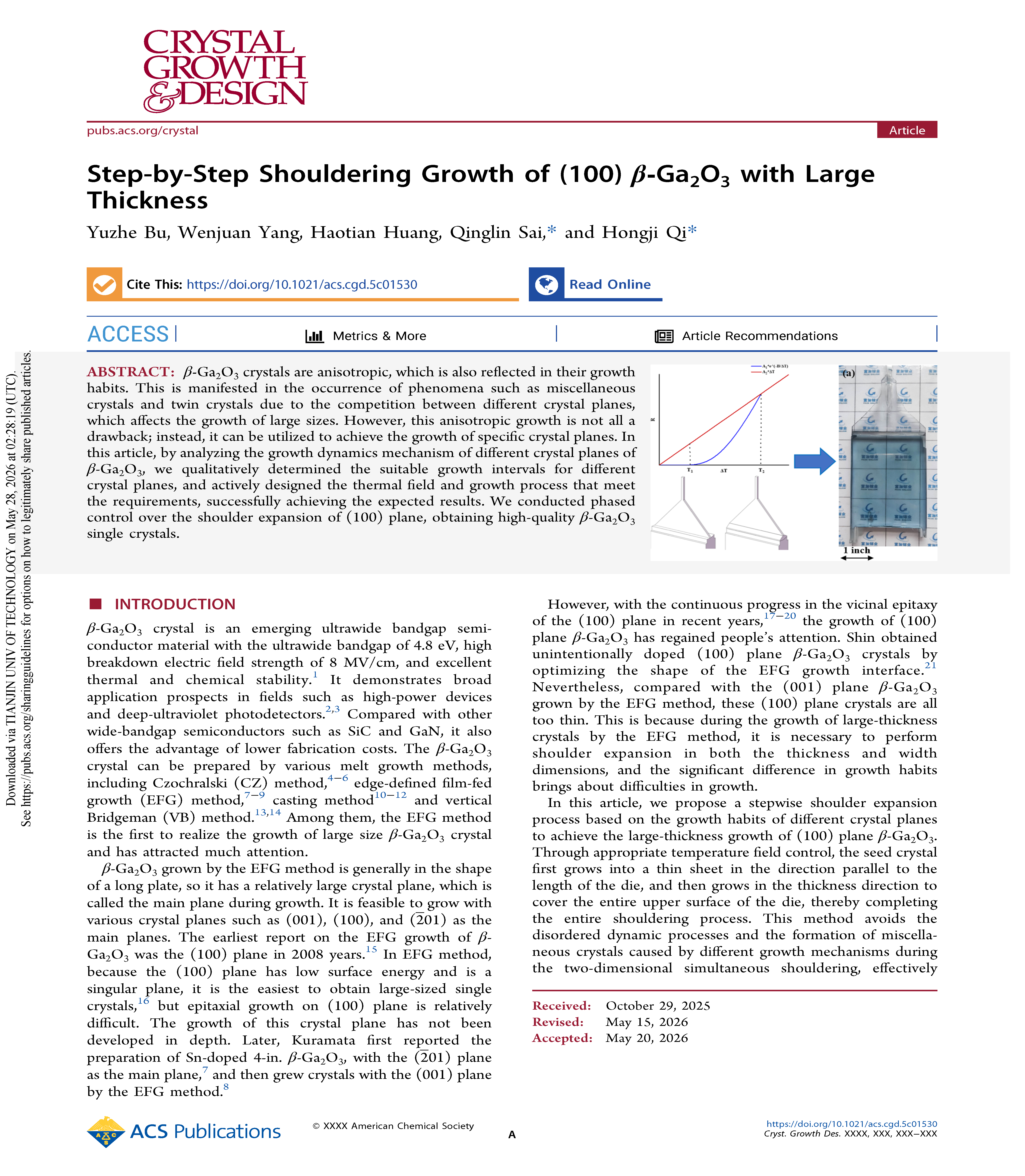
Figure 1 Growth rate R as a function of undercooling ΔT
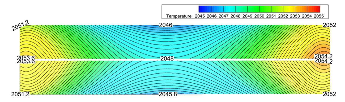
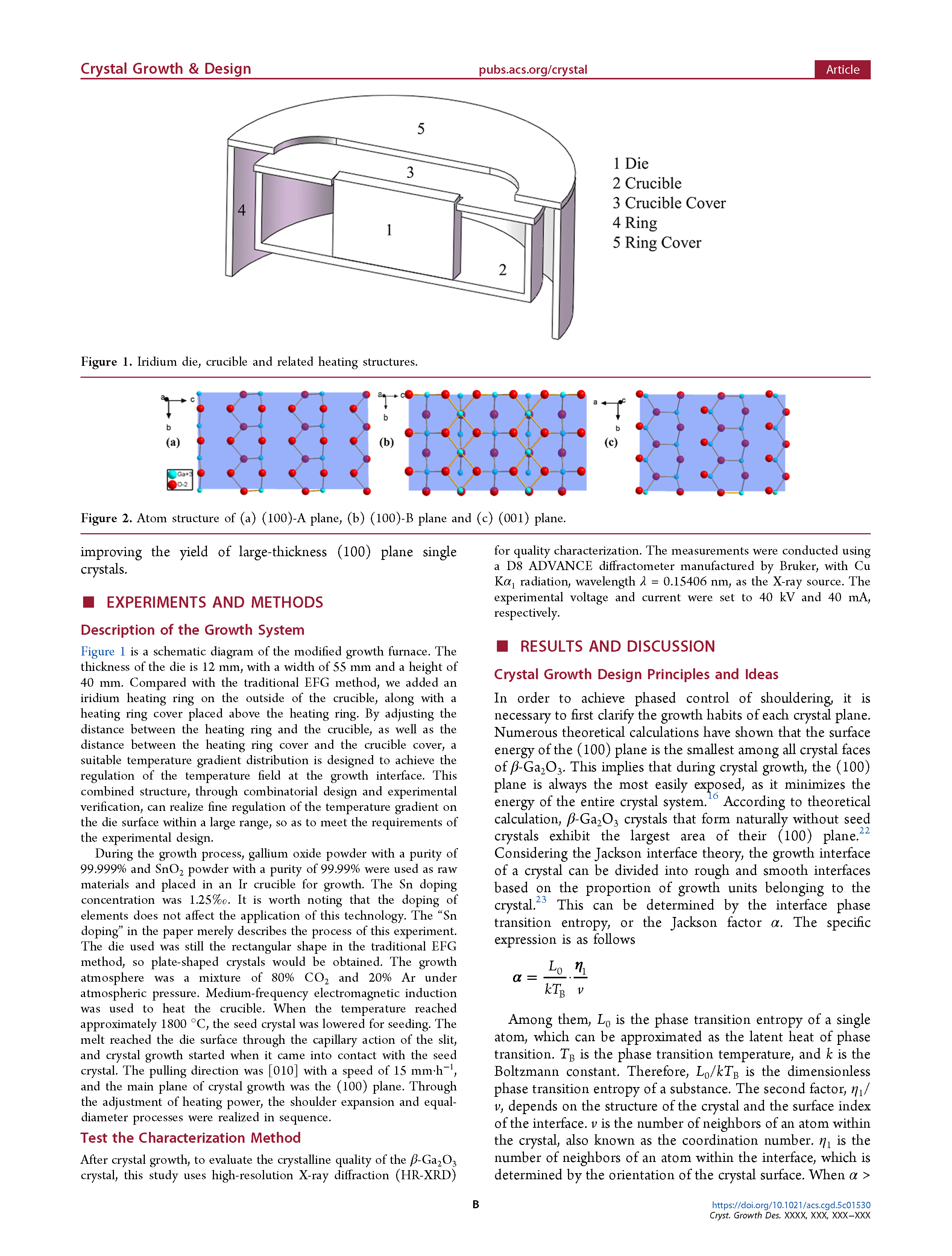
Figure 2 Actively designed surface temperature distribution of the die.
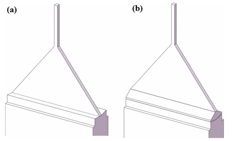
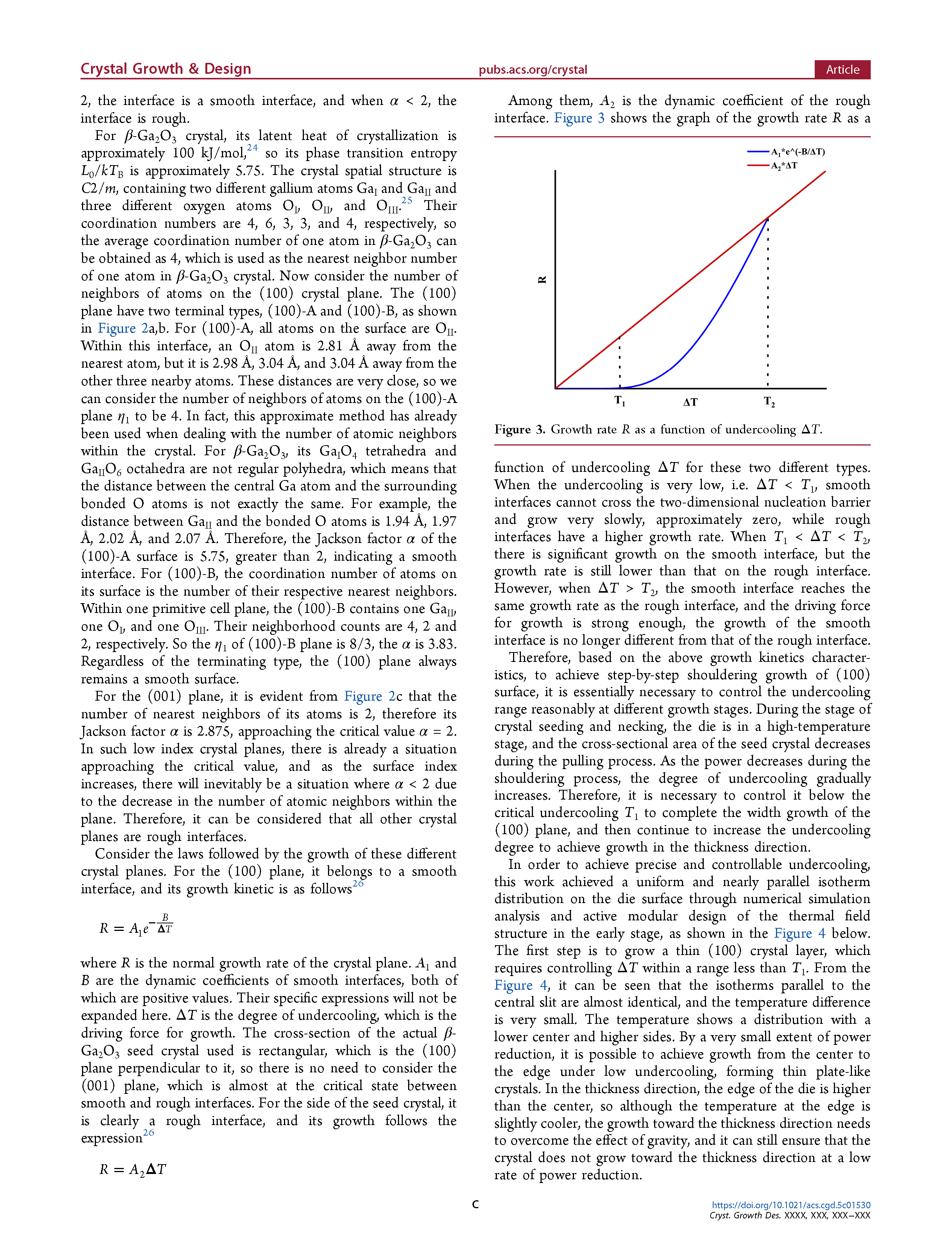
Figure 3 Diagram for step by step shouldering process of (100) plane.
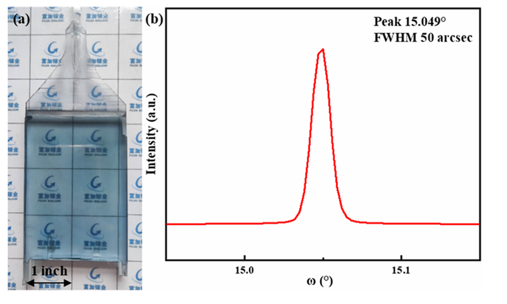
Figure 4 (a) β-Ga₂O₃ crystal of (100) plane; (b) XRD of this crystal.
DOI:
doi.org/10.1021/acs.cgd.5c01530