Paper Sharing
【Member Papers】Recent advances in diamond-gallium oxide heterojunction photodetectors: a review of emerging technologies
日期:2026-06-12阅读:84
Researchers from the Hunan University have published a dissertation titled "Recent advances in diamond-gallium oxide heterojunction photodetectors: a review of emerging technologies" in Semiconductor Science and Technology.
Background
Deep-ultraviolet (DUV, 200–280 nm) photodetectors have irreplaceable advantages in ozone monitoring, missile tracking, flame detection, UV communication, biomedical detection, etc. As an ultra-wide bandgap semiconductor (5.5 eV), diamond has ultra-high thermal conductivity, high chemical stability, high breakdown voltage, etc., but its detection wavelength is only below 225 nm, with complex preparation and high cost. Gallium oxide (Ga₂O₃, ~4.9 eV) covers the solar-blind UV region, with accessible large-size single crystals and mature fabrication, but suffers from low thermal conductivity, low carrier mobility, and difficulty in effective p-type doping. To break through bottlenecks of single materials, diamond/Ga₂O₃ heterojunctions have become a research hotspot for high-performance DUV photodetectors due to matched bandgaps, good thermal/chemical compatibility, and complementary p-n conductivity.
Abstract
A novel wide-bandgap semiconductor heterostructure, diamond/gallium oxide (Ga₂O₃), demonstrates significant potential in the fields of optoelectronic devices, power electronic devices, and radiation detection. The synergistic combination of the materials’ outstanding features, including diamond’s relatively mature p-type doping technology and exceptional thermal conductivity, along with Ga₂O₃’s n-type conductivity and broad ultraviolet (UV) spectral response range, enhances the performance and application scope of photodetectors. This review presents recent advancements in diamond/Ga₂O₃ heterojunction devices, covering progress in band engineering, interface design, and strategies for optimizing device performance. Furthermore, it analyzes potential applications of diamond/Ga₂O₃ photodetectors in imaging systems, self-powered sensing, and extreme environment monitoring. Future research prioritizes interface passivation, defect engineering, and scalable fabrication techniques to facilitate the practical application of this material system in deep UV photonics and intelligent sensing technologies.
Highlights
Propose heterojunction design with complementary advantages of diamond and Ga₂O₃ to achieve near-full-spectrum DUV detection (200–280 nm).
Use ultra-high thermal conductivity of diamond to mitigate self-heating effect of Ga₂O₃ and improve device high-temperature stability and reliability.
Use p-type diamond to compensate for the difficulty of p-type doping in Ga₂O₃ and construct high-efficiency p-n heterojunction and built-in electric field.
Develop interface optimization, doping modulation, van der Waals integration and other strategies to significantly improve responsivity, PDCR and response speed.
Realize multi-functional applications including self-powered detection, solar-blind imaging, position detection and high-temperature operation.
Conclusion
The diamond/Ga₂O₃ heterostructure photodetectors exhibit significant potential in the domain of DUV photodetection, which is attributed to their exceptional properties. By integrating the advantages of both materials--diamond's high thermal conductivity and p-type doping capabilities, alongside Ga₂O₃'s responsiveness to high-energy photons and n-type conductivity--this heterojunction device demonstrates a markedly enhanced capacity for UV light detection. The heterojunction effectively detects full-spectrum or near-full-spectrum DUV light while maintaining excellent performance under elevated temperature conditions. Consequently, it represents a promising candidate for the advancement of high-performance DUV photodetectors. Despite these advancements, several critical challenges persist in the further development of diamond/Ga₂O₃ heterojunction photodetectors. The key issues include the necessity for optimized interface passivation and defect engineering to reduce interface state density and defect-related currents, which are essential for enhancing device stability and reliability. Furthermore, the scalable fabrication of high-quality, large-area materials continues to pose a significant obstacle. Future research should concentrate on the following key directions: (1) the formulation of innovative interface engineering strategies, such as the incorporation of buffer layers or interface modification techniques, to improve interface bonding and charge transport properties; (2) the investigation of novel doping techniques to optimize conductivity and achieve better carrier concentration matching between diamond and Ga₂O₃; and (3) the establishment of efficient and cost-effective material fabrication processes to support industrial applications. Research on diamond/Ga₂O₃ heterojunctions continues, while the search for alternative p-type materials gains significance in advancing Ga₂O₃-based heterojunction photodetectors. Due to the high cost and complexity of p-type diamond, wide-bandgap p-type semiconductors like p-GaN, p-SiC, and p-type oxide semiconductors (NiO-, CuO-, and Cu₂O-based materials) are poised to be practical and scalable replacements for in-depth studies. These materials offer valuable insights into interfacial band alignment, defect engineering, and carrier transport regulation in Ga₂O₃ heterojunction devices, guiding the optimization of diamond/Ga₂O₃ heterojunction photodetectors and their large-scale deployment. In conclusion, diamond/Ga₂O₃ heterojunction photodetectors possess substantial research value and application potential in the domains of DUV photodetectors and intelligent sensing technologies. Through interface design, material optimization, and innovation in device structure, future advancements enable the development of a high-performance DUV photodetector. These advancements establish a robust foundation for practical applications in extreme environment monitoring, self-powered sensing, and intelligent imaging systems.
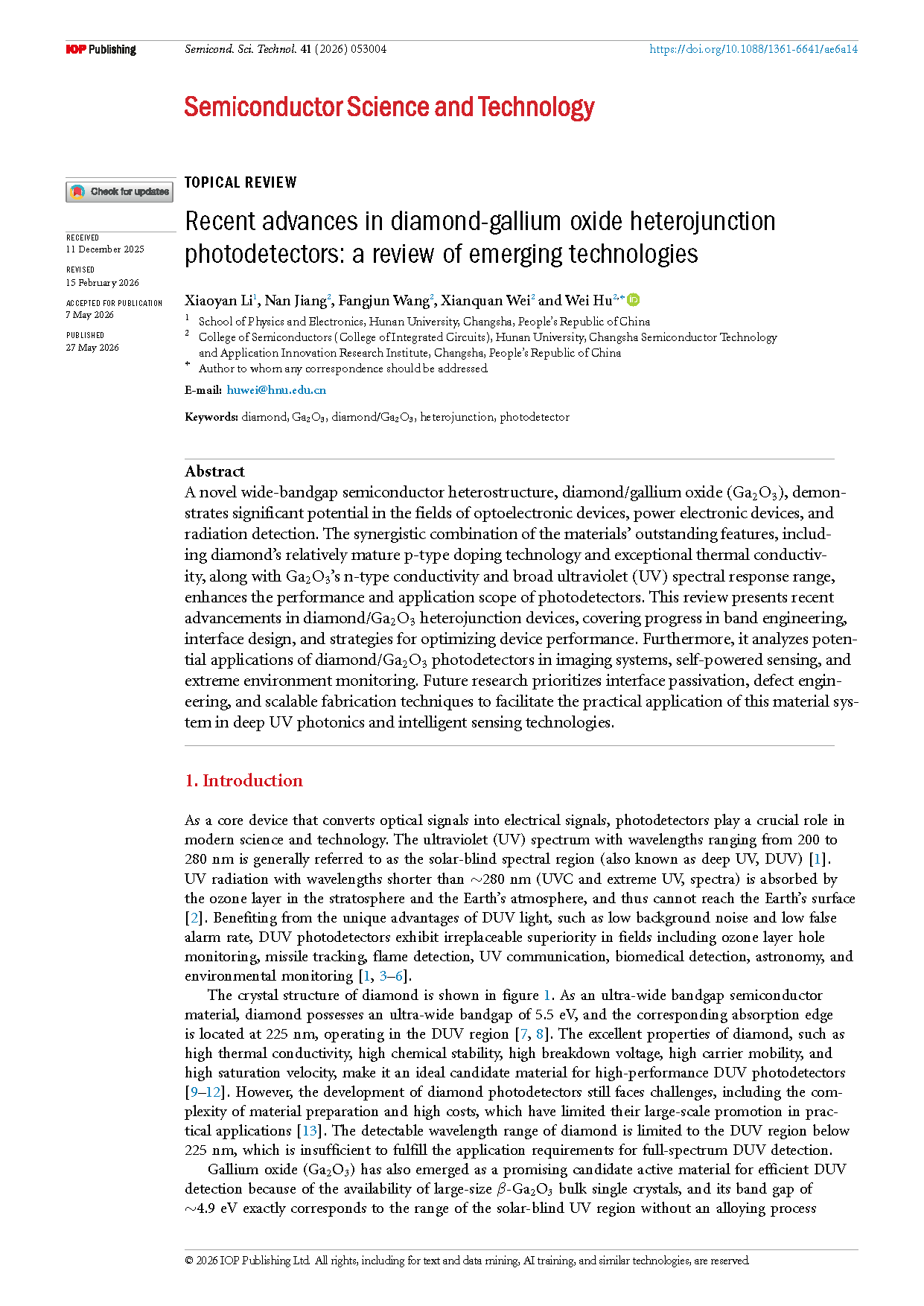
Figure 1 Schematic diagram of a diamond.
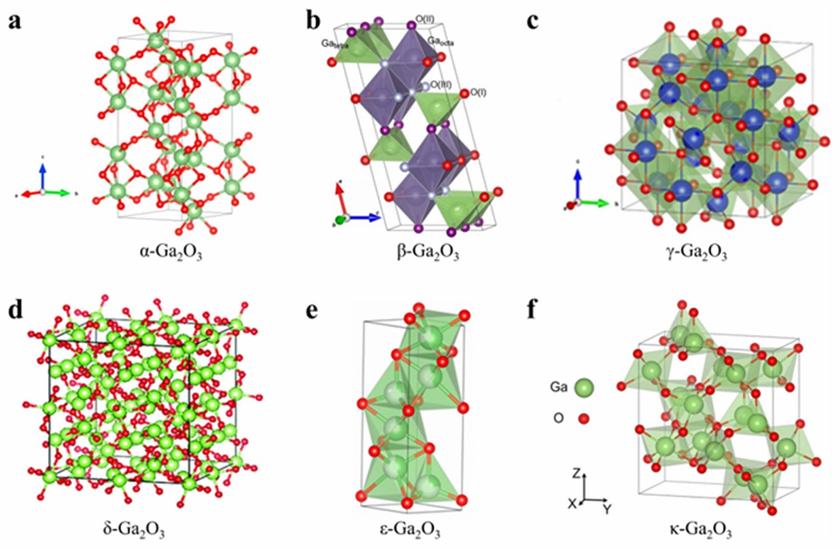
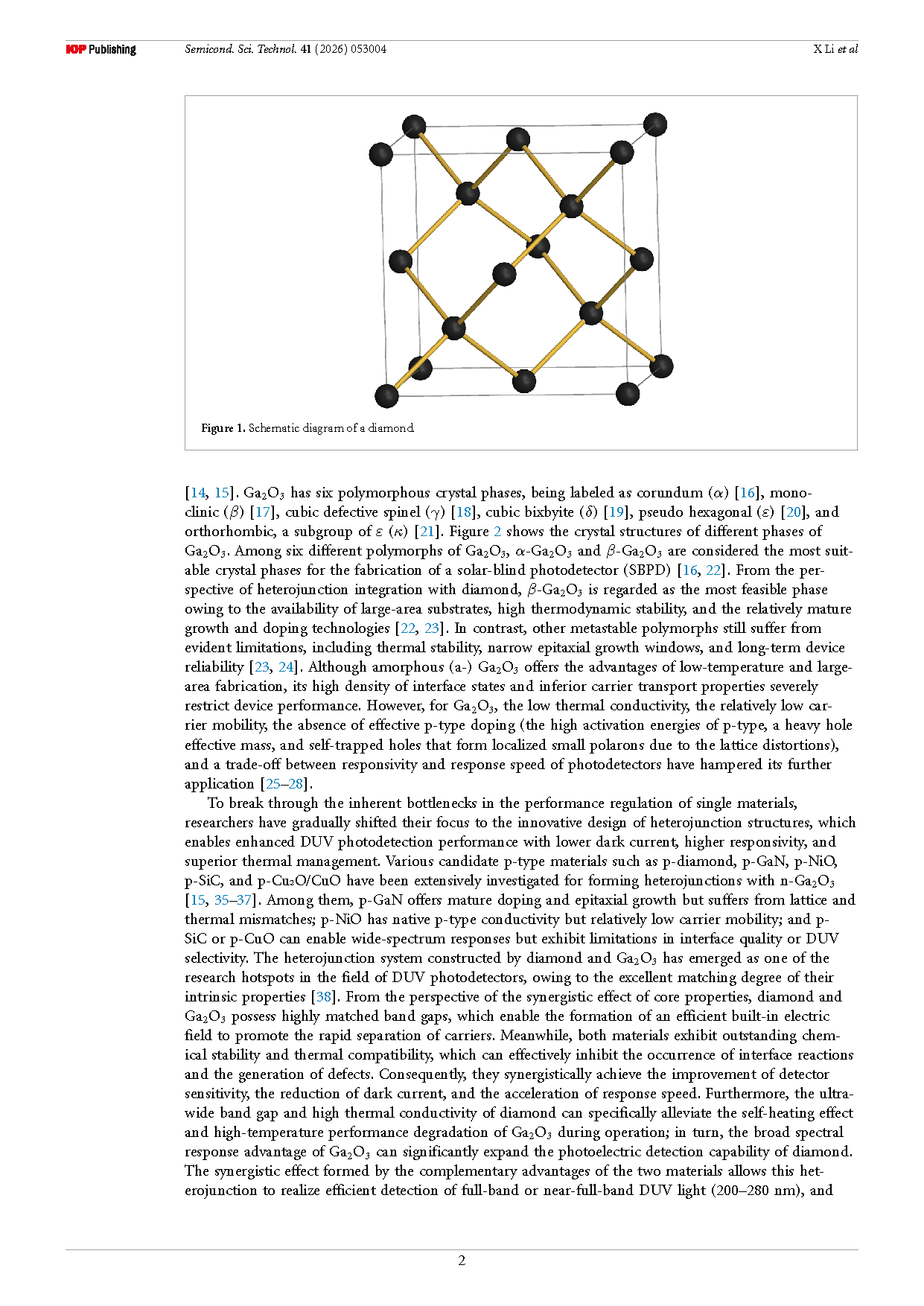
Figure 2 Schematic diagram of six phase structures: (a) α‑Ga₂O₃. (b) β‑Ga₂O₃. (c) γ‑Ga₂O₃. (d) δ‑Ga₂O₃.(e) ε‑Ga₂O₃. (f) κ‑Ga₂O₃.
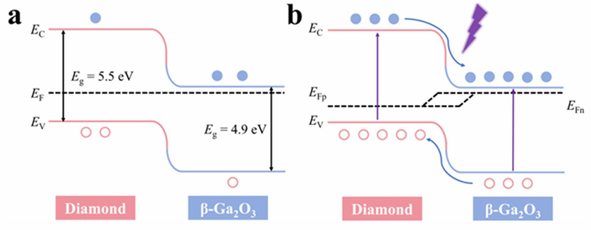
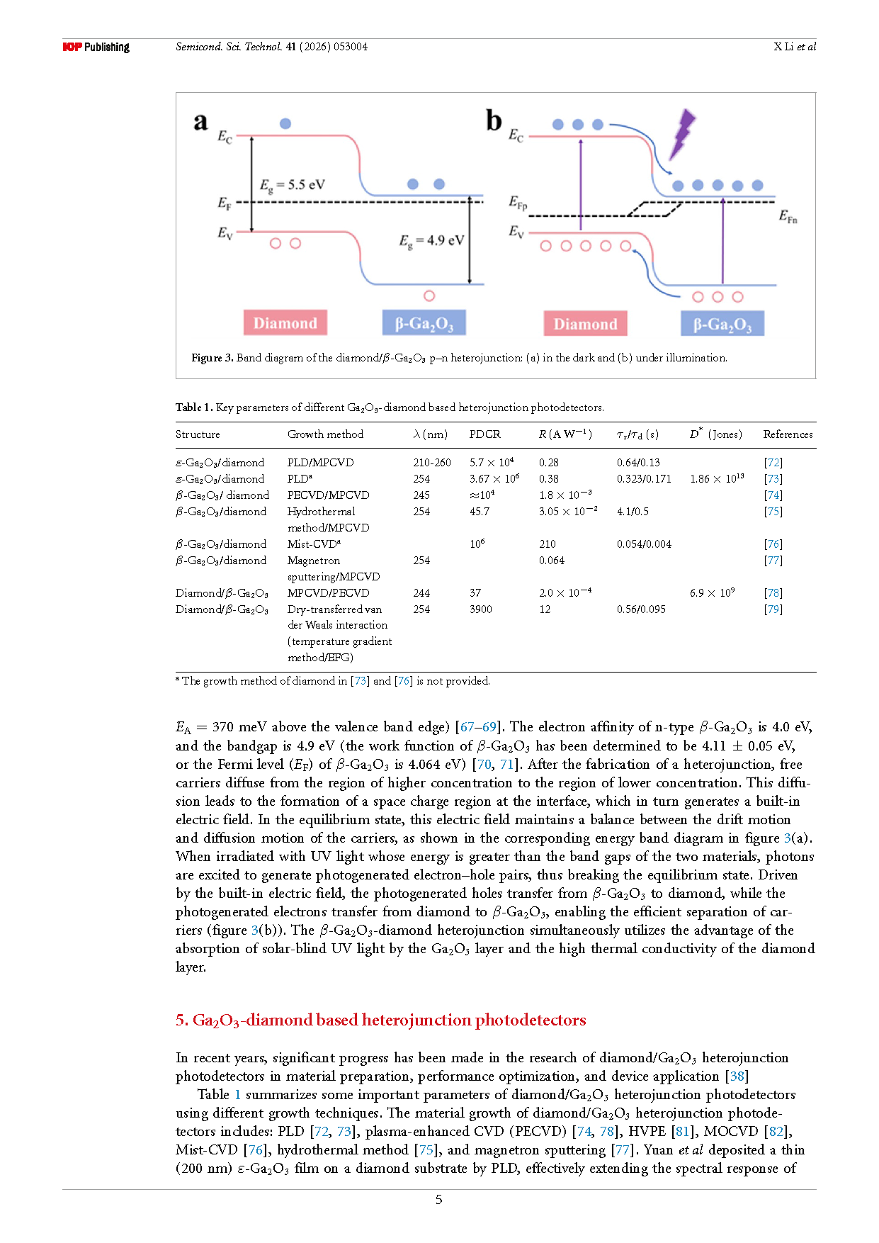
Figure 3 Band diagram of the diamond/β‑Ga₂O₃ p–n heterojunction: (a) in the dark and (b) under illumination.
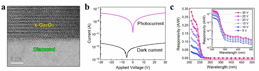
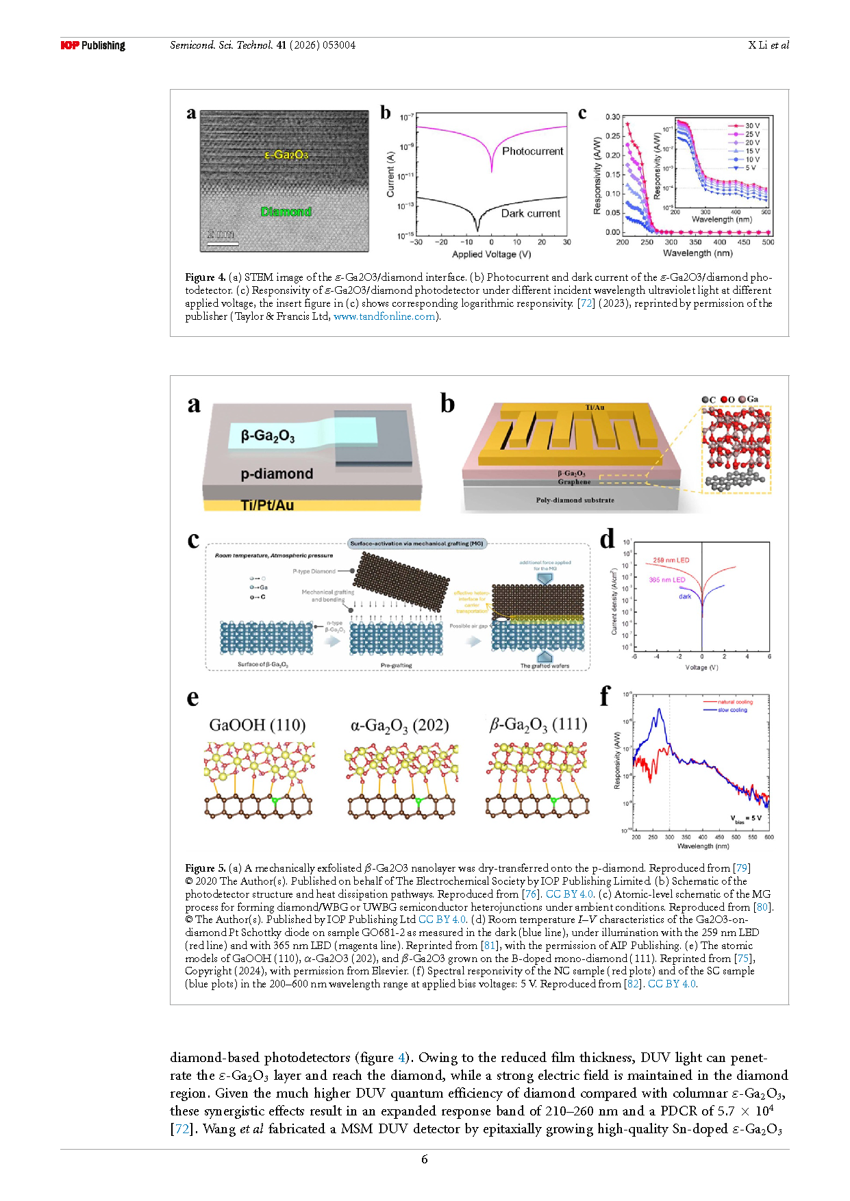
Figure 4 (a) STEM image of the ε‑Ga₂O₃/diamond interface. (b) Photocurrent and dark current of the ε‑Ga₂O₃/diamond photodetector. (c) Responsivity of ε‑Ga₂O₃/diamond photodetector under different incident wavelength ultraviolet light at different applied voltage, the insert figure in (c) shows corresponding logarithmic responsivity.
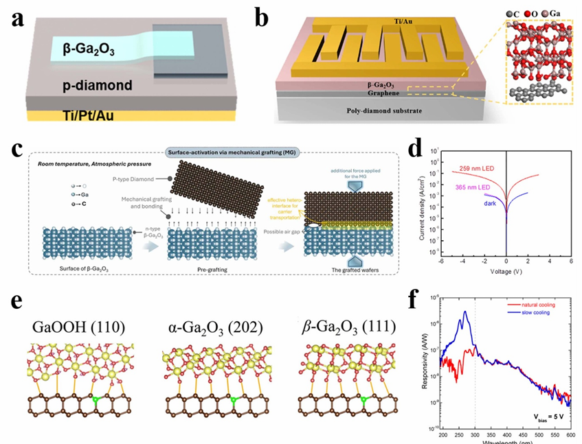
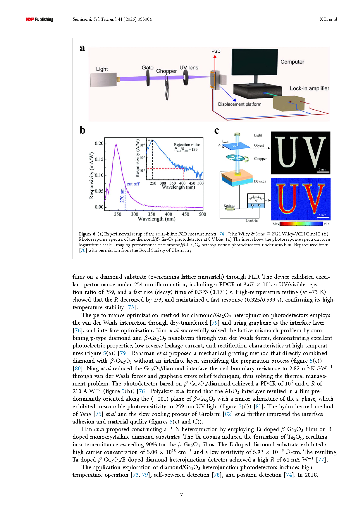
Figure 5 (a) A mechanically exfoliated β‑Ga₂O₃ nanolayer was dry‑transferred onto the p‑diamond. (b) Schematic of the photodetector structure and heat dissipation pathways. (c) Atomic‑level schematic of the MG process for forming diamond/WBG or UWBG semiconductor heterojunctions under ambient conditions. (d) Room temperature I–V characteristics of the Ga₂O₃‑ondiamond Pt Schottky diode on sample GO681‑2 as measured in the dark (blue line), under illumination with the 259 nm LED (red line) and with 365 nm LED (magenta line). (e) The atomic models of GaOOH (110), α‑Ga₂O₃ (202), and β‑Ga₂O₃ grown on the B‑doped mono‑diamond (111). (f) Spectral responsivity of the NC sample (red plots) and of the SC sample (blue plots) in the 200–600 wavelength range at applied bias voltages: 5 V.
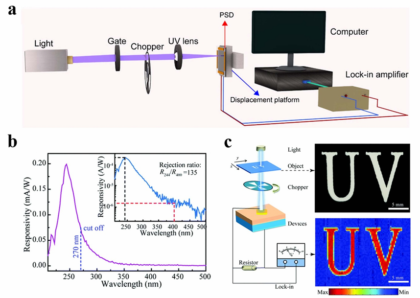
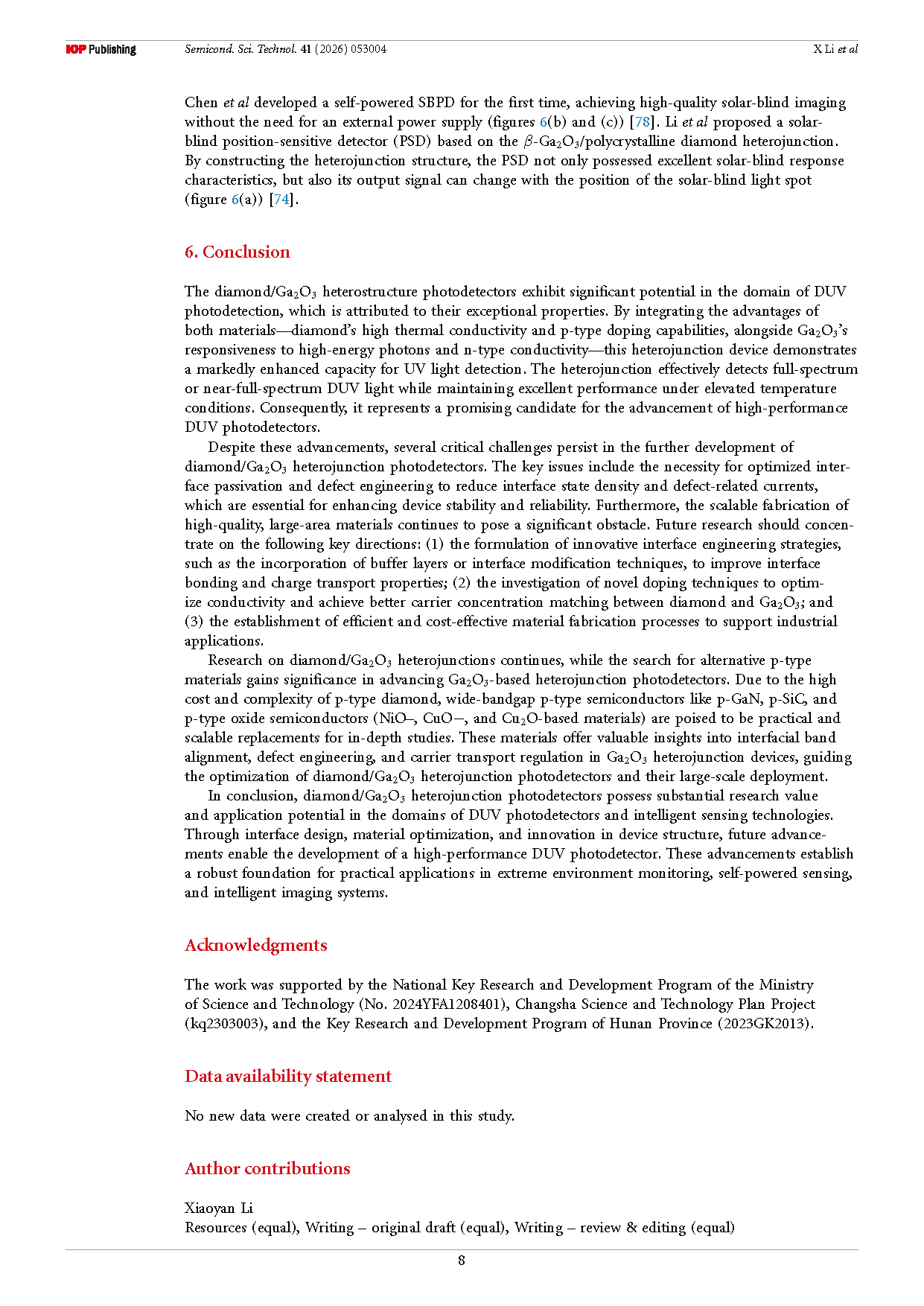
Figure 6 (a) Experimental setup of the solar‑blind PSD measurements. (b) Photoresponse spectra of the diamond/β‑Ga₂O₃ photodetector at 0 V bias. (c) The inset shows the photoresponse spectrum on a logarithmic scale. Imaging performance of diamond/β‑Ga₂O₃ heterojunction photodetectors under zero bias.
DOI:
doi.org/10.1088/1361-6641/ae6a14