


Discover
【Knowledge Discover】Why Can Gallium Oxide Enable Large-Area Substrates? A Look into Melt Growth Technology
日期:2026-06-14阅读:71
Introduction
In the previous installment of this series, we explored the crystal structure, material properties, and power electronics potential of gallium oxide. As a representative ultra-wide bandgap semiconductor, β-Ga₂O₃ features a bandgap of approximately 4.8–4.9 eV, a high critical breakdown field of around 8 MV/cm, and an outstanding Baliga figure of merit, making it one of the most promising candidates for next-generation high-voltage, low-loss power devices.
However, the industrialization of a semiconductor material depends on more than its intrinsic properties alone. For power electronics, the availability of large-area, high-quality, and cost-effective single-crystal substrates is often a decisive factor in determining whether a material system can achieve large-scale commercial adoption. Compared with SiC and GaN, one of the most distinctive advantages of β-Ga₂O₃ is that large-size single-crystal substrates can be grown using relatively mature melt-growth techniques. This capability sets β-Ga₂O₃ apart from many other wide-bandgap semiconductor materials and represents a key advantage for its industrial development.
In this article, we focus on the melt growth of β-Ga₂O₃ single-crystal substrates. We begin by examining why β-Ga₂O₃ is particularly well suited for melt-growth methods, and then introduce the major crystal growth technologies, including the Floating Zone (FZ) method, Czochralski (CZ) method, Edge-Defined Film-Fed Growth (EFG) method, Vertical Bridgman (VB) method, as well as emerging approaches such as casting and cold crucible techniques. By reviewing the growth principles, process characteristics, and application scenarios of these methods, we aim to provide a deeper understanding of why β-Ga₂O₃ has emerged as one of the first ultra-wide bandgap semiconductors to demonstrate strong industrial potential for the production of large-size, low-cost substrates.
Why Can Gallium Oxide Enable Large-Area Substrates?
A Look into Melt Growth Technology
Why Is β-Ga₂O₃ Well Suited for Melt Growth?
To understand why β-Ga₂O₃ can be used to produce large-size substrates, it is first necessary to address a key question: not all wide-bandgap semiconductor materials can be grown using melt-growth techniques.
The basic principle of melt growth is straightforward. The raw material is first heated until it melts, and then the molten material is gradually solidified under controlled conditions, typically guided by a seed crystal, to form a single crystal. Therefore, for a material to be suitable for melt growth, it must satisfy at least two fundamental requirements. First, it must be able to melt within a temperature range that can be achieved and precisely controlled by existing high-temperature crystal-growth equipment. Second, it must form a relatively stable melt in the molten state. Even if some decomposition or evaporation occurs, these effects must be manageable through process controls such as atmosphere composition, pressure, and thermal-field engineering.
This is precisely why many wide-bandgap semiconductors cannot be readily grown from the melt. For example, GaN tends to decompose at high temperatures under atmospheric pressure, with significant nitrogen loss, making it difficult to maintain a stable stoichiometric melt. As a result, large bulk GaN single crystals cannot be grown directly from the melt in the same way as silicon. SiC faces a different challenge: its high-temperature phase behavior is highly complex. Under conventional pressures, SiC does not readily form a stable, stoichiometrically controllable liquid phase. Instead, it tends to sublime and decompose at extremely high temperatures. Consequently, industrial SiC substrates are primarily produced using the Physical Vapor Transport (PVT) method. Similarly, diamond does not melt into liquid carbon under ordinary pressure. At elevated temperatures, it tends to transform into graphite or sublime at even higher temperatures. Only under extremely high pressures can liquid carbon and the diamond phase coexist stably. Therefore, large diamond single crystals cannot be directly grown using conventional melt-growth techniques.
The uniqueness of β-Ga₂O₃ lies in its melting point of approximately 1800°C. Although this temperature is high, it remains within the operating range of conventional high-temperature crystal-growth systems. More importantly, once melted, β-Ga₂O₃ forms a relatively controllable oxide melt, providing the foundation for traditional melt-growth methods such as the Czochralski (CZ) method, Edge-Defined Film-Fed Growth (EFG) method, and Bridgman method.
Of course, the β-Ga₂O₃ melt is not perfectly stable. At temperatures close to its melting point, partial reduction and decomposition may occur, producing metallic Ga as well as suboxides such as Ga₂O and GaO, accompanied by evaporation. These processes can alter the melt stoichiometry, affecting growth stability and ultimately degrading crystal quality. However, such high-temperature decomposition is not uncontrollable. By carefully regulating the oxygen partial pressure in the growth atmosphere—for example, using oxygen-containing environments such as CO₂ or CO₂/O₂ mixtures—the precipitation of metallic Ga and the evaporation of gallium suboxides can be significantly suppressed. This helps maintain a relatively stable melt and enables the controlled growth of high-quality β-Ga₂O₃ single crystals.
Main Melt-Growth Routes for β-Ga₂O₃
From a technological perspective, melt-growth methods for β-Ga₂O₃ are not simply parallel alternatives. Instead, they can be broadly classified into three categories based on application goals and stages of industrialization.
The first category consists of high-purity, small-scale, research-oriented techniques, with the Floating Zone (FZ) method as the representative approach. The key advantage of this method is the absence of crucible-induced contamination, enabling extremely high crystal purity. It is therefore well suited for studying intrinsic material properties, defect physics, and doping mechanisms. However, it is not ideal for the large-diameter, high-throughput production required for commercial substrates.
The second category includes the main melt-growth routes currently used for large-size substrate fabrication, namely the Czochralski (CZ) method, Edge-Defined Film-Fed Growth (EFG) method, and Vertical Bridgman (VB) method. Among them, the CZ method is suitable for growing cylindrical single crystals, offering mature process control and relatively flexible dopant regulation. The EFG method enables the direct growth of plate-like crystals, achieving high material utilization efficiency and representing one of the more commercially developed approaches. The VB method is well suited for large-diameter cylindrical crystal growth and offers advantages in controlling crucible oxidation losses under oxygen-containing atmospheres.
The third category consists of emerging approaches aimed at lower cost and larger-scale expansion, including casting methods and cold crucible techniques (OCC). These methods are primarily developed to address key limitations of traditional melt growth, such as the high cost of precious-metal crucibles, restricted scalability, and limited growth efficiency. They represent promising future directions for further cost reduction and diameter scaling of β-Ga₂O₃ substrates.
FZ Method: High-Purity Crystal Research Route
The Floating Zone (FZ) method is a typical crucible-free melt-growth technique that holds unique value in the fabrication of β-Ga₂O₃ single crystals. Since no metal crucible is involved throughout the growth process, the FZ method effectively eliminates contamination from crucible materials, enabling the growth of small-sized single crystals with very low impurity levels and high crystalline quality.
Therefore, the FZ method is particularly well suited for fundamental research applications, such as studies of intrinsic material properties, defect mechanisms, doping behavior, and the preparation of high-quality small-area crystals.
The basic principle of the FZ method relies on localized heating to create a stable molten zone between a feed rod and a seed crystal. As the feed rod and seed are moved relative to each other, the melt solidifies directionally at the solid–liquid interface, enabling single-crystal growth, as illustrated in Fig. 1(a).
Unlike crucible-based techniques, the molten zone in the FZ method is primarily stabilized by surface tension. This characteristic leads to two important consequences. On one hand, it prevents contamination from crucible materials during growth. On the other hand, because surface tension cannot support a large melt volume, both the size of the molten zone and the achievable crystal diameter are significantly limited.
As a result, the FZ method is generally not suitable for large-scale production of β-Ga₂O₃ substrates. Instead, it is mainly used as a growth technique for fundamental research and the fabrication of high-purity, small-diameter crystals.
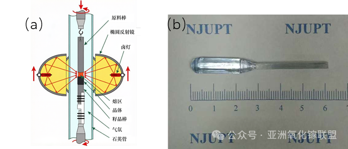
Figure 1(b) shows an unintentionally doped (UID) β-Ga₂O₃ crystal grown using the FZ method.
CZ Method: Mature Cylindrical Crystal Growth Technology
The Czochralski (CZ) method is one of the most mature industrial crystal growth techniques and has been widely applied in material systems such as silicon and sapphire. It also represents an important route for the growth of β-Ga₂O₃ single crystals.
The key feature of the CZ method is that a seed crystal is rotated and slowly pulled from the melt, enabling continuous solidification at the solid–liquid interface and resulting in the formation of large-diameter cylindrical single crystals. For β-Ga₂O₃, the CZ method has already been used to produce single crystals with diameters of 2 inches and above, offering strong scalability, well-defined crystal morphology, high throughput, and relatively flexible dopant control.
In typical β-Ga₂O₃ CZ growth, an RF induction-heated iridium (Ir) crucible is used to melt the Ga₂O₃ raw material. A seed crystal is then slowly dipped into the melt surface and rotated while being pulled upward under a controlled temperature gradient. This enables directional solidification at the solid–liquid interface, ultimately forming a cylindrical single crystal. The schematic of the process is shown in Fig. 2.
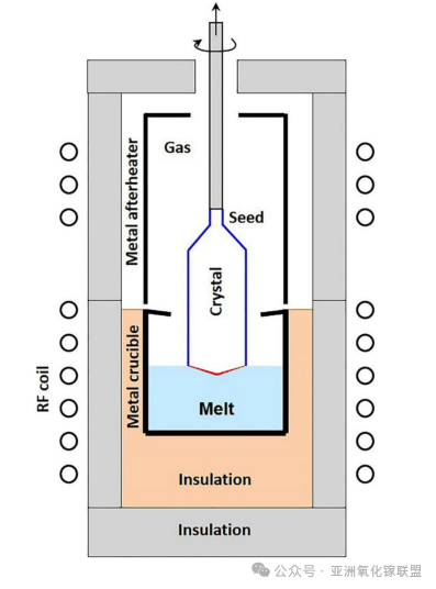
Fig. 2. Schematic illustration of β-Ga₂O₃ crystal growth by the Czochralski (CZ) method [1].
However, the CZ method for growing β-Ga₂O₃ also faces a critical trade-off. On one hand, a certain oxygen partial pressure is required in the growth environment to suppress thermal decomposition of Ga₂O₃ and reduce the volatilization of suboxides. On the other hand, a higher oxygen partial pressure accelerates the oxidation and evaporation of the Ir crucible, leading to increased crucible degradation, shorter lifetime, and higher overall cost. This contradiction becomes particularly pronounced during large-diameter crystal growth and represents one of the key challenges for further industrial-scale development of the CZ method.
At the same time, the CZ method offers significant advantages in dopant engineering. By introducing different dopants into the melt, β-Ga₂O₃ single crystals with tailored electrical properties can be obtained. For example, Mg doping can produce high-resistivity or insulating substrates, while Si doping can yield conductive substrates. Figure 3 illustrates the carrier concentration control in β-Ga₂O₃ single crystals grown by the CZ method. However, at relatively high carrier concentrations, spiral growth patterns appear at the crystal tail, indicating that stable growth of highly conductive β-Ga₂O₃ substrates via the CZ method still faces certain technical limitations.
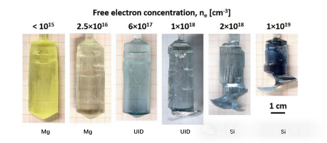
Fig. 3. Carrier concentration control in β-Ga₂O₃ single crystals grown by the CZ method with different doping levels [1].
EFG Method: The Most Commercially Representative Route for Plate-Like Crystals
The Edge-Defined Film-Fed Growth (EFG) method is one of the most representative melt-growth techniques in the commercialization of substrate materials.
Unlike the CZ method, which produces cylindrical crystals, the EFG method enables direct growth of plate-like or specifically shaped single crystals by using a die to define the crystal cross-section. This characteristic is particularly important for substrate applications, as plate-like crystals significantly reduce material loss during subsequent wafer slicing and processing, thereby improving raw material utilization and lowering substrate manufacturing costs.
The growth schematic of β-Ga₂O₃ via the EFG method is shown in Fig. 4. In this process, an RF induction-heated iridium (Ir) crucible is typically used to melt the Ga₂O₃ source material. The melt is then transported upward through a die slit via capillary action, reaching the top of the die. Once a seed crystal contacts the melt at the die top, crystal growth begins as the seed is pulled upward, enabling continuous single-crystal growth.
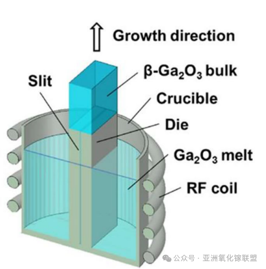
Fig. 4. Schematic illustration of the EFG crystal growth process [2].
Because the crystal cross-section is defined by the die geometry, the resulting crystal maintains a stable plate-like shape. A β-Ga₂O₃ crystal grown by the EFG method is shown in Fig. 5.
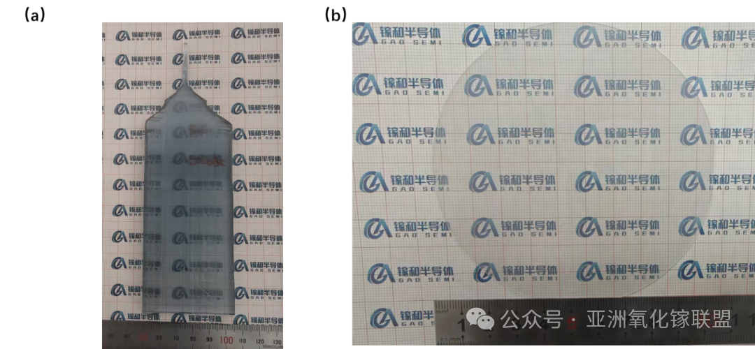
Fig. 5. β-Ga₂O₃ crystal grown by the EFG method.
The EFG method offers clear advantages for large-scale substrate production of β-Ga₂O₃ and has already been used to fabricate large-area single crystals and 6-inch-class substrates. It is currently one of the most commercially mature growth techniques and provides an important source of low-cost, high-throughput homoepitaxial substrates for power device applications.
However, the EFG method is not without challenges. Due to the involvement of die structures, capillary melt transport, solid–liquid interface control, and thermal stress management, issues such as twin formation, bubble inclusion, thickness non-uniformity, and stress-induced cracking may occur. As crystal size continues to scale up, these problems become more pronounced, requiring further optimization in die design, thermal field control, and growth parameter engineering.
VB Method: An Important Route Toward Large-Diameter Cylindrical Crystals
The Vertical Bridgman (VB) method is a classical directional solidification melt-growth technique that has recently attracted increasing attention for the fabrication of large-size β-Ga₂O₃ single crystals.
The basic principle of the VB method is to place Ga₂O₃ raw material inside a crucible and gradually move either the crucible or the heating zone, enabling the melt to solidify directionally from the seed end toward the source end under a controlled temperature gradient. The advancement of the solid–liquid interface is primarily governed by the crucible pulling (or translation) rate and the imposed thermal gradient. The schematic of the growth process and the corresponding temperature gradient distribution are shown in Fig. 6.
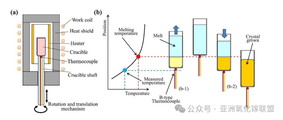
Fig. 6. (a) Schematic illustration of VB crystal growth; (b) temperature gradient distribution in the VB method [4].
Compared with the CZ and EFG methods, the VB process is closer to a bulk directional solidification approach. This makes it particularly suitable for growing large-diameter bulk crystals and provides strong potential for further diameter scaling. At present, the VB method has already been used to fabricate 6-inch-class β-Ga₂O₃ single crystals, as shown in Fig. 7, making it one of the key technological routes toward industrial-scale large-area substrates.
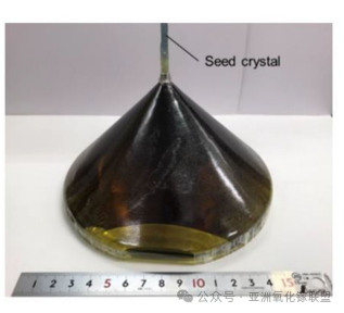
Fig. 7. 6-inch β-Ga₂O₃ single crystal grown by the VB method [3].
A key advantage of the VB method lies in its choice of crucible materials. Both CZ and EFG techniques typically rely on iridium (Ir) crucibles, which are prone to oxidation and volatilization in high-temperature oxygen-containing environments, leading to increased crucible degradation and cost. In contrast, the VB method can utilize Pt/Rh alloy crucibles, which exhibit better structural stability and oxidation resistance near 1800°C, thereby helping to mitigate crucible loss issues during growth.
Therefore, the VB method not only offers strong potential for scaling to large crystal sizes, but also provides advantages in reducing crucible consumption, improving growth stability, and enabling more cost-effective production of β-Ga₂O₃ substrates.
However, the VB method also faces several process challenges. During large-diameter crystal growth, precise control of the temperature gradient, solid–liquid interface shape, and cooling process is required; otherwise, thermal stress, cracking, dislocation formation, and compositional or doping inhomogeneities may occur. For β-Ga₂O₃, which exhibits low symmetry, strong anisotropy, and pronounced cleavage planes, thermal-field design and stress management are particularly critical.
Casting Method: A Fast-Scaling Route Toward Larger-Size Crystals
Although traditional melt-growth methods such as CZ, EFG, and VB have already enabled the development of β-Ga₂O₃ substrates from small sizes up to the 2–6 inch range, they still face several limitations, including long high-temperature growth cycles, high costs associated with precious-metal crucibles, and difficulties in further scaling crystal size.
To address these challenges and achieve lower cost, larger dimensions, and higher growth efficiency, the Casting method has recently attracted growing attention.
The Casting method is an emerging melt-growth approach aimed at the fabrication of large-volume crystals. Unlike conventional single-crystal pulling techniques, it emphasizes a high-throughput, bulk directional solidification process. The core idea is to fully melt the raw material and then solidify it under controlled conditions, enabling the formation of large-area crystals.
Compared with traditional melt-growth techniques, the Casting method demonstrates strong potential for size scaling, with successful exploratory demonstrations ranging from 2-inch to 8-inch β-Ga₂O₃ crystals. Figure 8 shows an 8-inch β-Ga₂O₃ crystal grown using the Casting method.
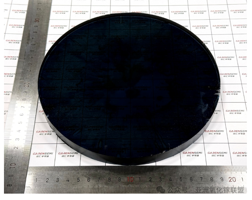
Fig. 8. 8-inch β-Ga₂O₃ crystal grown by the Casting method [5].
However, the Casting method is still in a developmental and optimization stage. Due to the complexity of thermal-field evolution, interface morphology, and stress relaxation during bulk solidification, key challenges remain in maintaining crystal orientation uniformity, reducing defect density, suppressing cracking, and improving machinability. These issues must be addressed before the technique can be fully transitioned into industrial-scale production.
OCC Method: A New Approach Beyond Precious-Metal Crucibles
In addition to the Casting method, the Optical Cold Crucible (OCC) method has emerged in recent years as another promising route for β-Ga₂O₃ single-crystal growth.
The most distinctive feature of the OCC method compared with conventional melt-growth techniques is that it eliminates the need for precious-metal crucibles such as iridium (Ir) or platinum (Pt). Instead, it utilizes a “self-supporting crucible” formed by solid β-Ga₂O₃ itself, thereby preventing direct contact between the melt and metal containers.
In the OCC process, a water-cooled copper structure is typically placed around the growth zone. Since Ga₂O₃ has relatively low electrical conductivity at room temperature, the initial heating stage often requires auxiliary absorbers or initiators, such as metallic Ga, Ir rings, or carbon sheets, to assist in electromagnetic energy absorption and provide initial heating.
As the temperature increases, the electrical conductivity of Ga₂O₃ significantly improves, allowing the melt to couple directly with the high-frequency electromagnetic field for induction heating. At the same time, the water-cooled copper walls rapidly solidify the melt near the boundary region, forming a dense solid outer shell. This shell effectively acts as a “self-formed crucible,” partially replacing conventional precious-metal containers.
The advantages of the OCC method are clear: it significantly reduces reliance on expensive Ir or Pt crucibles, thereby lowering material costs and mitigating crucible-related contamination. As shown in Fig. 9, β-Ga₂O₃ single crystals grown by the OCC method have already reached diameters of approximately 45 mm.
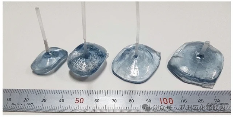
Fig. 9. β-Ga₂O₃ single crystal grown by the OCC method [6].
However, at its current stage of development, the OCC method is still far from industrial-scale production of large-area substrates. Key challenges include melt stability control, thermal-field uniformity, crystal size scaling, improvement of crystal quality, and process repeatability. Nevertheless, the OCC approach—based on the concept of “crucible-free growth without precious metals”—offers a valuable new direction for low-cost β-Ga₂O₃ crystal growth.
Summary of This Issue
The ability of β-Ga₂O₃ to achieve large-size substrate production stems not only from its excellent intrinsic properties, such as an ultra-wide bandgap and high breakdown field, but more importantly from its compatibility with melt-growth techniques.
Compared with GaN, SiC, and diamond, the high-temperature melt of β-Ga₂O₃ is not fully stable; however, its decomposition and volatilization can be effectively suppressed by controlling oxygen partial pressure. This enables single-crystal growth and size scaling within a relatively mature process window.
From the perspective of growth technologies, the FZ method is suitable for high-purity small crystals and fundamental research; CZ, EFG, and VB methods form the core framework for large-size substrate production; while emerging approaches such as Casting and OCC point toward future directions of lower cost, higher throughput, and even larger crystal dimensions.
Therefore, the industrial potential of β-Ga₂O₃ does not lie only in its superior material properties, but also in its manufacturability. Melt growth provides a critical pathway toward scalable, low-cost substrate supply, which is a key advantage distinguishing β-Ga₂O₃ from many other ultra-wide bandgap semiconductors. With continuous advances in growth techniques, thermal-field engineering, crucible materials, and defect control, β-Ga₂O₃ substrates are expected to further evolve toward larger sizes, higher quality, and lower cost, laying a solid materials foundation for future power electronic applications.
Referance:
[1] Z. Galazka, J. Appl. Phys. 131(3), 031103 (2022)
[2] A. Kuramata, K. Koshi, S. Watanabe et al., Jpn. J. Appl. Phys. 55(12), 1202A1202 (2016)
[3] https://www.novelcrystal.co.jp/eng/2023/2340/, (2023).
[4] K. Hoshikawa, E. Ohba, T. Kobayashi et al., J. Cryst. Growth 447, 36–41 (2016)
[5] http://www.garen.cc/newsx.php?lm=14&id=72 (2025)
[6] A. Yoshikawa, V. Kochurikhin, T. Tomida et al., Sci. Rep. 14(1), 14881 (2024)
