Paper Sharing
【International Papers】Effects of nitrogen radical irradiation on device characteristics of vertical β-Ga₂O₃(010) FinFETs
日期:2026-06-16阅读:50
Researchers from National Institute of Information and Communications Technology, Osaka Metropolitan University, Tokyo University of Agriculture and Technology, Nippon Sanso Corporation have published a dissertation titled " Effects of nitrogen radical irradiation on device characteristics of vertical β-Ga₂O₃(010) FinFETs " in APL Electronic Devices.
Background
β-Ga₂O₃ is an ultra-wide bandgap semiconductor with a bandgap of 4.5 eV and an ultrahigh critical electric field of 7 MV/cm, which is widely studied for high-power electronic devices. Donor doping technologies using Si and Sn have been well developed for β-Ga₂O₃, while the material is limited to unipolar devices due to the lack of shallow acceptors and self-trapped holes. Deep acceptor doping with N and Mg is commonly used to form current blocking layers. Low thermal conductivity makes lateral devices prone to thermal failure, and vertical FinFETs possess superior gate control performance. Reactive ion etching will generate dangling bonds and charged impurities on device sidewalls, degrading device performance and causing threshold voltage fluctuation. Conventional wet etching cannot fully remove etching defects, so novel surface treatment methods are urgently needed.
Abstract
We investigated effects of nitrogen radical irradiation on device characteristics of vertical β-Ga₂O₃ (010) finfield-effect transistors (FinFETs). A positive shift in threshold voltage with improved in-plane distribution uniformity occurred for nitridated FinFETs due to fixed negative charges formed in nitridated layers on fin sidewalls, indicating that the nitridation treatment can effectively re-establish the post-etched sidewall surface conditions. The breakdown voltage (Vbr) was also uniformly distributed for the nitridated FinFETs, while the specific onresistance (Ron) was reduced by adopting multi-fin structure and increasing fin width. The nitridated Ga₂O₃ (010) multi-FinFET with a fin width of 300 nm achieved normally off operation with superior device characteristics of a subthreshold swing of 73 mV/decade, an Ion/Ioff ratio of >10¹⁰, an Ron of 9.5 mΩ cm², a Vbr of 1213 V, and a power figure of merit of 1.55 ×10⁸ W/cm².
Highlights
Nitrogen radical irradiation is adopted to repair plasma etching damage on β-Ga₂O₃ FinFET sidewalls.
Nitridation treatment realizes positive shift of threshold voltage and greatly improves the uniformity of device parameters.
Optimizing multi-fin structure and fin width effectively reduces the specific on-resistance of devices.
The fabricated device exhibits excellent comprehensive performance including high breakdown voltage and outstanding power figure of merit.
Conclusion
In summary, we investigated effects of N radical irradiation on device characteristics of Ga₂O₃ (010) FinFETs. At Wfin=200 nm, the Vth shift from 0.65±0.25 V for the non-nitridated FinFETs to 1.35±0.15 V for the nitridated ones was observed, which can be attributed to formation of negative fixed charges in the nitridated layer on the fin sidewall surface. Furthermore, an improvement in in-plane uniformity of Vth was obtained for the nitridated FinFETs, indicating that the nitridation is effective in re-establishing the surface condition after plasma etching. The nitridated multi-FinFET with Wfin=300 nm achieved an enhancement-mode operation with a SS of 73 mV/decade, an Ion/Ioff ratio of >1010, an Ron of 9.5 mΩ cm2, a Vbr of 1213 V, and a power figure of merit of 1.55×10⁸ W/cm2. These results indicate that N radical irradiation can be a useful technique to fabricate normally off Ga₂O₃ FinFETs with an excellent in-plane uniformity of device performance.
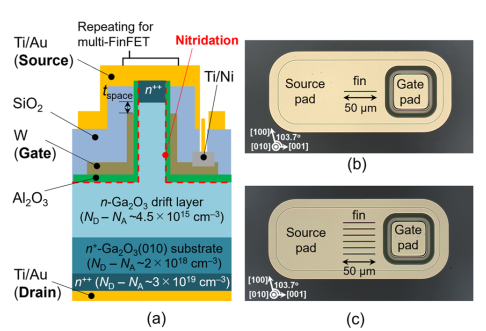
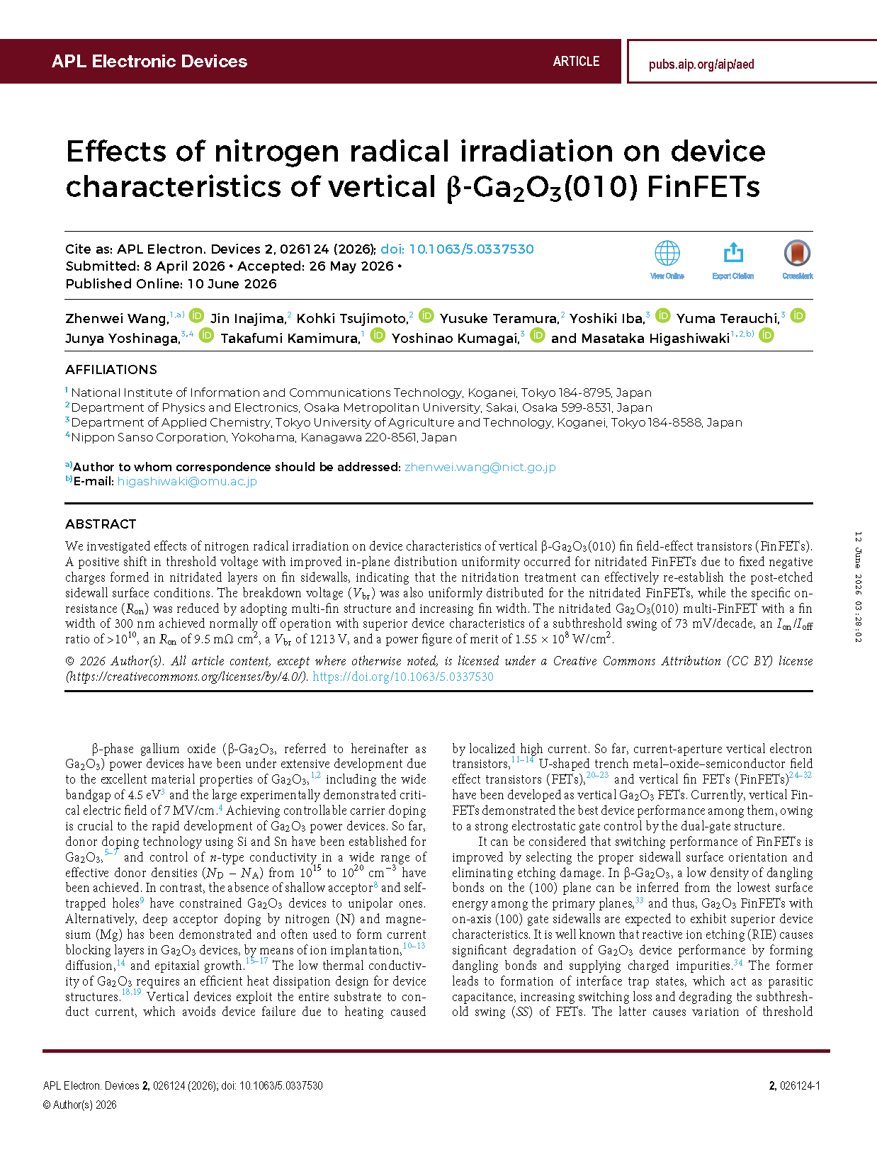
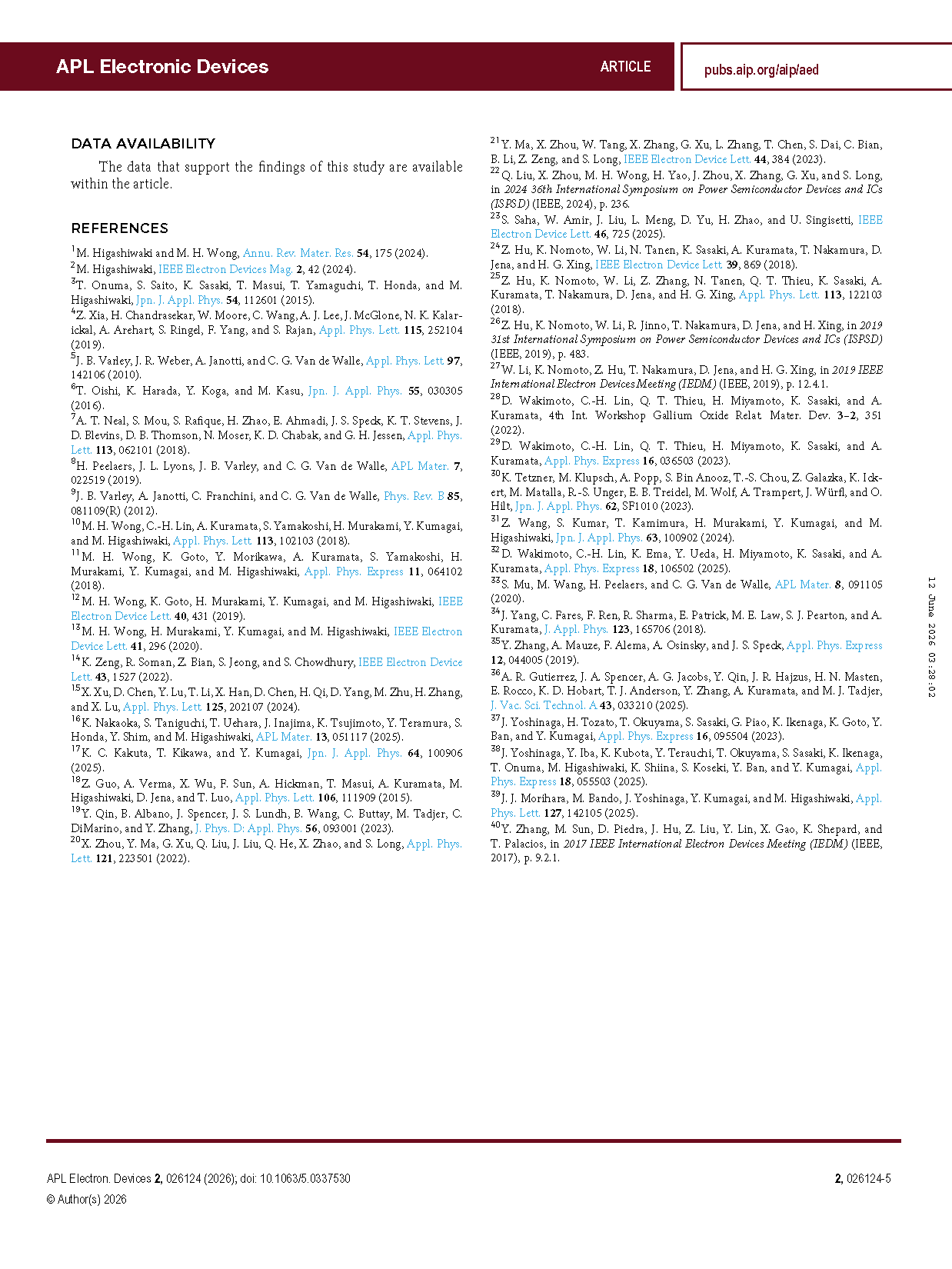
FIG. 1. (a) Cross-sectional schematic of vertical FinFET structure on n⁺-Ga₂O₃ (010) substrate. The nitridated interface is indicated by the red dashed line. Plane-view micrographs of (b) single- and (c) multi-FinFETs.
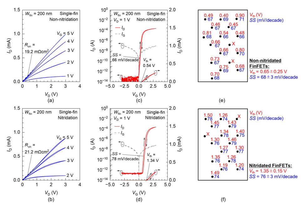
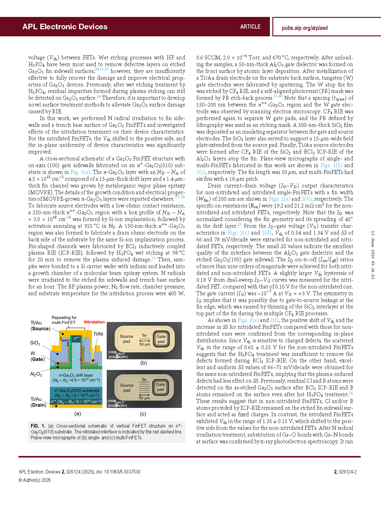
FIG. 2. ID–VD output characteristics of (a) non-nitridated and (b) nitridated single-FinFETs. ID–VG transfer characteristics of (c) non-nitridated and (d) nitridated single-FinFETs. Mappings of Vth and SS for (e) non-nitridated and (f) nitridated single-FinFETs fabricated on substrates with a size of 15 × 10 mm². In panels (e) and (f), actual device positions are specified by dots; the "x" mark indicates a device that shows no FET operation, due to device processing issues.
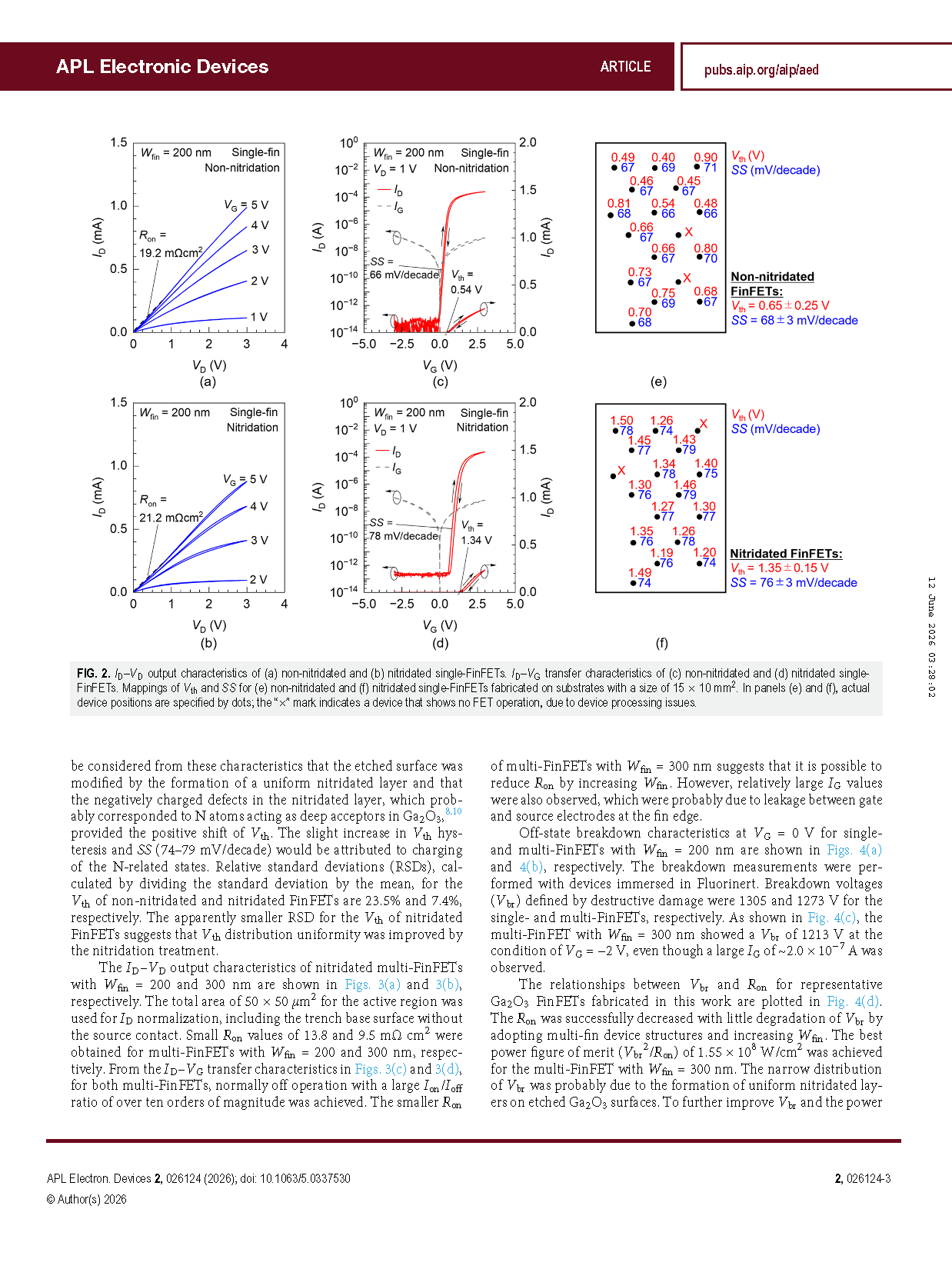
FIG. 3. ID–VD output and ID–VG transfer characteristics for multi-FinFETs with (a) and (c) Wfin = 200 and (b) and (d) 300 nm, respectively.
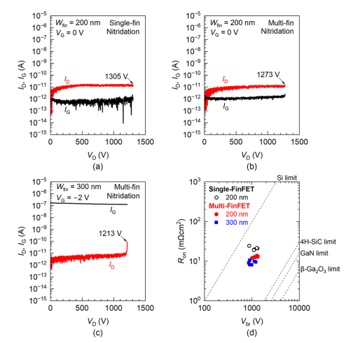
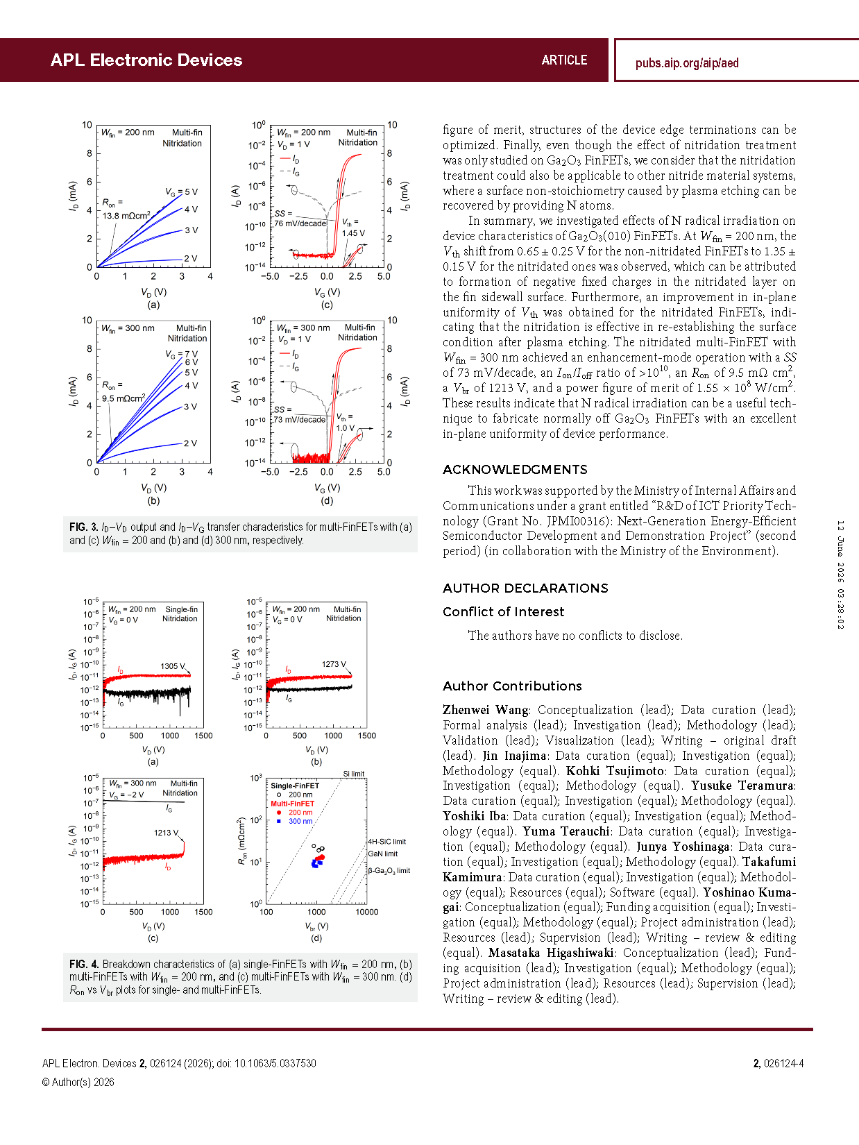
FIG. 4. Breakdown characteristics of (a) single-FinFETs with Wfin = 200 nm, (b) multi-FinFETs with Wfin = 200 nm, and (c) multi-FinFETs with Wfin = 300 nm. (d) Ron vs Vbr plots for single- and multi-FinFETs.
DOI:
doi.org/10.1063/5.033753