Paper Sharing
【Member Papers】Recent Advances in Vertical β-Ga₂O₃ Power Devices: Epitaxy, Processing, and Performance
日期:2026-06-16阅读:56
Researchers from the ShanghaiTech University and Donghua University have published a dissertation titled " Recent Advances in Vertical β-Ga2O3 Power Devices: Epitaxy, Processing, and Performance " in Semiconductor Science and Technology.
Background
The performance of traditional silicon-based power devices can no longer meet the requirements of power electronic systems for high power density and high operating frequency. As a new generation of ultra-wide bandgap semiconductor, β-Ga₂O₃ has a bandgap of about 4.9 eV and a theoretical critical breakdown electric field up to 8 MV/cm. Large-size and low-cost single-crystal substrates can be fabricated by melt growth method. It is superior to silicon, silicon carbide and gallium nitride, and becomes an ideal candidate for high-voltage and high-efficiency power devices.
Compared with lateral devices, vertical β-Ga₂O₃ power devices have uniform electric field distribution, large current carrying capacity, high area utilization and excellent heat dissipation, which have become the mainstream research direction. At present, there are still many technical challenges: epitaxial layers contain abundant defects and lead to poor device stability; it is difficult to realize efficient and stable p-type doping for β-Ga₂O₃, so high-quality homogeneous p-n junctions cannot be fabricated; the intrinsic thermal conductivity of the material is low, which easily causes thermal failure under high-power operation. In addition, the edge termination technology and device reliability under radiation and extreme temperature also need further optimization.
This paper comprehensively reviews the research progress of vertical β-Ga₂O₃ power devices. It compares the characteristics and application scenarios of three mainstream epitaxial technologies including HVPE, MOCVD and MBE. The structure, fabrication process and performance of Schottky barrier diodes, p-n heterojunction diodes and vertical transistors are analyzed. Staged solutions for p-type doping and thermal management are proposed. This work provides references for the follow-up research and industrialization of β-Ga₂O₃ power devices.
Abstract
The growing demand for higher power density and operational frequency in power conversion systems is driving the development of devices that exceed the limits of conventional silicon. Beta-phase gallium oxide (β-Ga₂O₃) has emerged as a highly promising ultra-wide-bandgap semiconductor for next-generation high-voltage and high-efficiency power electronics. This promise stems from its exceptional material properties, including a large bandgap (~4.9 eV), a high theoretical critical electric field (8 MV/cm), and the availability of large-area, low-cost melt-grown substrates. These intrinsic characteristics facilitate vertical device architectures that can achieve unprecedented breakdown voltages while minimizing conduction losses. However, several key challenges currently limiting the application of vertical β-Ga₂O₃ devices must be addressed, including epitaxial quality, device degradation, low p-type doping efficiency, and inadequate thermal management. Overall, this review highlights the significant potential of vertical β-Ga₂O₃ power devices, which is being realized through rapid advancements in epitaxial growth, device fabrication, and defect control. Furthermore, achieving the full potential of β-Ga₂O₃ in high-power applications will require continued advances in p-type conductivity and thermal dissipation. The methodologies outlined may have broader applicability to other emerging semiconductor materials.
Highlights
A systematic comparison of HVPE, MOCVD and MBE epitaxial technologies for β-Ga₂O₃, including growth rate, crystal quality, production capacity and existing defects.
Comprehensive summary of structural design, edge termination techniques and electrical parameters of vertical Schottky diodes, p-n heterojunction diodes and various vertical transistors.
In-depth analysis of device degradation mechanisms under thermal, electrical and radiation stress, and the influence of killer defects on device performance.
Propose three-stage technical routes for p-type doping of β-Ga₂O₃, and establish thermal management strategies at device and package levels.
Prospect the commercialization route and future research priorities of vertical β-Ga₂O₃ power devices.
Conclusion
This review has discussed critical aspects of β-Ga₂O₃ technology for power electronics, encompassing epitaxial growth, vertical device architectures, and potential optimization strategies for p-type doping and thermal management. β-Ga₂O₃ devices are positioned to play a significant role in next-generation power converters. Prior to its large-scale commercialization, the following critical challenges must be addressed.
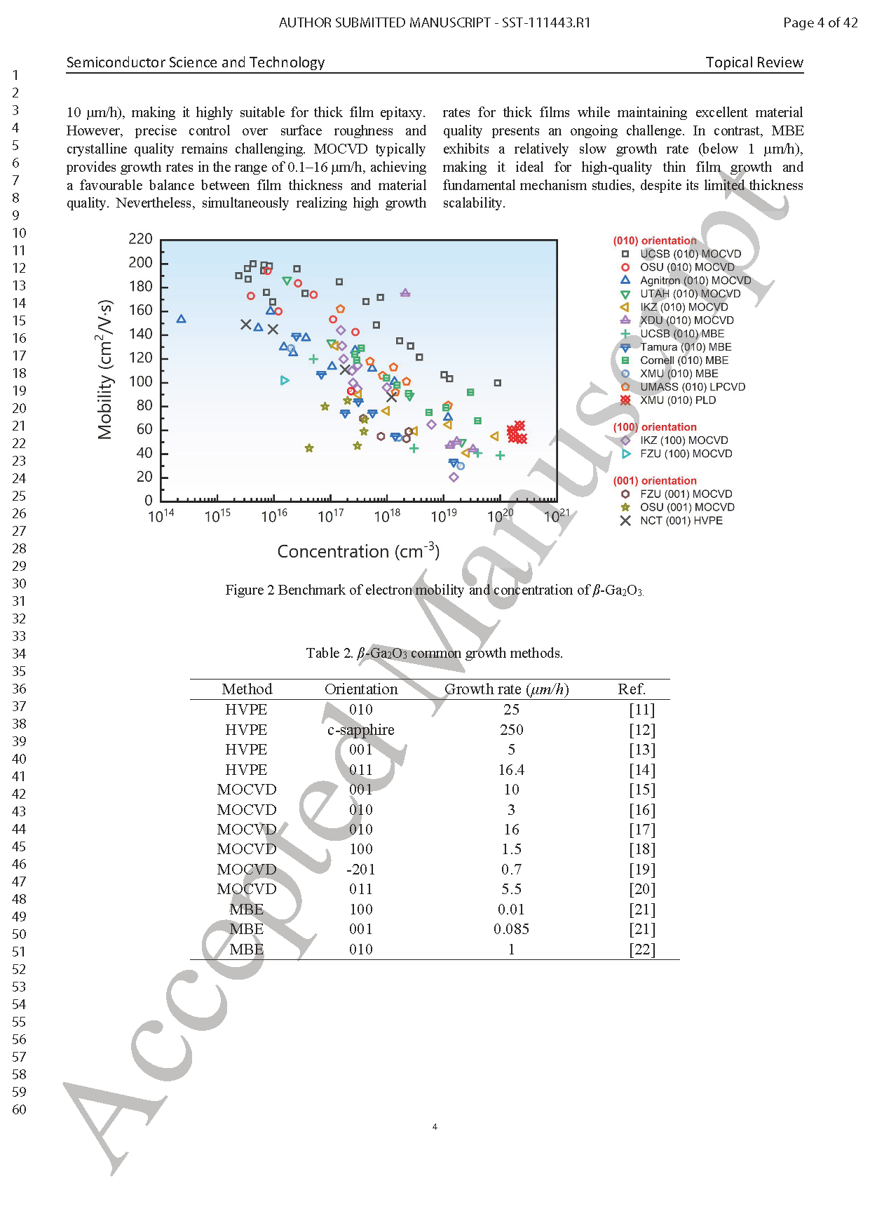
Epitaxial growth techniques like HVPE, MOCVD, and MBE have advanced vertical device architectures, laying the groundwork for high-performance β-Ga₂O₃ power electronics. Among them, HVPE excels in mass production with low cost, MOCVD enables precise control with favourable growth rate, and MBE facilitates high-quality film fabrication. To promote their practical applications, β-Ga₂O₃ epitaxy still needs to continuously reduce defect density and ensure uniformity, especially on large-size substrates.
Vertical devices have shown rapid performance advances, with BV over 10 kV demonstrated. However, their performance remains far below the intrinsic material limits, mainly due to the material defects, immature processes and unclear reliability mechanisms. One of key priorities is identifying and suppressing killer defects that degrade breakdown characteristics. Meanwhile, improving interface quality and relieving electric field crowding via efficient edge terminations are also critical to boost blocking voltages. Additionally, a low-resistance Au-free ohmic contacts is essential to reduce conduction losses.
Alongside advancements in β-Ga₂O₃ material and device technology, addressing p-type doping and thermal management remains a pivotal challenge. Unreliable p-type doping restricts CMOS compatibility, and causes device reliability issues. Device and package-level thermal management will be essential for the suppression of self-heating. Developing integrated structures and exploring heterostructures can further boost device performance.
Through interdisciplinary collaboration, β-Ga₂O₃ vertical devices could transform power electronics and meet global energy demands. As their performance matures, they are expected to engage in increasingly robust competition with established Si and SiC technologies in the coming years.
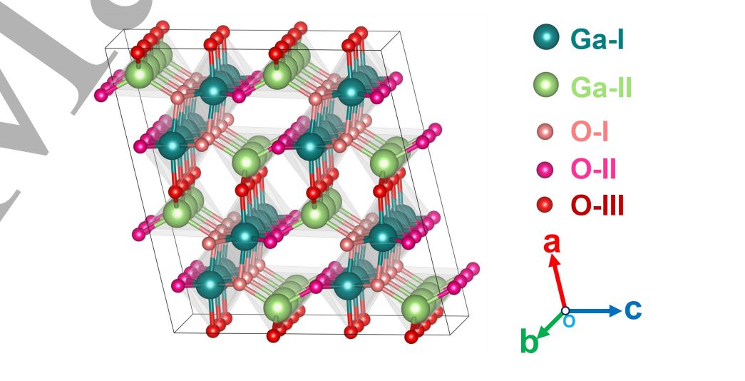
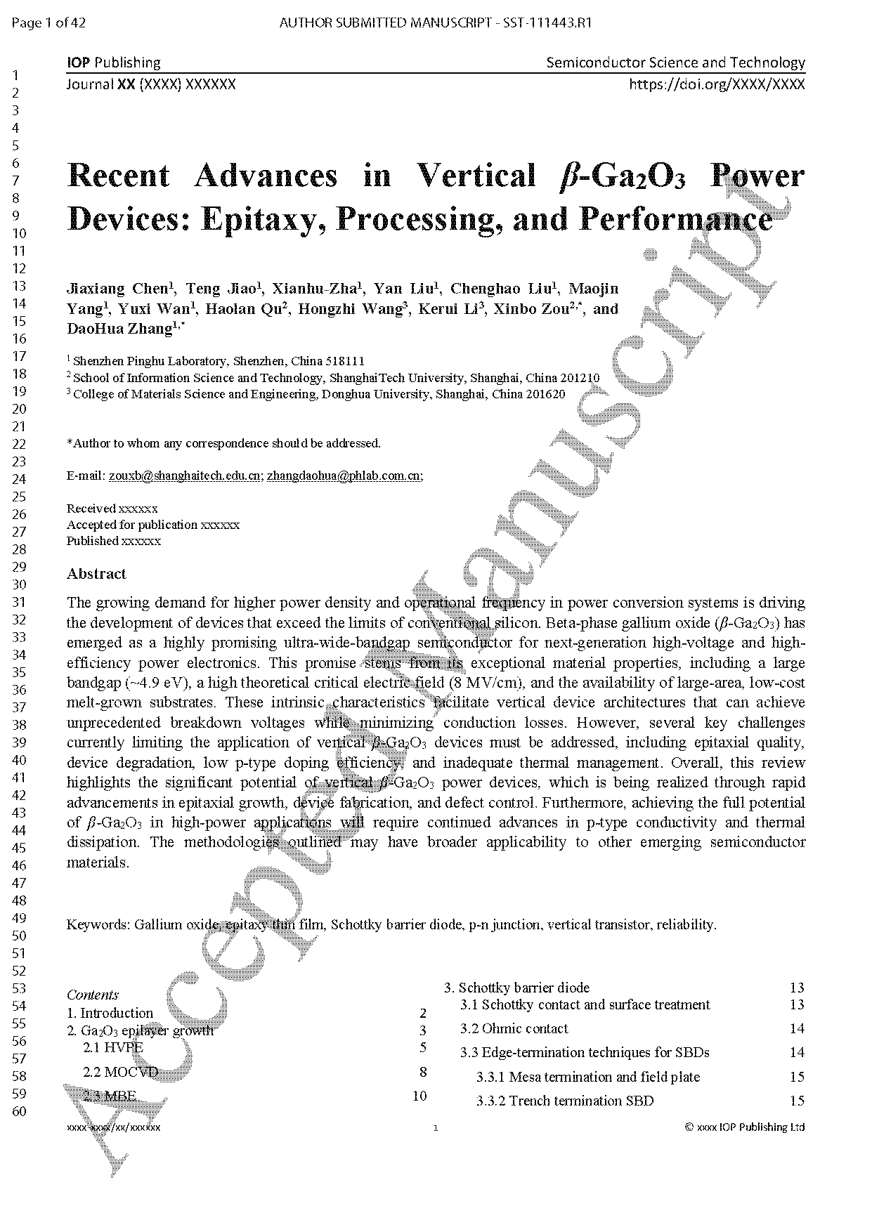
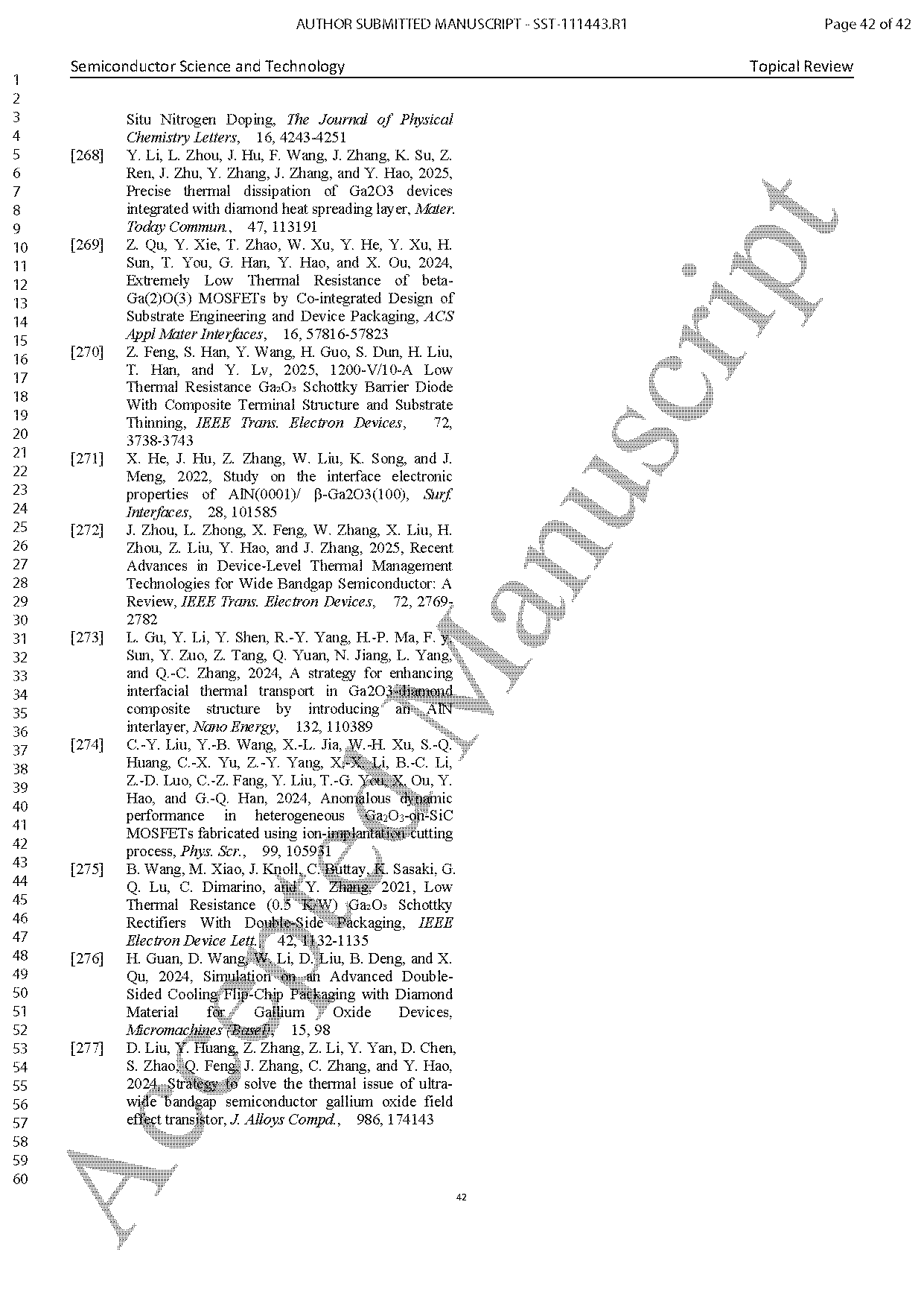
Fig. 1. β-Ga₂O₃ crystal supercell structure based on its conventional unit cell.
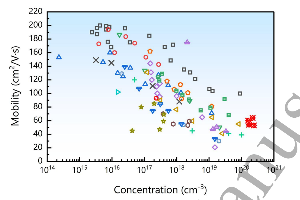
Fig. 2. Benchmark of electron mobility and concentration of β-Ga₂O₃.
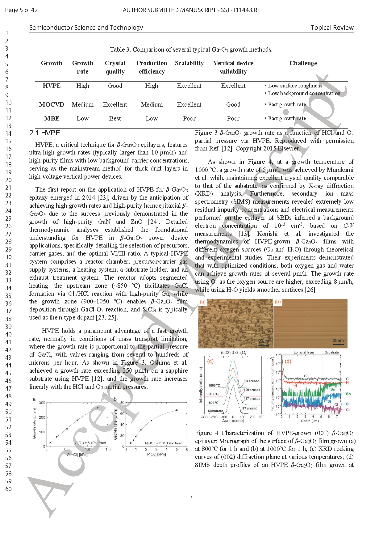
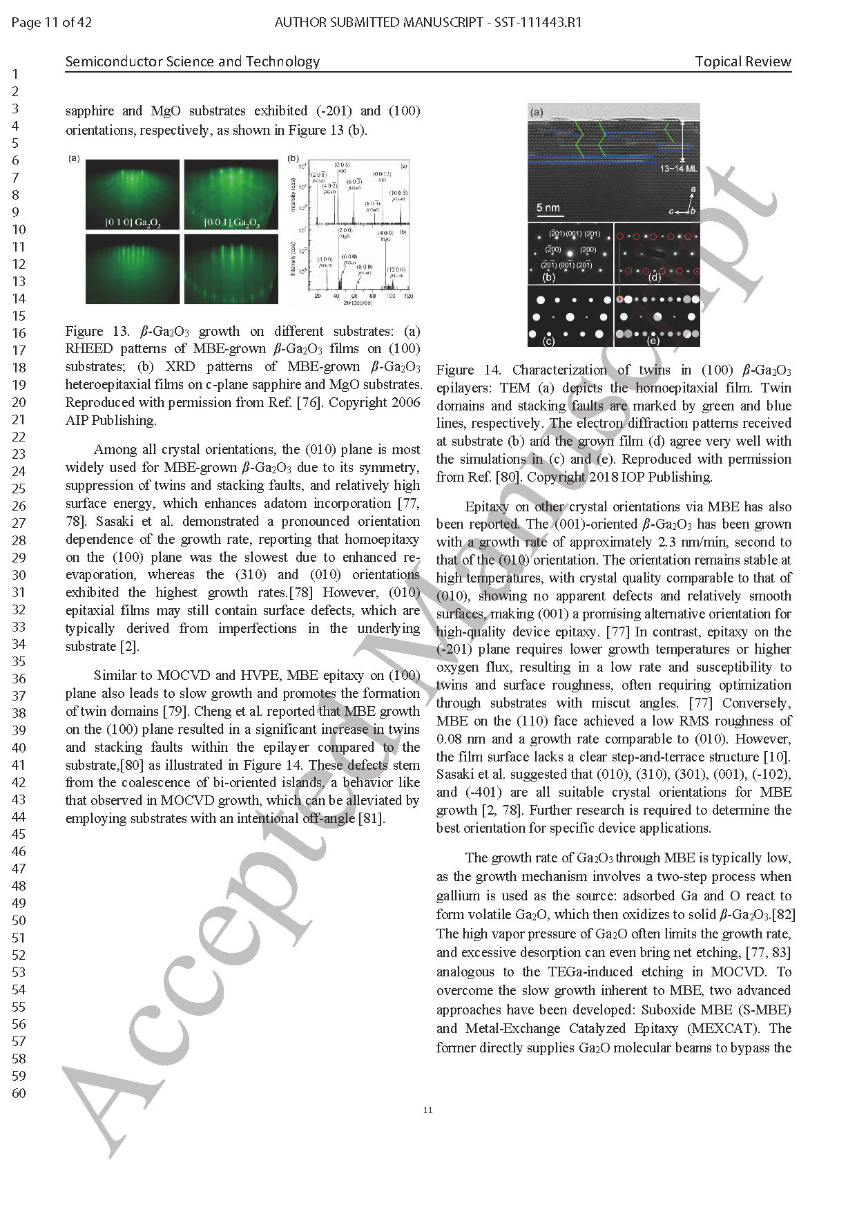
Fig. 3. Characterization of HVPE-grown (001) β-Ga₂O₃ epilayer: Micrograph of the surface of β-Ga₂O₃ film grown (a) at 800℃ for 1 h and (b) at 1000℃ for 1 h; (c) XRD rocking curves of (002) diffraction plane at various temperatures; (d) SIMS depth profiles of an HVPE β-Ga₂O₃ film grown at 1000°C.
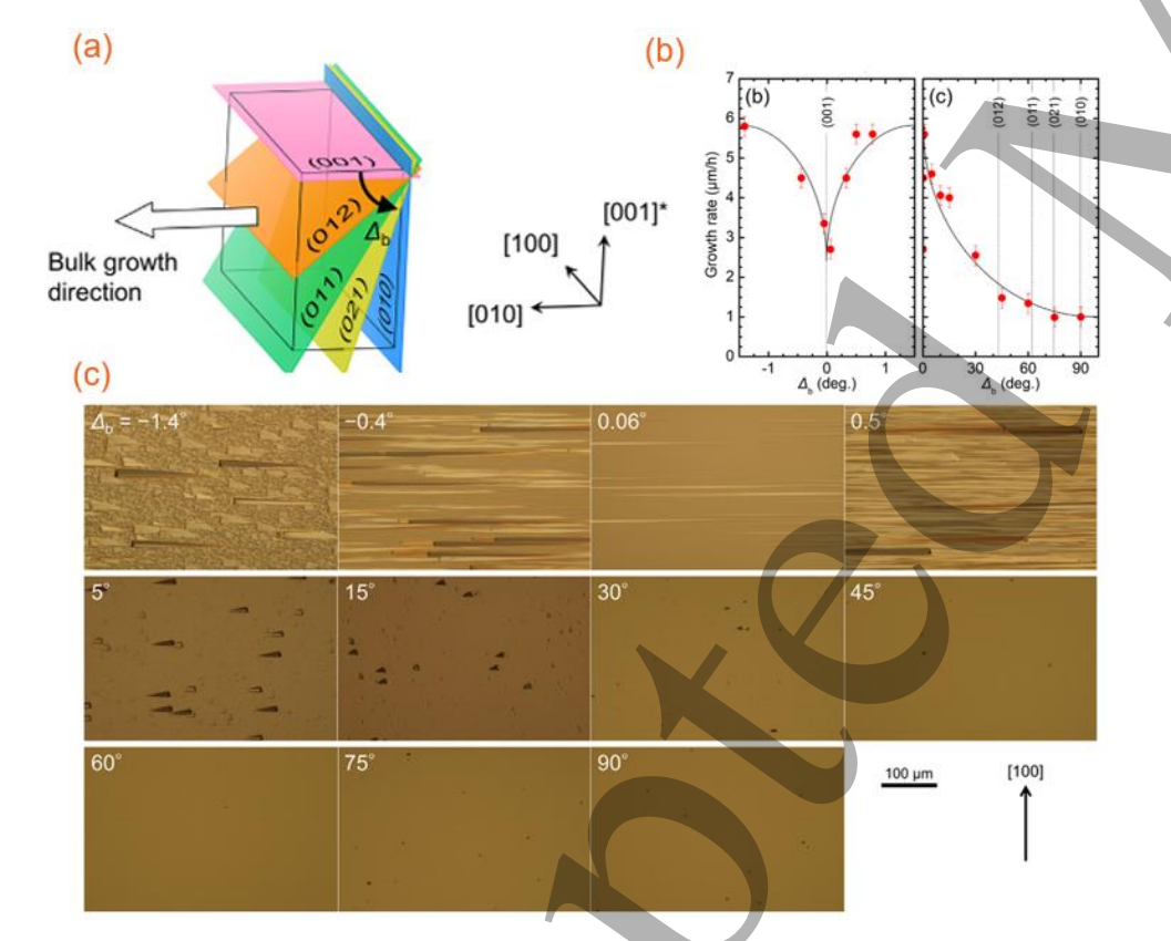
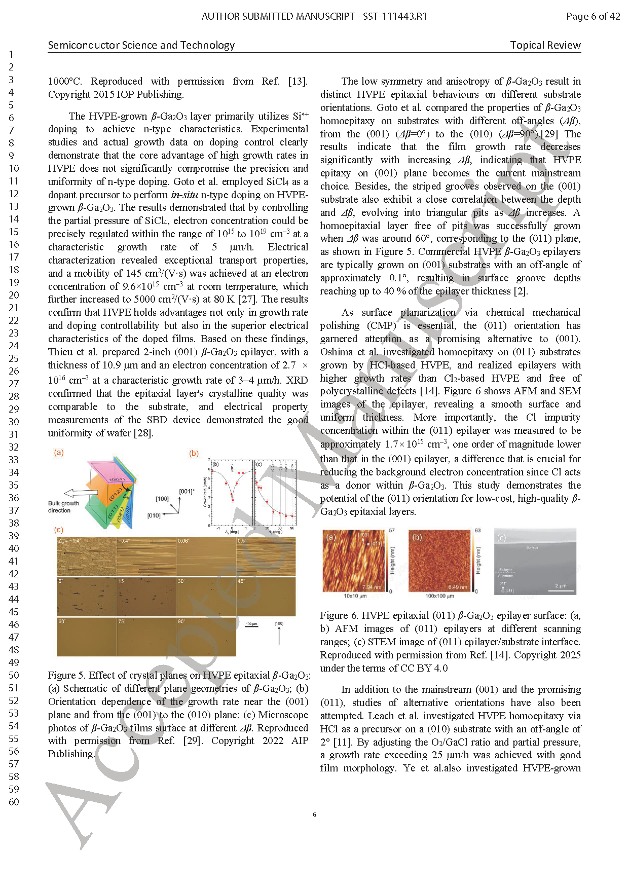
Fig. 4. Effect of crystal planes on HVPE epitaxial β-Ga₂O₃: (a) Schematic of different plane geometries of β-Ga₂O₃ (b) Orientation dependence of the growth rate near the (001) plane and from the (001) to the (010) plane; (c) Microscope photos of β-Ga₂O₃ films surface at different Δβ.
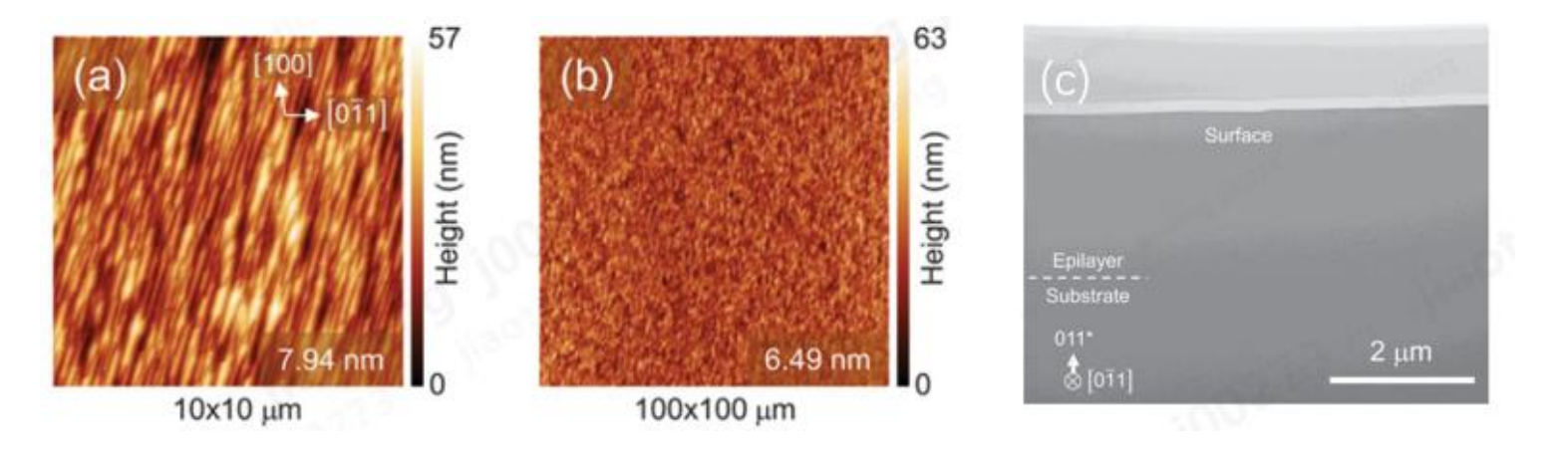
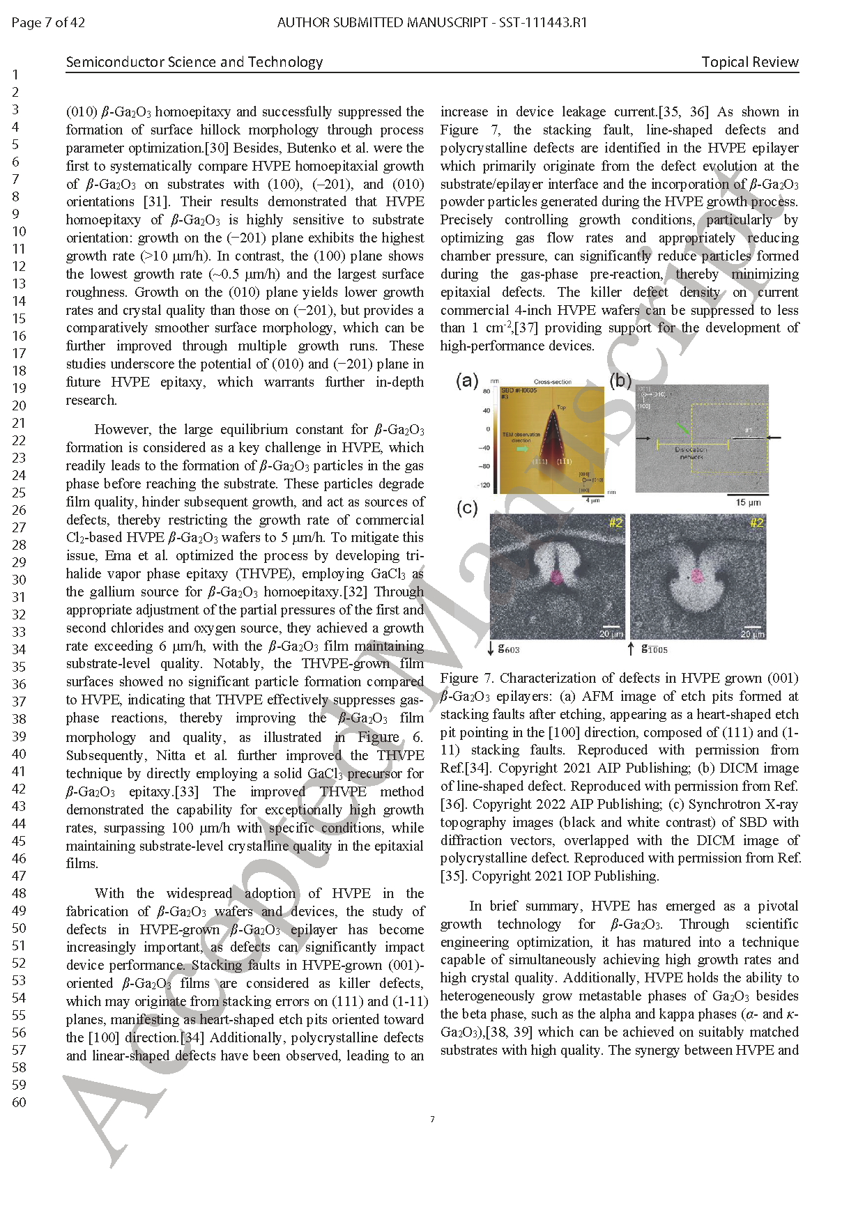
Fig. 5. HVPE epitaxial (011) β-Ga₂O₃ epilayer surface: (a, b) AFM images of (011) epilayers at different scanning ranges; (c) STEM image of (011) epilayer/substrate interface.
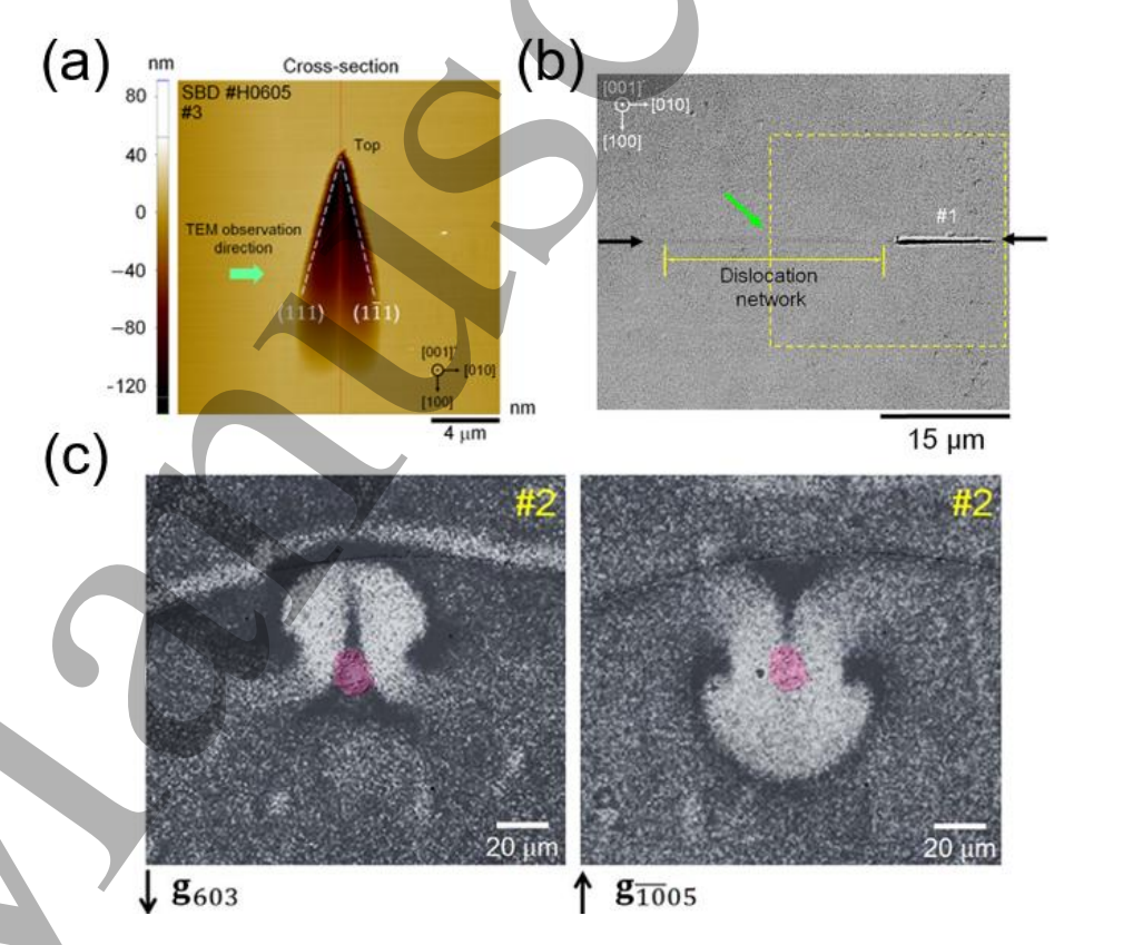
Fig. 6. Characterization of defects in HVPE grown (001) β-Ga₂O₃ epilayers: (a) AFM image of etch pits formed at stacking faults after etching, appearing as a heart-shaped etch pit pointing in the [100] direction, composed of (111) and (1-11) stacking faults. (b) DICM image of line-shaped defect. (c) Synchrotron X-ray topography images (black and white contrast) of SBD with diffraction vectors, overlapped with the DICM image of polycrystalline defect.
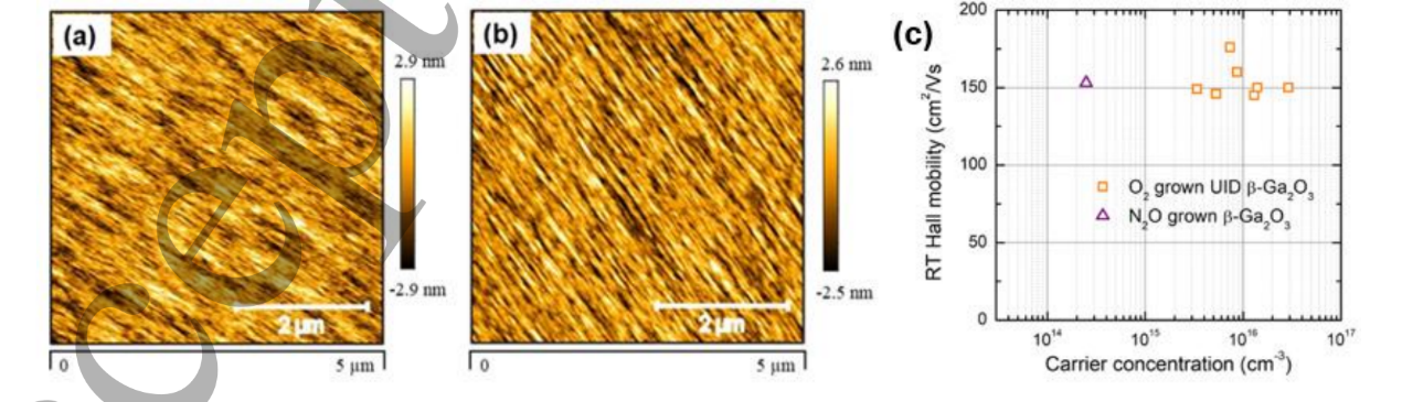
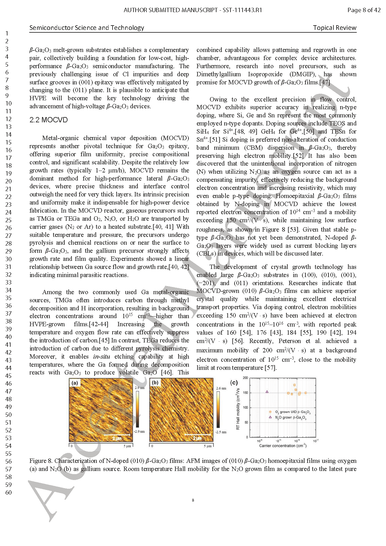
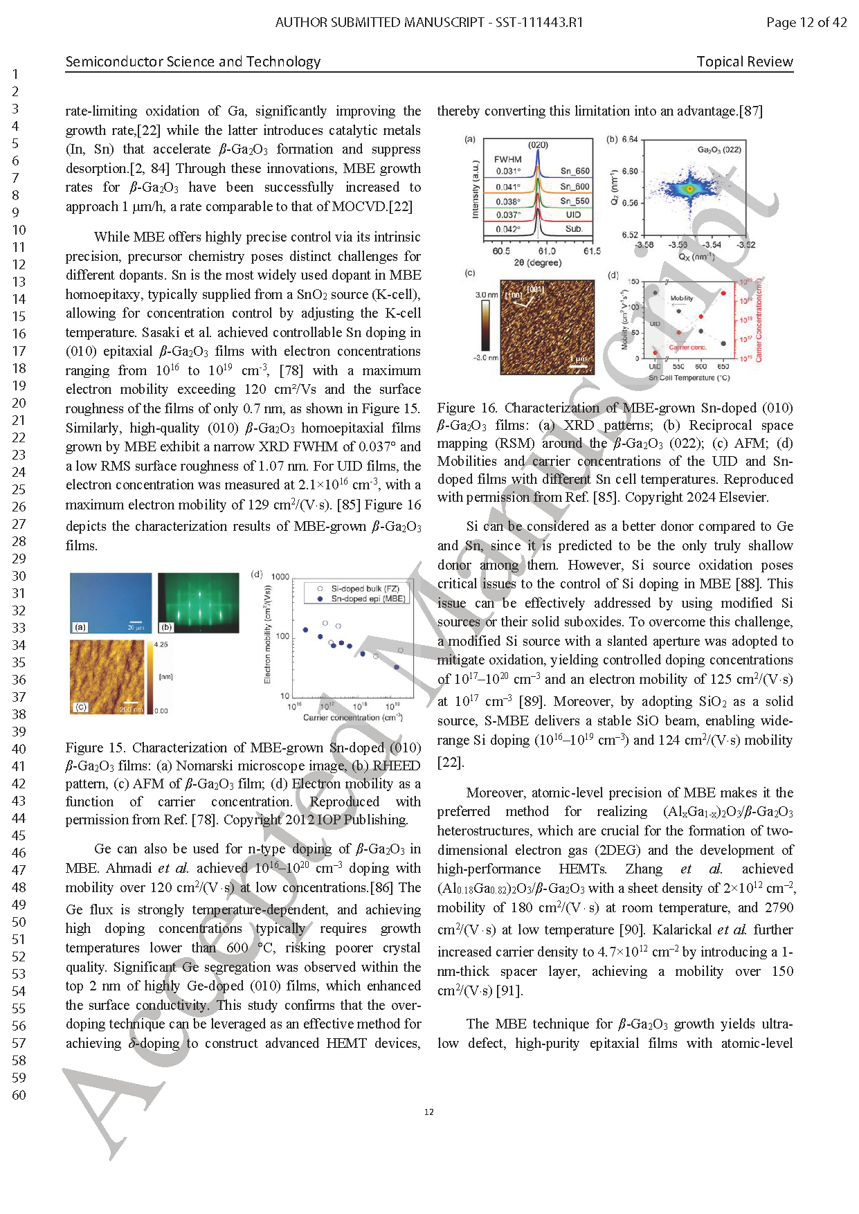
Fig. 7. Characterization of N-doped (010) β-Ga₂O₃ films: AFM images of (010) β-Ga₂O₃ homoepitaxial films using oxygen (a) and N₂O (b) as gallium source. (c) Room temperature Hall mobility for the N₂O grown film as compared to the latest pure β-Ga₂O₃.
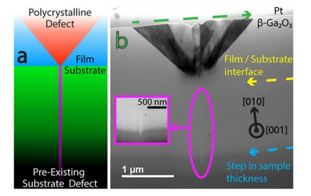
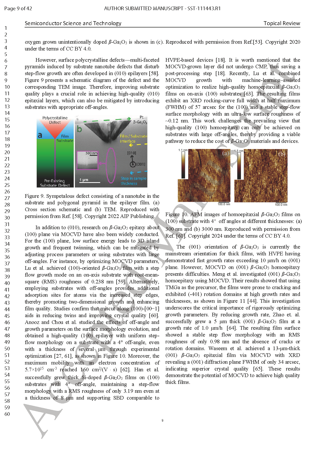
Fig. 8. Sympetalous defect consisting of a nanotube in the substrate and polygonal pyramid in the epilayer film. (a) Cross section schematic and (b) TEM.
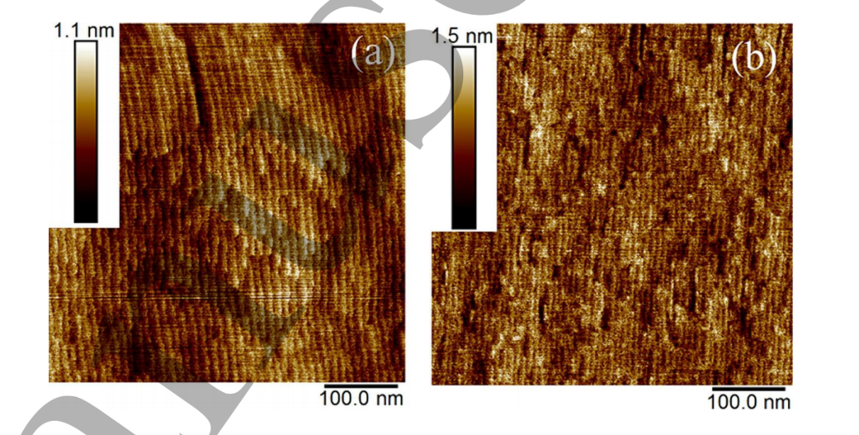
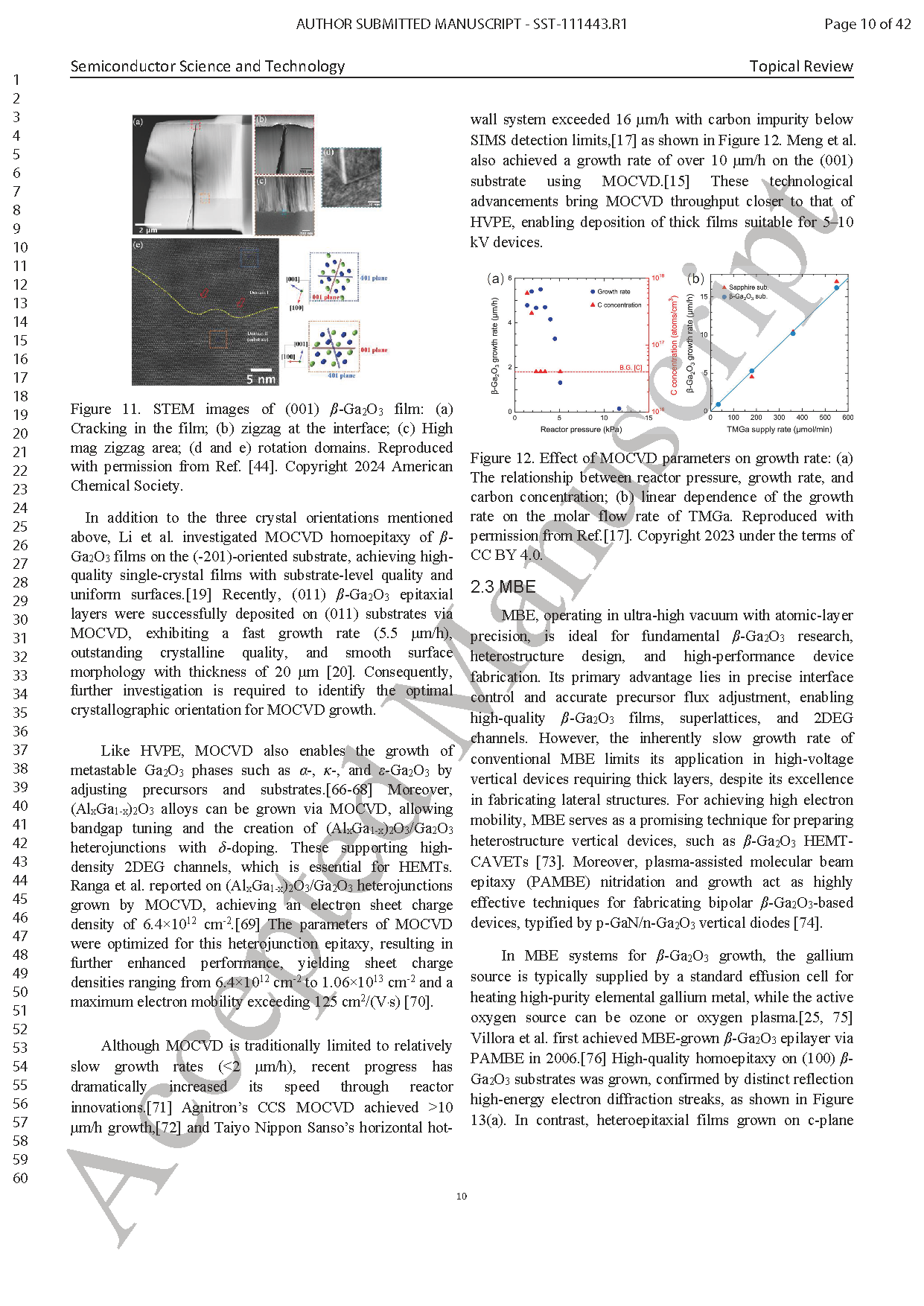
Fig. 9. AFM images of homoepitaxial β-Ga₂O₃ films on (100) substrate with 4° off angles at different thicknesses: (a) 300 nm and (b) 3000 nm
DOI:
10.1088/1361-6641/ae7ab3