Paper Sharing
【Domestic Papers】Single-Event Effects and Corresponding Nanoscale Microstructure in β-Ga₂O₃ UMOSFETs: Device Reliability and Failure Mechanism
日期:2026-06-17阅读:47
Researchers from the University of Science and Technology of China and Harbin Institute of Technology and Chinese Academy of Sciences have published a dissertation titled " Single-Event Effects and Corresponding Nanoscale Microstructure in β-Ga2O3 UMOSFETs: Device Reliability and Failure Mechanism " in 2026 IEEE 38th International Symposium on Power Semiconductor Devices and ICs (ISPSD).
Background
Ultrawide-bandgap semiconductor β-Ga₂O₃ demonstrates tremendous application potential in aerospace power electronic systems due to its excellent material properties, including an extremely high Baliga's Figure of Merit (BFOM), low manufacturing cost, and the high atomic displacement energy of the material itself. However, the space environment is filled with various energetic particles, among which single-event effects (SEEs) induced by heavy ions represent one of the major reliability threats to power devices, potentially causing severe failures or even complete breakdown of spacecraft electronic systems.
Compared with conventional silicon-based and silicon carbide devices, β-Ga₂O₃ material inherently possesses extremely low hole mobility (only on the order of 10⁻⁶-10⁻⁴ cm²/V·s). This characteristic makes it difficult for excess holes generated during irradiation to be transported quickly, and they tend to accumulate in the channel and depletion regions, thereby causing local electric field distortion and ultimately inducing thermal runaway and device burnout. Current irradiation research on β-Ga₂O₃ power devices has mainly focused on Schottky diodes, while studies on single-event effects in power transistors have mostly remained at the simulation stage, lacking experimental data support, which severely restricts the practical application verification of β-Ga₂O₃ devices in space environments. As a representative structure of β-Ga₂O₃ vertical power transistors, U-shaped trench-gate MOSFETs (UMOSFETs) offer the advantages of high current density and high cell density, making them suitable for large-scale integration applications. However, their reliability behavior and failure mechanism under heavy-ion irradiation have not yet been systematically investigated experimentally.
Abstract
β-Ga₂O₃ power transistors are highly attractive for applications in space power systems due to their low cost, high BFOM, and the high atomic displacement energy of the material itself. However, single-event effects (SEEs) induced by heavy ions in the space environment can lead to severe reliability issues in power devices, thereby causing failures of spacecraft. In this work, we systematically investigated the SEEs of vertical gallium oxide transistors under heavy-ion irradiation by employing β-Ga₂O₃ U-shaped trench-gate MOSFETs (UMOSFETs). Under irradiation by tantalum (Ta) ions with a linear energy transfer (LET) of 82.1 MeV·cm²/mg, the single-event burnout (SEB) voltage of the UMOSFETs reaches approximately 200 V. Meanwhile, we found that single-ion irradiation induces unique thermal melted pores at the bottom of the device's gate trench. These pores penetrate the epitaxial layer and oxide layer, and ultimately the metal electrode; such holes cause the device to undergo degradation and failure at a very low fluence (~2×10⁶ ions/cm²) and relatively low bias voltage (~100 V).
Highlights
First Experimental Verification: This work obtains the first experimental single-event burnout (SEB) data for β-Ga₂O₃ power transistors, filling the research gap in this field. Under tantalum ion irradiation with a linear energy transfer of 82.1 MeV·cm²/mg, the SEB voltage reaches approximately 200 V.
Discovery of Unique Failure Mechanism: Unique thermal melted pore defects induced by heavy-ion irradiation at the bottom of the gate trench are discovered. These pores with diameters of 50~200 nm penetrate the Ga₂O₃ epitaxial layer, Al₂O₃ gate dielectric layer, and extend to the metal electrode, forming numerous tiny leakage paths and causing severe device degradation at bias voltages as low as 100 V.
Multi-scale Characterization and Mechanism Elucidation: Combining scanning electron microscopy (SEM), emission microscopy (EMMI), transmission electron microscopy (TEM), and TCAD simulation, the physical mechanisms of two distinct failure modes are systematically revealed: hole accumulation at the gate trench bottom leads to local high-temperature melting forming pores and causing device degradation; while longer ion tracks in the CBL and drift region excite sufficiently large transient currents to induce thermal runaway, resulting in burnout at the source edge.
Establishment of Failure Threshold Map: Two critical failure thresholds for β-Ga₂O₃ UMOSFETs under heavy-ion irradiation are clearly identified: 100 V as the degradation threshold voltage and 200 V as the burnout threshold voltage, providing important design references for the application of these devices in space radiation environments.
Conclusion
Despite the occurrence of SEB in β-Ga₂O₃ UMOSFETs at an approximate voltage of 200 V, significant device degradation is manifested at a considerably lower bias (~100 V) under irradiation with Ta ions at a fluence of 2×10⁶ ions/cm². This degradation mechanism is predominantly ascribed to the intrinsic low thermal conductivity and extremely low hole mobility of β-Ga₂O₃, which induce hole accumulation and localized thermal buildup in the vicinity of the gate oxide layer. Such thermal accumulation ultimately culminates in localized thermal melting of the gate oxide and adjacent semiconductor regions, leading to formation of unique morphology. To realize robust operation of β-Ga₂O₃ UMOSFETs in space radiation environments, further optimization of both device structure and fabrication processes is imperative. Potential technical strategies include high-k material adoption, decelerating electric field layer, and gate oxide thickness enhancement at the trench bottom, which are expected to elevate the radiation-induced degradation threshold.
Project Support
This work is supported by the National Natural Science Foundation of China under Grant nos. U23A20358, 62404214, 62522411, 62234007, 62474170 and 61925110, the National Key Research and Development Program of China (No. 2024YFE0205200), Provincial Science and Technology Major Project of Jiangsu under Grant No. BG2024030, the University of Science and Technology of China (USTC) Research Funds of the Double First-Class Initiative under Grant No. WK2100000055, the Project of 46th Research Institute of CETC under Grant no. WDZC202446007, the open research fund of Suzhou Laboratory under Grant no. SZLAB-1208-2024-ZD012.
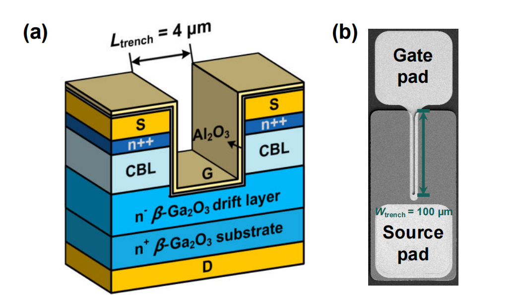
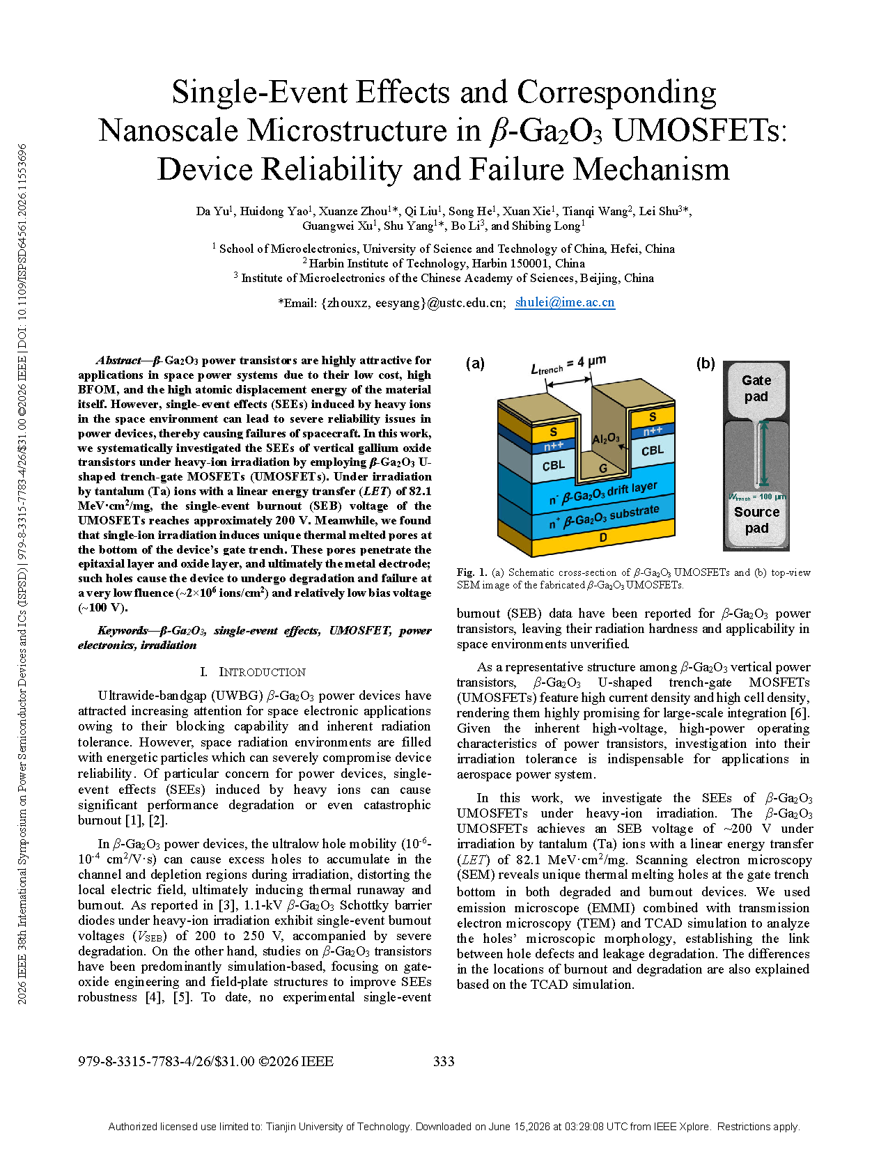
Fig. 1. (a) Schematic cross-section of β-Ga₂O₃ UMOSFETs and (b) top-view SEM image of the fabricated β-Ga₂O₃ UMOSFETs.
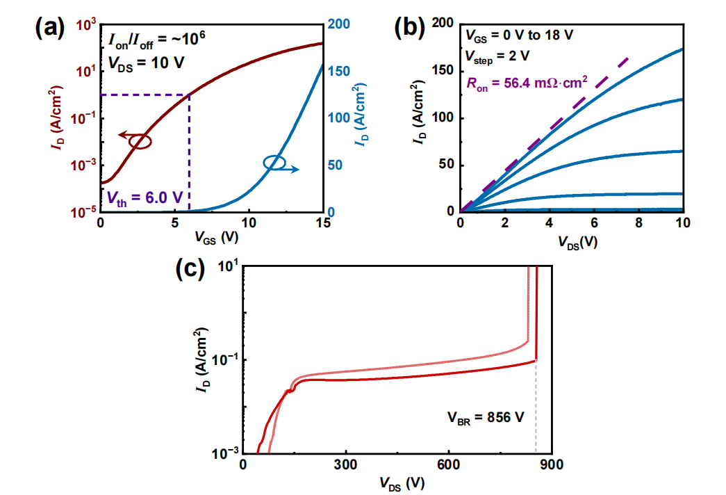
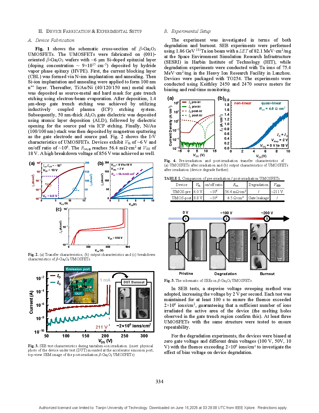
Fig. 2. (a) Transfer characteristics, (b) output characteristics and (c) breakdown characteristics of β-Ga₂O₃ UMOSFETs.
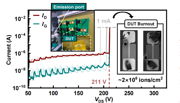
Fig. 3. SEB test characteristics during tantalum-ion irradiation. (inset: physical photo of the device under test (DUT) mounted at the accelerator emission port; top-view SEM image of the post-irradiation β-Ga₂O₃ UMOSFETs)
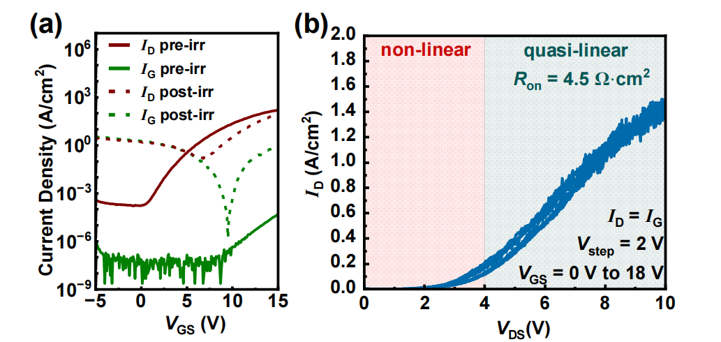
Fig. 4. Pre-irradiation and post-irradiation transfer characteristics of (a) UMOSFETs after irradiation and (b) output characteristics of UMOSFETs after irradiation (device degrade further).
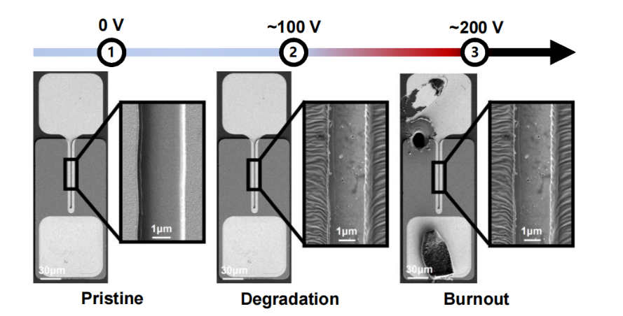
Fig. 5. The schematic of SEEs in β-Ga₂O₃ UMOSFETs.
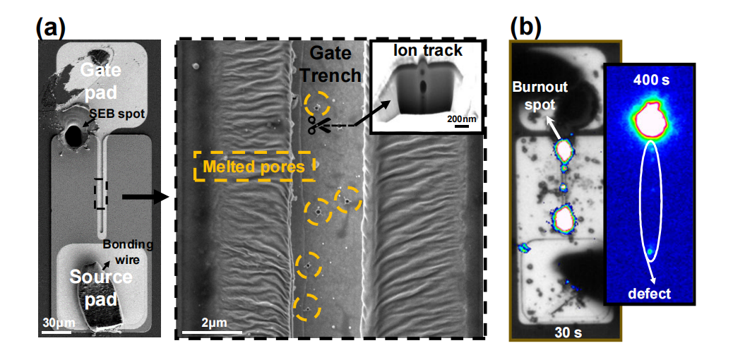
Fig. 6. (a) FIB-SEM characterization of the gate trench of post-irradiation β-Ga₂O₃ UMOSFETs: The pore in the trench is cross-sectioned via FIB, and its cross-sectional morphology was observed using SEM. (b) EMMI optical signal collection of post-irradiation β-Ga₂O₃ UMOSFETs under 50 V drain bias, week optical signals were captured after 30 s and 400 s of stress application, with distinct bright spots emerging in the gate trench.
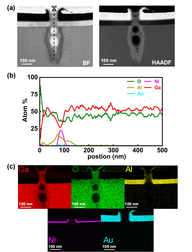
Fig. 7. (a) HAADF and BF images (acquired via TEM) of gate trench pores in UMOSFETs after irradiation-induced degradation and burnout. (b) EDS results along the radial direction of the pores. (c) EDS results of the entire pores.
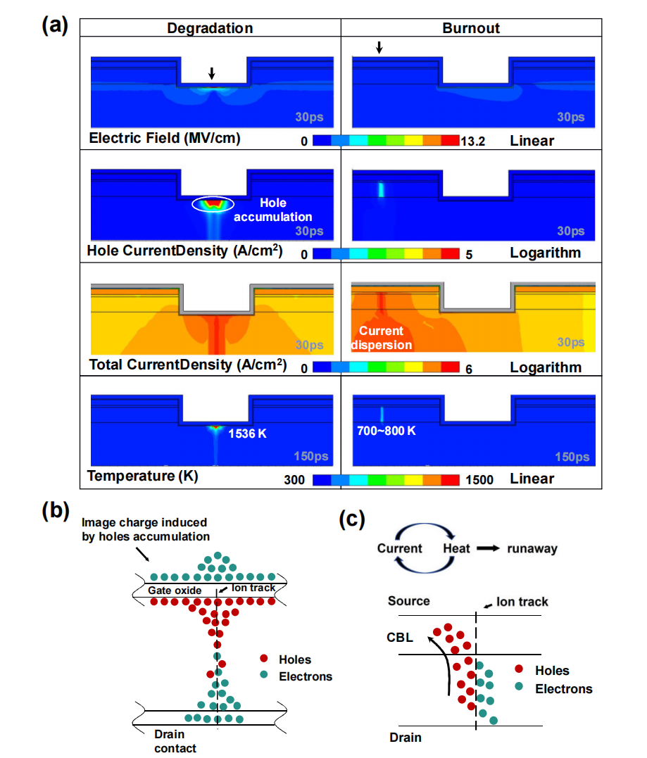
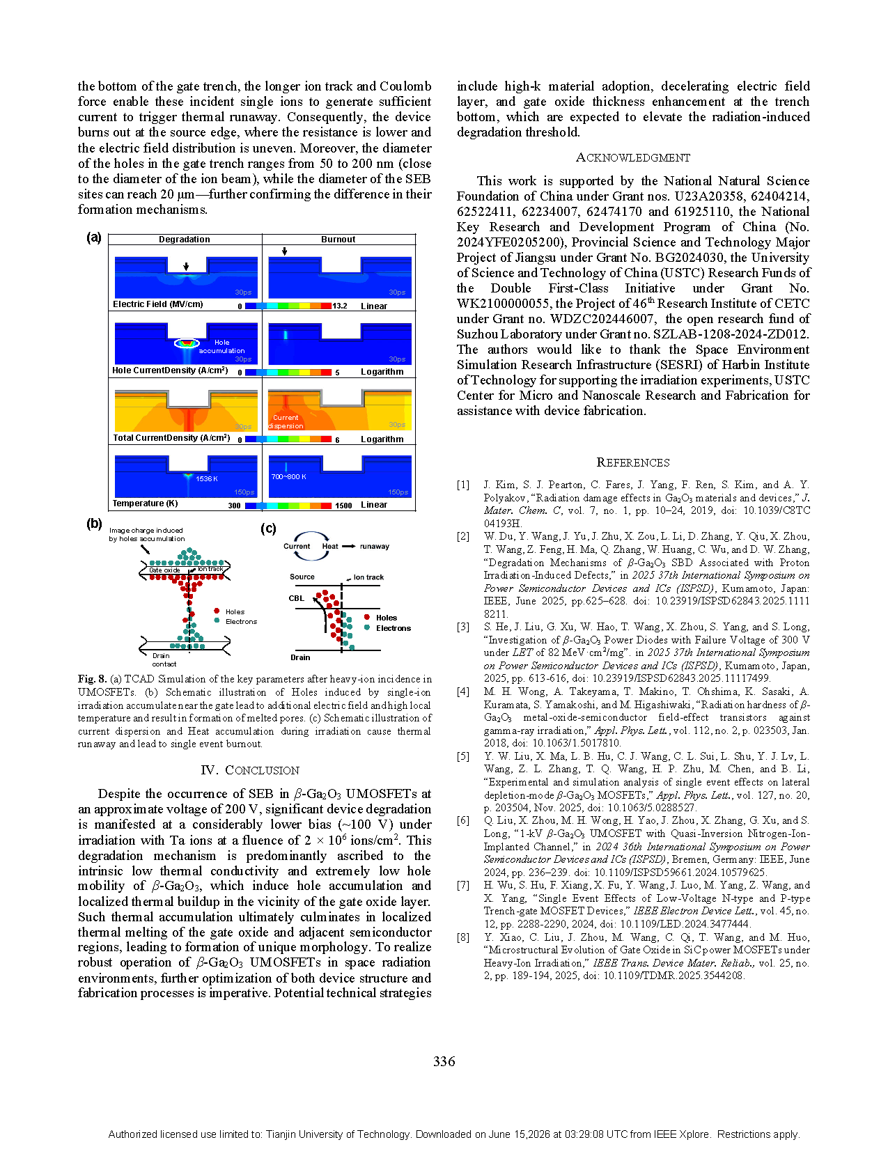
Fig. 8. (a) TCAD Simulation of the key parameters after heavy-ion incidence in UMOSFETs. (b) Schematic illustration of Holes induced by single-ion irradiation accumulate near the gate lead to additional electric field and high local temperature and result in formation of melted pores. (c) Schematic illustration of current dispersion and Heat accumulation during irradiation cause thermal runaway and lead to single event burnout.
DOI :
10.1109/ISPSD64561.2026.11553696