


Member News
Guangzhou Tanoxi Technology Showcases at FINE 2026 with Gallium Oxide Material Epitaxy and Device Fabrication Platform Enabling Next-Generation Power Semiconductor Applications
日期:2026-06-17阅读:45
Foreword
From June 10 to 12, 2026, the Future Industry New Materials Expo (FINE 2026) was held at the Shanghai New International Expo Centre. Guangzhou Tanoxi Technology Co., Ltd. showcased its Ga₂O₃ material epitaxy and device fabrication solutions at the Advanced Semiconductor Zone in Hall N1, engaging with professionals from power electronics, optoelectronics, new energy sectors, research institutes, and upstream/downstream industry partners.
As a semiconductor company focusing on gallium oxide (Ga₂O₃) epitaxial materials, customized epitaxial solutions, and device development, Tanoxi Technology aims to demonstrate the full technical pathway of Ga₂O₃—from material growth and process control to device fabrication—and further explore its application potential in high-voltage, high-efficiency power electronic systems.
Building Ga₂O₃ Device Capability Based on Epitaxial Materials
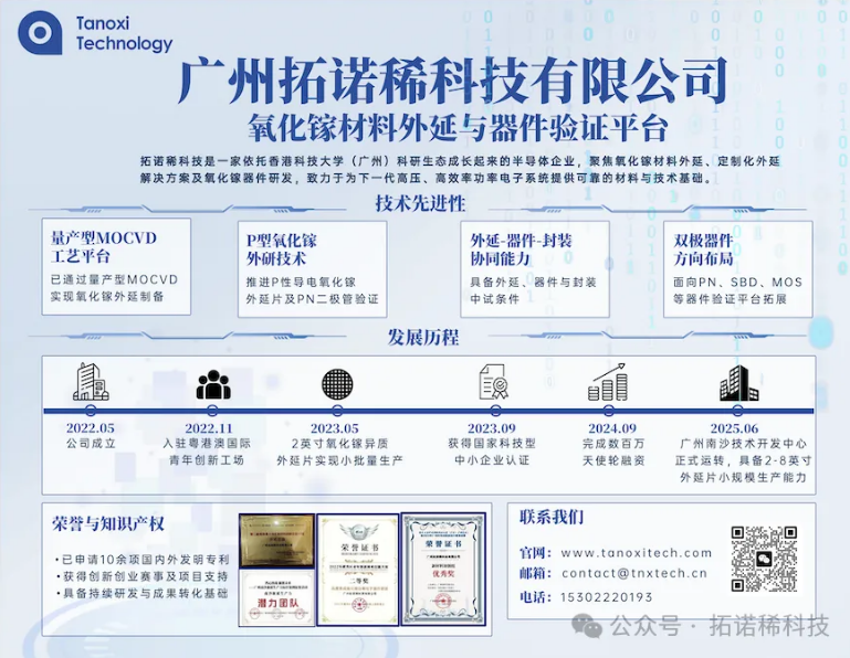
As an emerging ultra-wide bandgap semiconductor, gallium oxide has attracted increasing attention in power electronics and deep-UV optoelectronics.
Across its industrialization pathway, key challenges include material quality, epitaxial stability, doping control, and device fabrication processes—all of which directly determine final device performance and application potential.
Tanoxi Technology focuses on β-Ga₂O₃ epitaxy and continuously advances R&D and manufacturing, forming an integrated technical chain:
Epitaxial growth → Material characterization → Device fabrication → Performance validation
At FINE 2026, the company highlighted its “Ga₂O₃ material epitaxy and device fabrication platform,” showcasing progress in homoepitaxy, heteroepitaxy, Schottky barrier diode (SBD) devices, chips, and bare die fabrication.
Ga₂O₃ Product Portfolio Showcase
During the exhibition, Tanoxi Technology presented multiple Ga₂O₃ materials and devices, including:
10 mm × 10 mm β-Ga₂O₃ Homoepitaxial Wafers (P/N type)
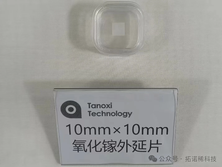
Based on β-Ga₂O₃ single-crystal substrates, these wafers serve as a key platform for high-quality homoepitaxial growth and device fabrication, enabling low-defect-density layers for power electronics and deep-UV optoelectronic applications.
2-inch Sapphire-based β-Ga₂O₃ Heteroepitaxial Wafers (P/N type)
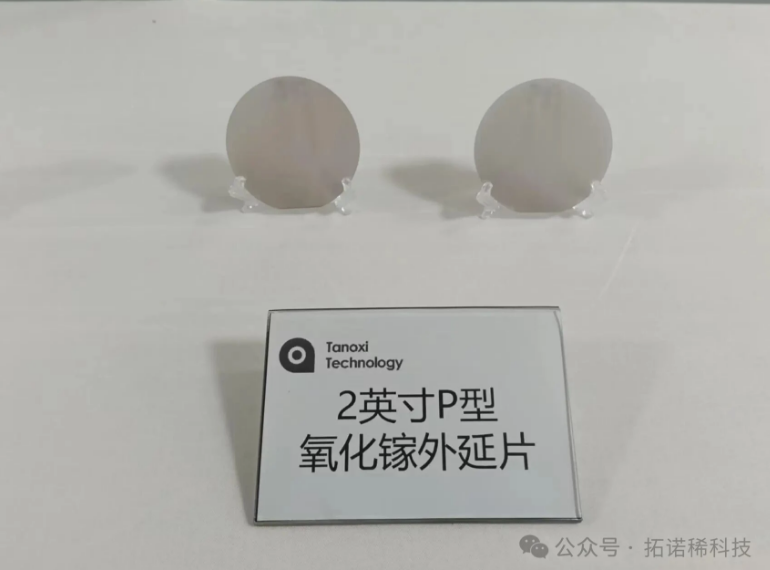
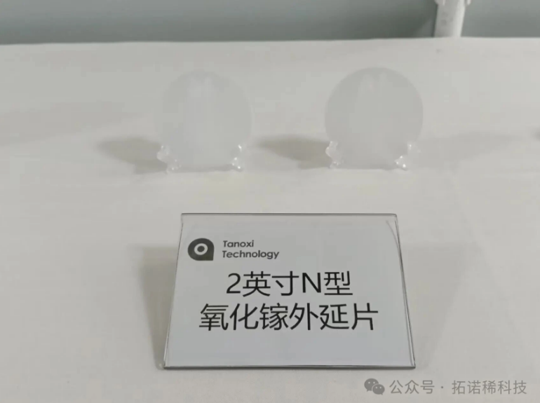
These wafers are grown on sapphire substrates, balancing crystal quality, substrate cost, and scalability. They are suitable for early-stage device research, process development, and application exploration.
Both P-type and N-type structures are included, providing a foundational platform for device architecture design.
4-inch Sapphire-based β-Ga₂O₃ Heteroepitaxial Wafers
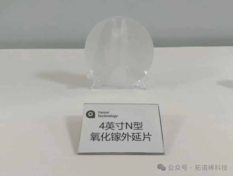
This product demonstrates the scalability of Ga₂O₃ heteroepitaxy toward larger wafer sizes and higher throughput, offering a pathway toward future large-scale device manufacturing.
Ga₂O₃-based Schottky Barrier Diodes (SBDs)
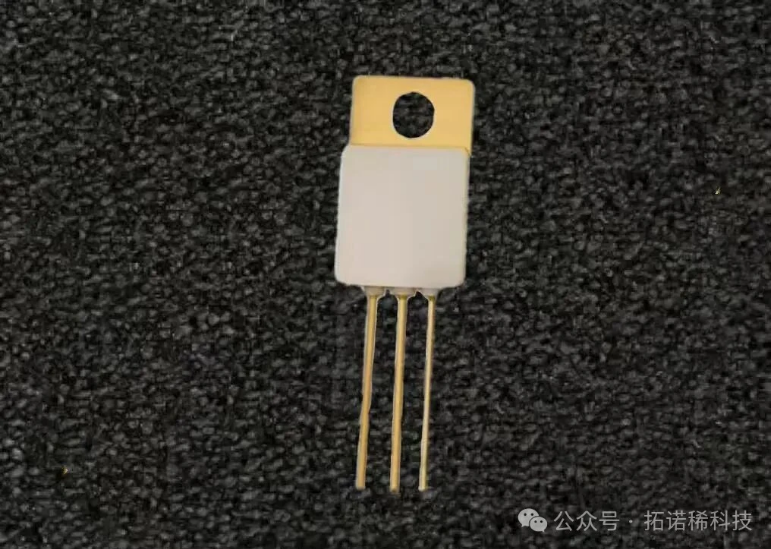
As a representative Ga₂O₃ power device, SBDs target high-voltage and high-frequency power conversion applications. Tanoxi’s SBD demonstration highlights the full chain capability from epitaxial materials to device fabrication and performance validation.
Ga₂O₃ PN Diodes
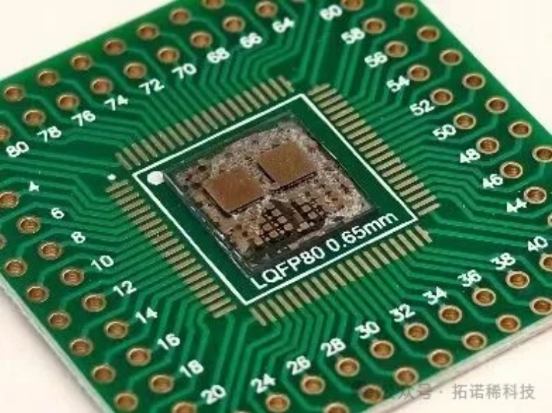
In addition to packaged devices, Ga₂O₃ PN diodes were also presented to demonstrate key achievements in device fabrication and to support process optimization, performance evaluation, and customer development needs.
Integrated Material–Device Solutions for Industry Applications
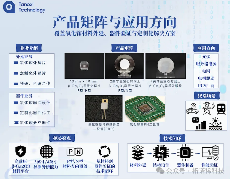
Tanoxi Technology currently focuses on two core business segments:
Epitaxy Services
Ga₂O₃ epitaxial wafers
Customized epitaxial solutions
R&D and collaborative development
Device Services
Ga₂O₃ device design
Foundry and fabrication services
Discrete Ga₂O₃ power devices
Through integrated material-device capabilities, the company aims to provide flexible material platforms, process support, and customized solutions for universities, research institutes, device manufacturers, and industry partners.
Expanding Application Horizons for Ga₂O₃
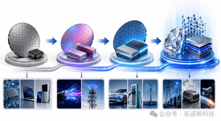
With growing demand for high-voltage, high-efficiency, and compact power electronics, Ga₂O₃ continues to show strong application potential.
During FINE 2026, discussions focused on applications including:
Solar power systems | Server power supplies | Power grids | Motor drives | PCS systems
Additionally, Ga₂O₃ is expected to play an important role in:
Electric vehicles | Smart grids | Rail transportation | 5G communications | Deep-UV optoelectronics
Conclusion
FINE 2026 provided a high-level platform for exchange among new materials, semiconductors, and advanced manufacturing sectors.
Through this exhibition, Tanoxi Technology demonstrated its progress in Ga₂O₃ epitaxial materials and device fabrication, while strengthening connections across the industrial ecosystem.
Looking forward, the company will continue investing in Ga₂O₃ epitaxy, device fabrication, and customized solutions, driving the transition of Ga₂O₃ from materials research to device-level applications and contributing to the development of next-generation power semiconductor technologies.
Contact
Guangzhou Tanoxi Technology Co., Ltd.
Website: www.tanoxitech.com
Email: contact@tnxtech.cn
