Paper Sharing
【Domestic Papers】High-Voltage Ga2O3 Schottky Barrier Diodes with Inserted Semi-Insulating Microcolumns for Suppression of Reverse Current
日期:2026-06-18阅读:43
Researchers from the Shenzhen University have published a dissertation titled "High-Voltage Ga2O3 Schottky Barrier Diodes with Inserted Semi-Insulating Microcolumns for Suppression of Reverse Current" in 2026 IEEE 38th International Symposium on Power Semiconductor Devices and ICs (ISPSD).
Background
Monoclinic β-Ga₂O₃, as a highly promising ultrawide-bandgap semiconductor material, possesses a bandgap of approximately 4.8-4.9 eV and a theoretical critical breakdown field of ~8 MV/cm. Moreover, low-cost, large-area single-crystal substrates can be obtained through melt growth methods, demonstrating broad application prospects in the field of high-voltage power devices. As a representative structure of gallium oxide power devices, Schottky barrier diodes (SBDs) often exhibit large reverse leakage current under high reverse bias due to the Schottky barrier lowering effect and related mechanisms, which severely limits their blocking capability.
To improve reverse characteristics, existing solutions mainly include reducing the carrier concentration in the drift layer or introducing structures such as JBS and trench MOS/MIS. However, these approaches each have significant limitations: reducing drift layer doping leads to a substantial increase in the difficulty of epitaxial growth control; JBS structures rely on p-type doping processes, while stable p-type doping technology in the gallium oxide system has not yet been matured; trench structures face challenges such as complex trench etching processes and high difficulty in high-k dielectric deposition. These issues are all unfavorable for process simplification and device reliability improvement. Therefore, developing a novel gallium oxide SBD structure with a simple process that can effectively suppress reverse leakage current has important academic value and engineering significance.
Abstract
This study develops a Ga₂O₃ inserted semi-insulating microcolumns Schottky barrier diodes (Ga₂O₃ IMC-SBDs) with a simple process flow and low reverse leakage current. The inserted microcolumns effectively reduce the interfacial electric field in the region near the Schottky junction and decrease the effective anode area of direct metal/semiconductor contact, thereby significantly suppressing the reverse leakage current. The fabricated Ga₂O₃ IMC-SBDs exhibits a reverse leakage current about two orders of magnitude lower than that of a conventional SBDs at V_R=1000 V, while maintaining a breakdown voltage of 1807 V, a specific on-resistance of 4.1 mΩ·cm², and a rectification ratio on the order of 10¹⁰. This structure provides a feasible solution for device design and process simplification of high-voltage, low-leakage β-Ga₂O₃ SBDs.
Highlights
Pioneering Semi-Insulating Microcolumn Structure: A semi-insulating microcolumn structure based on He-ion implantation is proposed and implemented for the first time. By precisely controlling the He-ion implantation depth and lateral distribution, high-resistivity semi-insulating microcolumns are locally formed in the anode region, eliminating the need for complex trench etching or p-type doping processes with a simple fabrication flow.
Dual Mechanism for Leakage Suppression: Semi-insulating microcolumns synergistically suppress reverse leakage current through two mechanisms: first, effectively reshaping the electric field distribution near the Schottky junction and reducing the electric field intensity at the metal/semiconductor interface; second, decreasing the effective anode area of direct metal-semiconductor contact and reducing potential leakage generation sites.
Systematic Verification of Material Mechanism: Combining SRIM simulation, first-principles calculations, XPS and UPS characterization, the physical mechanism by which He-ion implantation introduces acceptor-type defects such as VGa and Hei, transforming β-Ga₂O₃ from an n-type conductive state to a semi-insulating state, is systematically revealed.
Excellent Device Performance Trade-off: The fabricated Ga₂O₃ IMC-SBDs achieve a breakdown voltage of 1807 V and a specific on-resistance of 4.1 mΩ·cm². The leakage current at 1000 V reverse bias is two orders of magnitude lower than that of conventional SBDs, while maintaining a high rectification ratio of 10¹⁰, realizing a good balance between high-voltage blocking and low leakage.
Project Support
This study was financially supported by National Key Research and Development Program of China (2024YFE0205100), Guangdong Major Project of Basic and Applied Basic Research (2023B0303000012), Shenzhen Science and Technology Program (KJZD20240903102738050), and the Scientific Instrument Developing Project of ShenZhen University (Grant No.2024YQ003).
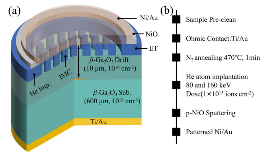
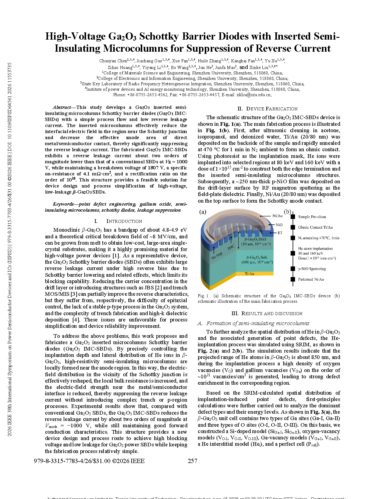
Fig. 1. (a) Schematic structure of the Ga₂O₃ IMC-SBDs device. (b) schematic illustration of the main fabrication process.
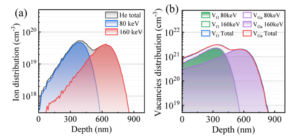
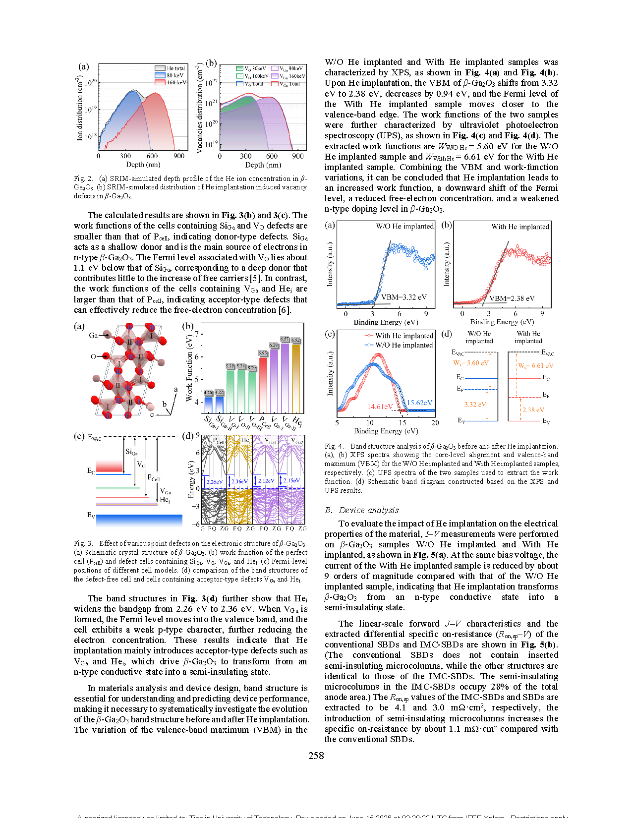
Fig. 2. (a) SRIM-simulated depth profile of the He ion concentration in β-Ga₂O₃. (b) SRIM-simulated distribution of He implantation induced vacancy defects in β-Ga₂O₃.
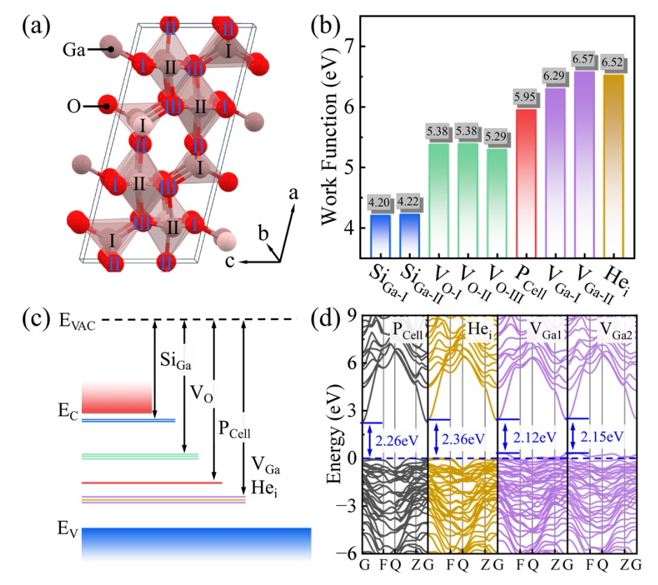
Fig. 3. Effect of various point defects on the electronic structure of β-Ga₂O₃ (a) Schematic crystal structure of β-Ga₂O₃. (b) work function of the perfect cell (Pcell) and defect cells containing SiGa, VO, VGa, and Hei. (c) Fermi-level positions of different cell models. (d) comparison of the band structures of the defect-free cell and cells containing acceptor-type defects VGa and Hei.
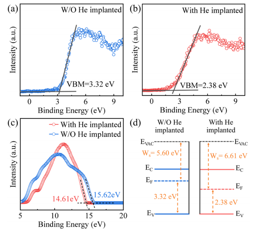
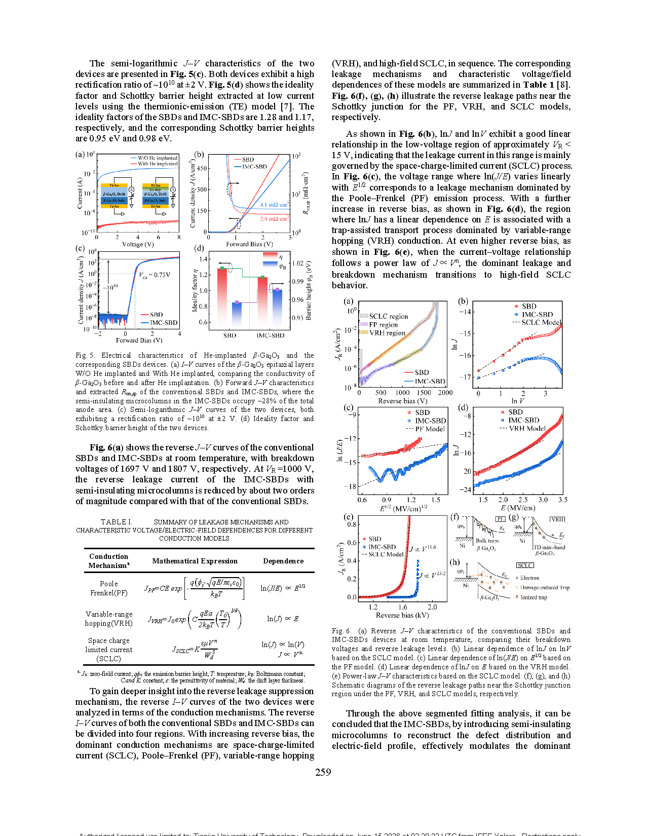
Fig. 4. Band structure analysis of β-Ga₂O₃ before and after He implantation. (a), (b) XPS spectra showing the core-level alignment and valence-band maximum (VBM) for the W/O He implanted and With He implanted samples, respectively. (c) UPS spectra of the two samples used to extract the work function. (d) Schematic band diagram constructed based on the XPS and UPS results.
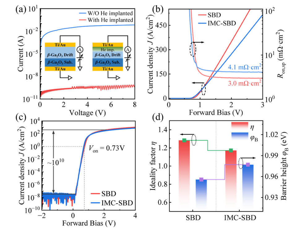
Fig. 5. Electrical characteristics of He-implanted β-Ga₂O₃ and the corresponding SBDs devices. (a) I-V curves of the β-Ga₂O₃ epitaxial layers W/O He implanted and With He implanted, comparing the conductivity of β-Ga₂O₃ before and after He implantation. (b) Forward J-V characteristics and extracted Ron,sp of the conventional SBDs and IMC-SBDs, where the semi-insulating microcolumns in the IMC-SBDs occupy ~28% of the total anode area. (c) Semi-logarithmic J-V curves of the two devices, both exhibiting a rectification ratio of ~1010 at ±2 V. (d) Ideality factor and Schottky barrier height of the two devices.
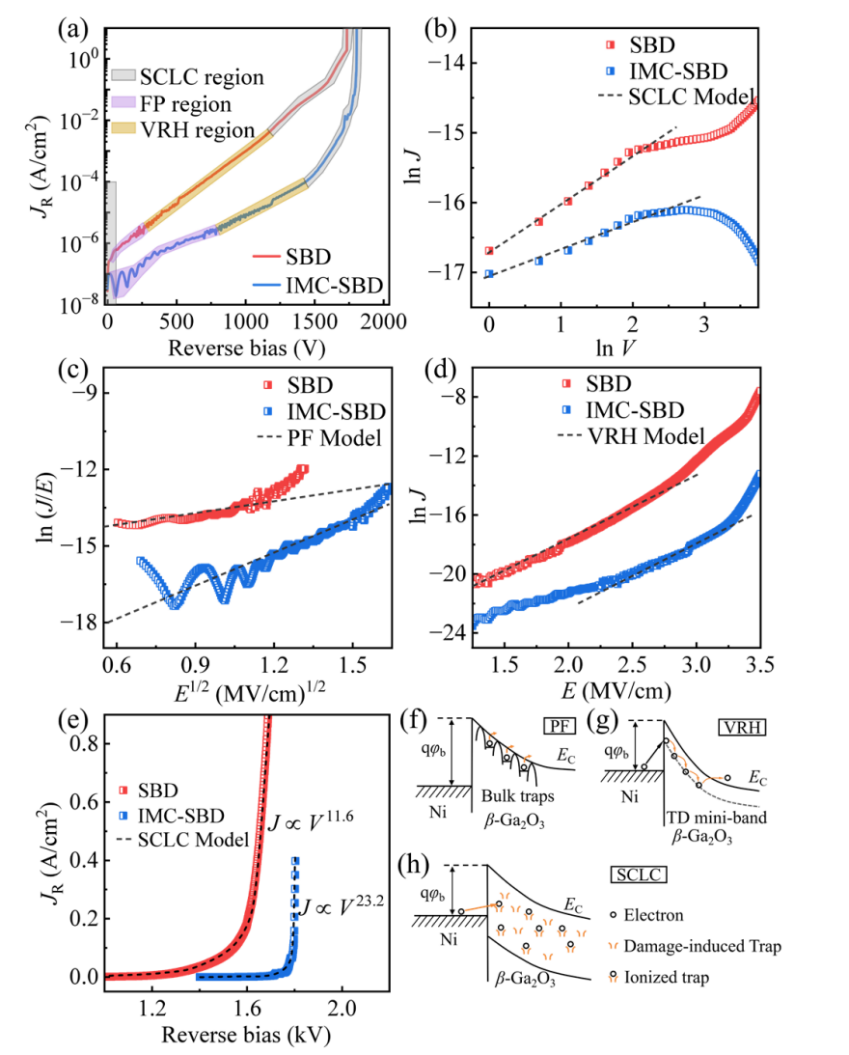
Fig. 6. (a) Reverse J-V characteristics of the conventional SBDs and IMC-SBDs devices at room temperature, comparing their breakdown voltages and reverse leakage levels. (b) Linear dependence of lnJ on lnV based on the SCLC model. (c) Linear dependence of ln (J/E) on E¹/² based on the PF model. (d) Linear dependence of lnJ on E based on the VRH model. (e) Power-law J–V characteristics based on the SCLC model. (f), (g), and (h) Schematic diagrams of the reverse leakage paths near the Schottky junction region under the PF, VRH, and SCLC models, respectively.
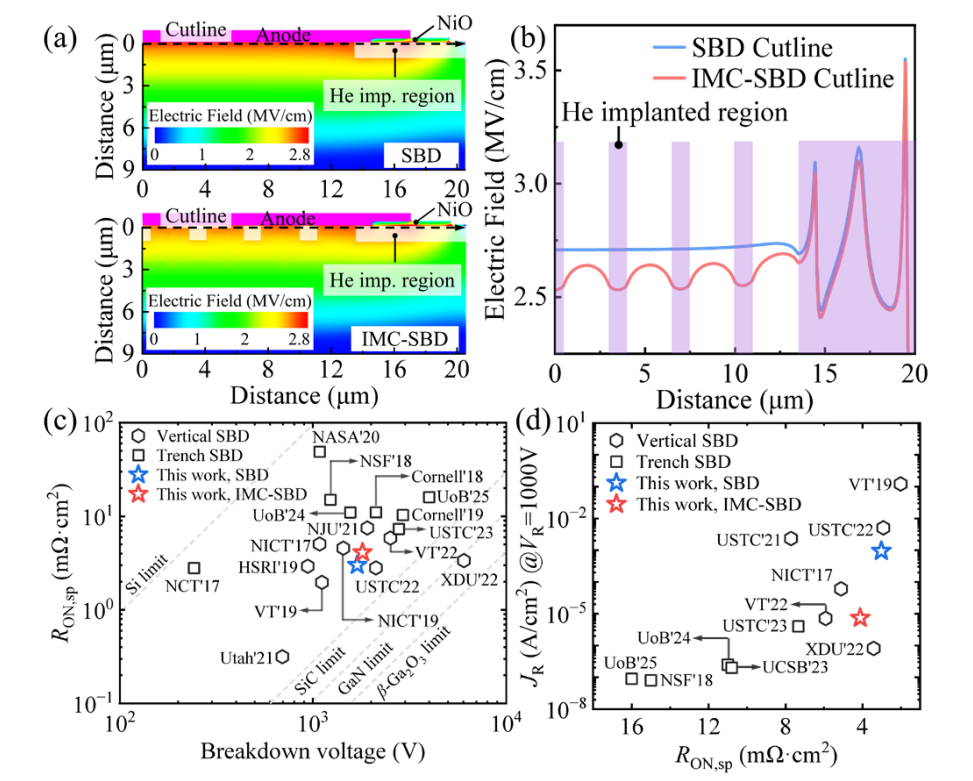
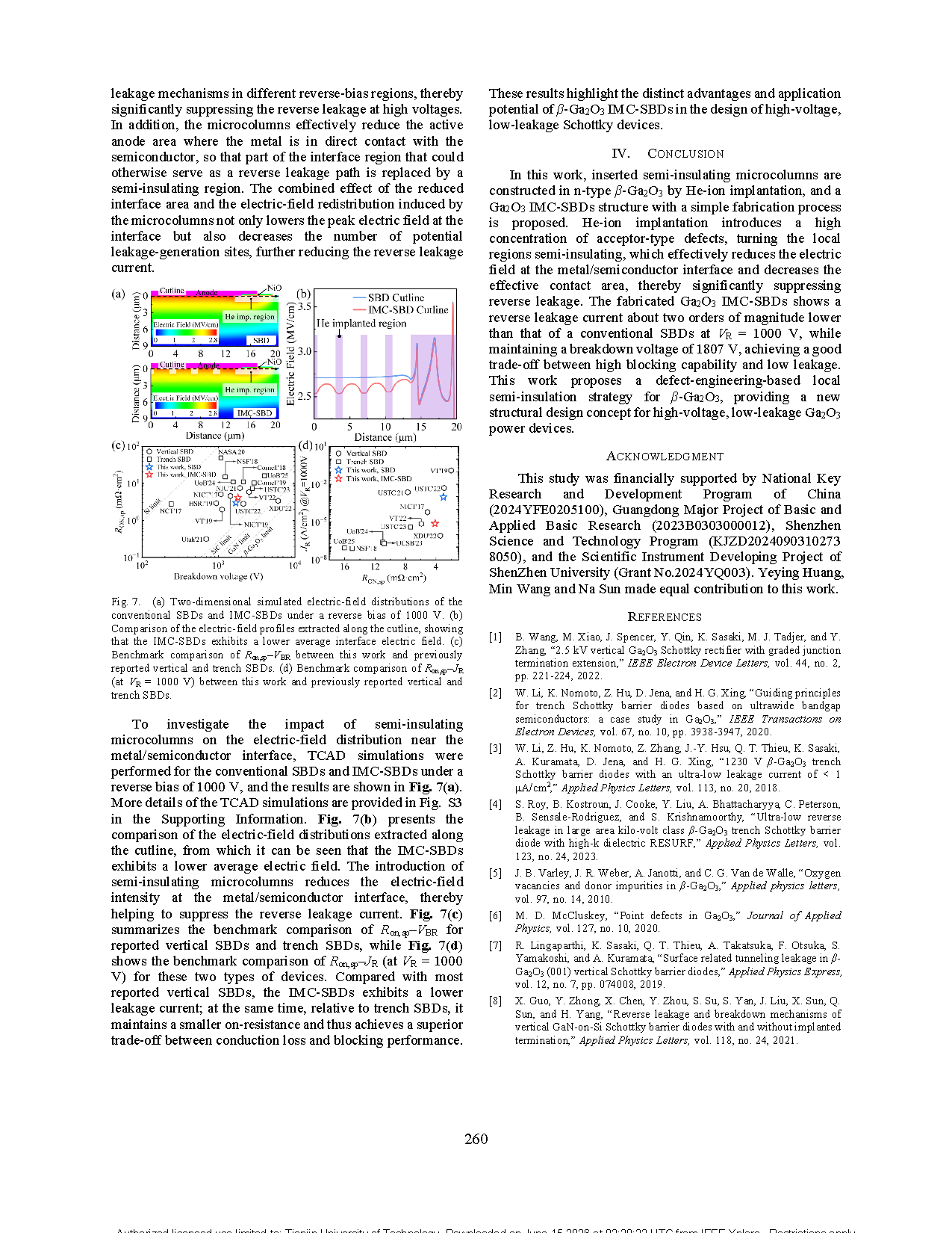
Fig. 7. (a) Two-dimensional simulated electric-field distributions of the conventional SBDs and IMC-SBDs under a reverse bias of 1000 V. (b) Comparison of the electric-field profiles extracted along the cutline, showing that the IMC-SBDs exhibits a lower average interface electric field. (c) Benchmark comparison of Ron,sp-VBR between this work and previously reported vertical and trench SBDs. (d) Benchmark comparison of Ron,sp-JR (at VR=1000 V) between this work and previously reported vertical and trench SBDs.
DOI :
10.1109/ISPSD64561.2026.11553735