


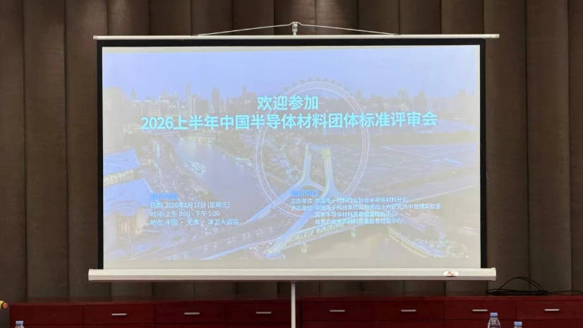
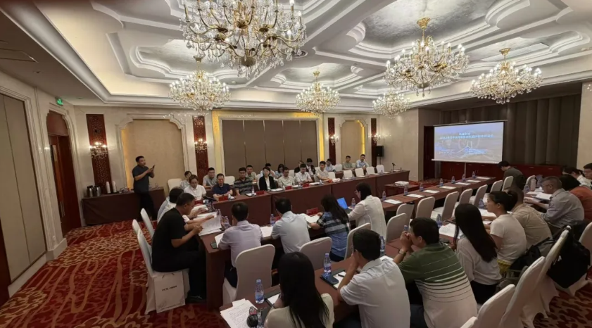
From June 16 to 17, the 2026 China Semiconductor Materials Group Standard Review Meeting (first half of the year) was held in Tianjin. The meeting was organized by the Semiconductor Materials Branch of the China Electronic Materials Industry Association, bringing together authoritative experts, leading enterprises, and research institutions in China’s semiconductor materials sector to conduct centralized reviews of multiple proposed group standards.
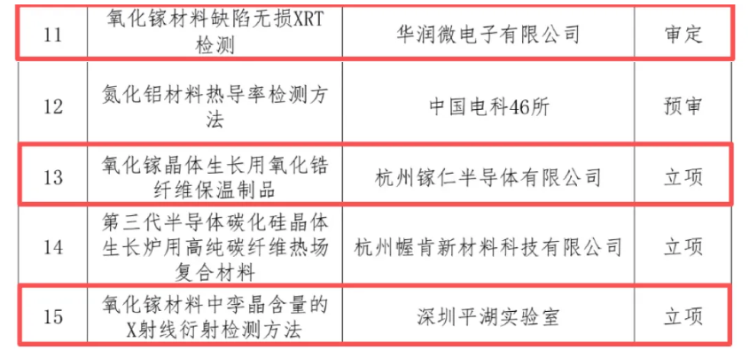
As a leading company in the fourth-generation semiconductor gallium oxide field, Hangzhou Garen Semiconductor Co., Ltd. (hereinafter referred to as “Garen Semiconductor”) led the initiation of the group standard “Zirconia Fiber Thermal Insulation Products for Gallium Oxide Crystal Growth”. The company also actively participated in the development of two additional standards: “Non-destructive XRT Inspection of Defects in Gallium Oxide Materials” and “X-ray Diffraction Method for Twin Content Measurement in Gallium Oxide Materials”. The parallel advancement of these three standards fully demonstrates Garen Semiconductor’s strong sense of corporate responsibility and its commitment to advancing industry standardization.
Zirconia fiber thermal insulation products are key thermal field materials used in the crystal growth process of gallium oxide. They feature excellent ultra-high-temperature resistance (up to 2400°C), outstanding thermal insulation performance, and high thermal stability without volatilization at elevated temperatures. These properties directly affect temperature gradient control and crystal quality stability during growth.
The group standard led by Garen Semiconductor will define classification, technical requirements, testing methods, and inspection rules for these products, aiming to establish a unified evaluation framework for thermal field materials and fill a domestic standardization gap in this field.
In May 2026, Garen Semiconductor signed a strategic cooperation agreement with Shandong Liangji Wendu New Materials Co., Ltd., further strengthening collaboration in materials R&D and thermal field design. The initiation of this group standard represents an important step for Garen Semiconductor in transforming its technical expertise into shared industry resources and promoting coordinated development across the supply chain.
In addition to its leading project, Garen Semiconductor is also actively involved in two gallium oxide-related standards.
The “Non-destructive XRT Inspection Method for Defects in Gallium Oxide Materials”, led by China Resources Microelectronics Co., Ltd., aims to establish a standardized non-destructive defect characterization method based on X-ray topography (XRT).
The “X-ray Diffraction Method for Twin Content Measurement in Gallium Oxide Materials”, led by Shenzhen Pingshan Laboratory, focuses on twins—a key defect affecting single-crystal quality and device performance—and promotes standardization of measurement methodologies.
In the development of both standards, Garen Semiconductor leverages its technical expertise in gallium oxide single-crystal growth to provide strong support for the scientific validity and practical applicability of the methods.
As a core leading enterprise in the fourth-generation gallium oxide semiconductor field, Garen Semiconductor relies on its in-house production lines and strong independent R&D capabilities. The company has achieved a globally leading technology platform featuring 8-inch gallium oxide substrates and 8-inch homoepitaxial wafers, establishing a full-chain capability covering equipment, crystal growth, substrates, and epitaxy.
Garen Semiconductor recognizes that leading enterprises must not only drive technological innovation but also take an active role in shaping industry standards. From leading two group standards—“β-phase Gallium Oxide Homoepitaxial Wafer” (T/CEMIA 050-2025) and “Test Method for Dislocation Density in Gallium Oxide Single Crystals” (T/CEMIA 051-2025)—to proposing two national standards, and now advancing a new round of group standards with a “1 leading, 2 participating” structure, Garen Semiconductor continues to contribute its technological strength to the standardization and healthy development of the gallium oxide industry.
The company will continue to uphold its mission of advancing standard system development and supporting high-quality industrial growth, contributing to a robust and sustainable industrial ecosystem.
Garen Semiconductor is committed to providing high-quality gallium oxide products and solutions. Its product portfolio includes VB crystal growth equipment dedicated to gallium oxide, commercial 6-inch gallium oxide homoepitaxial wafers, custom substrates for photoconductive switches, and 2-inch (011)-oriented gallium oxide substrates.
The company warmly welcomes partners across the industry chain to explore cooperation opportunities, jointly expand the application boundaries of gallium oxide in power electronics and optoelectronic devices, and accelerate the transformation of cutting-edge research into industry standards, thereby promoting the high-quality development of the gallium oxide sector.
About GAREN SEMI
Hangzhou Garen Semiconductor Co., Ltd. is a world-leading provider of Gallium Oxide materials and equipment solutions, focusing on R&D and industrialization in the ultra-wide bandgap semiconductor field. The company’s core products include 2–8-inch Gallium Oxide single crystals and substrates (with 8-inch being the world’s first), Gallium Oxide Vertical Bridgman (VB) crystal growth equipment, Gallium Oxide epitaxial wafers, etc. It is committed to building a full-chain product system of “equipment–crystal–substrate–epitaxy” to provide systematic solutions for global customers. The company’s achievements in Gallium Oxide have been specially reported by well-known media including People’s Daily, Xinhua News Agency, Science and Technology Daily, Sina Finance, China Blue News, and The Paper.
Enterprise Honors Summary
Recognized as a National-level Science and Technology Small and Medium-sized Enterprise and Zhejiang Innovative Small and Medium-sized Enterprise in 2023;Awarded Zhejiang Specialized, Sophisticated, Unique and New Small and Medium-sized Enterprise in 2024;Approved as a High-tech Enterprise in 2025;Won the SEMI Outstanding Contribution Award for Sustainable Development at SEMICON CHINA 2025, the Together Progress Award at the Jufeng Summit Forum (JFSC) and Compound Semiconductor Industry Expo, the Innovation Vitality Award of Zhejiang Semiconductor Industry, the Second Prize in the Enterprise Group of the 10th “Maker China” Zhejiang Provincial Finals, the Top 500 Enterprise Group of the 10th “Maker China” SME Innovation and Entrepreneurship Competition, and the 2024–2025 Semiconductor Material Industry Contribution Award;The major breakthrough in the preparation of 8-inch Gallium Oxide single crystals and substrates was selected as one of the “Top 10 Advances in China’s Third-Generation Semiconductor Technology 2025” and “Major Scientific and Technological Achievements 2025” by the Department of Science and Technology of Zhejiang Province;Led the formulation of 2 group standard drafts, participated in drafting 1 national standard, and participated in promoting 1 group standard draft in the Gallium Oxide field;Supported by the “5213” Excellence Program of Xiaoshan District, Hangzhou, Zhejiang Province, and approved to establish Zhejiang Enterprise Research Institute;Obtained the quality management system certification;Granted 20 authorized invention patents at home and abroad (including patents in the US, Japan and other countries), with more than 50 patents pending.
For more information about Garen Semiconductor and its products, please visit our official website: http://garen.cc/
Or contact us via the following ways:
Mr. Jiang: 15918719807
E-mail: jiangjiwei@garen.cc
Mr. Xia: 19011278792
E-mail: xianing@garen.cc
Instruction
Official Account

Cooperation
Top
