


According to a report by China Economic Times, at the 2023 China Optical Valley Jiufengshan Forum and Compound Semiconductor Industry Conference, Academician Hao Yue of the Chinese Academy of Sciences stated that although oxide semiconductors still have some distance to go before large-scale industrial application, their broad application prospects are already clearly visible. Compared with gallium nitride (GaN) and silicon carbide (SiC), oxide semiconductors possess a wider bandgap, theoretically enabling lower conduction losses. However, heat dissipation remains a core bottleneck constraining their industrialization.
Device-level electro-thermal characteristics and reliable physical data constitute an important prerequisite for constructing self-consistent electro-thermal coupling models of ultrawide bandgap (UWBG) semiconductor power devices, conducting steady and transient-state electro-thermal numerical simulations, and performing electro-thermal co-design optimization. Associate Professor Li Yuan from the Faculty of Integrated Circuits at Xidian University has long focused on this critical scientific challenge. Targeting the core issue of device overheating that hinders the maturation of β-Ga₂O₃ power device technology, she has systematically overcome several key characterization and modeling technologies: time-domain thermo-reflectance (TDTR) optical characterization for precise extraction of unknown thermal properties of β-Ga₂O₃ devices, transient thermal imaging (TTI) thermo-reflectance imaging for complex transient electro-thermal characterization of β-Ga₂O₃ devices, and forward physical modeling of β-Ga₂O₃ device electro-thermal coupling integrating material,device and package analysis. On this basis, she has conducted a series of studies on electro-thermal co-design and thermal management system technologies for β-Ga₂O₃ MOS-type trench diodes, MOSFETs, and other devices, establishing a high-precision research framework for electro-thermal coupling modeling and co-optimization design of ultrawide bandgap semiconductor power devices.
Her representative research include:
An Electro-Thermal Co-Designed Ga₂O₃ [100] Trench Power Diode Featuring Ferroelectric Dielectric
Electro-Thermal Co-Design β-Ga₂O₃ MOS-Type Trench Diode Based on Optimized Trench-Sidewall Interface Quality Strategy and Mechanism Study
Implications for FD-OSIQ-Based Electrothermal Co-Design: Degradation of Reverse Performance in β-Ga₂O₃ Ferroelectric Trench Diodes Under Forward-Voltage Stress
Electro-Thermal Improvement in a β-Ga₂O₃ Cage-Integrated Slanted-Fin MOSFET
The Diamond-Plate Double-Side-Cooled β-Ga₂O₃ SBD Prototype with an Ultra-Low RθJC of 0.24 K/W
This series of work breaks through the limitations of traditional single-physics-field design by deeply integrating the coupling mechanisms of electrical and thermal domains. It systematically reveals the physical mechanisms of electro-thermal-field interactions in β-Ga₂O₃ devices under steady- and transient- conditions, providing important theoretical support for device structure optimization, electro-thermal co-design, and improved operational robustness. The established research framework holds significant theoretical value and guiding importance for advancing the engineering application and industrialization of ultrawide bandgap semiconductor power devices.
The following is a report on the first work of this series.
Researchers from Xidian University have published a dissertation titled " An Electro-Thermal Co-Designed Ga₂O₃ [100] Trench Power Diode Featuring Ferroelectric Dielectric " in The 35th International Symposium on Power Semiconductor Devices and ICs(ISPSD 2023).
Background
Recently, β-phase gallium oxide (Ga₂O₃) has emerged as a primary candidate to enable next-generation power devices. Aside from the mass producible melt-grown substrates and the existence of shallow donors, the very high Baliga’s figure of merit (BFOM) benefited from the large breakdown electric field, even beyond the values of traditional wide bandgap semiconductors such as 4H-SiC (10×) and GaN (4×). A trench metal-insulator-semiconductor (MIS) structure successfully realized in Si and SiC is a desirable candidate for β-Ga₂O₃ diodes, which gets benefit from the 2-D or 3-D electric-field profile and effectively alleviates the constraint due to the leakage current (JR) induced by the surface field effect of Ga₂O₃ Schottky barrier diodes (SBDs). Recently, kilovolt-class Ga₂O₃ MOS-type trench SBDs were demonstrated. Now, one major roadblock toward the maturation of Ga₂O₃ technology is device overheating. Because of the low symmetry nature of β-Ga₂O₃, the kT of the different rotated trench sidewalls is different. Although with the higher kT[010] of [100] trench sidewall compared to [010] trench sidewall, the Ga₂O₃ trench devices with [100] trench are rarely adopted, due to the worst sidewall interface quality induced by sidewall-orientation-dependent etch damage, even after the wet etch repair using acids. Optimized sidewall interface quality (OSIQ) of the trench is not only preferred, but also urgently necessary for comprehensive improvement of electro-thermal performance of Ga₂O₃ trench device.
Abstract
One major roadblock toward the maturation of Ga₂O₃ technology is device overheating. For Ga₂O₃ trench devices, although with the higher thermal conductivity (kT[010]) of [100] trench sidewall compared to [010] trench sidewall, the Ga₂O₃ trench devices with [100] trench are rarely adopted, due to the worst sidewall interface quality induced by sidewall orientation-dependent etch damage, even after the wet etch repair using acids. For the first time, the proposed electro thermal co-designed Ga₂O₃ [100] trench diode based on optimized trench sidewall interface quality, featuring ferroelectric dielectric, exhibits better performance compared with Ga₂O₃ [010] trench diode. Under the identical power consumption, the Ga₂O₃ [100] trench diode shows the lowest center junction temperature, which is 9 degree lower than that of Ga₂O₃ [010] trench diode. The new interface-quality optimization strategy can significantly provide potential for electro-thermal optimization of Ga₂O₃ trench devices.
Conclusion
For the first time, the presented electro-thermal co designed Ga₂O₃ [100]TD, featuring ferroelectric dielectric, exhibits better performance compared with [010]TD, which provides great potential for design optimization of Ga₂O₃ trench devices.
Project Support
This work was supported by the NSFC under Grant Nos. 62204187.
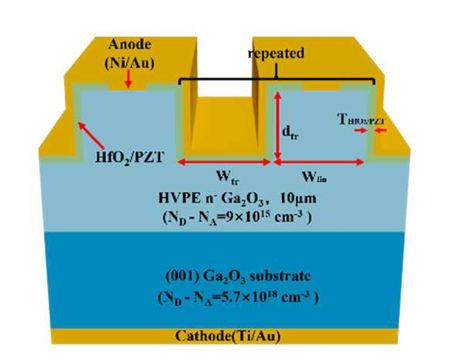
Fig. 1. Schematic cross section of the Trench Diodes.
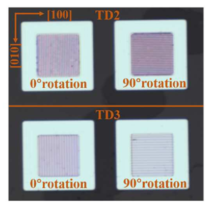
Fig. 2. The image of TDs with trench along the [010] direction (0° rotation) and trench along the [100] direction (90° rotation).
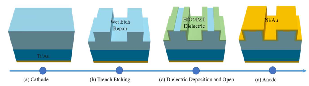
Fig. 3. Fabrication process flow of Ga₂O₃ trench diode.
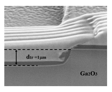
Fig. 4. Scanning electron microscopy image of trench depth (dtr) of 1 µm.
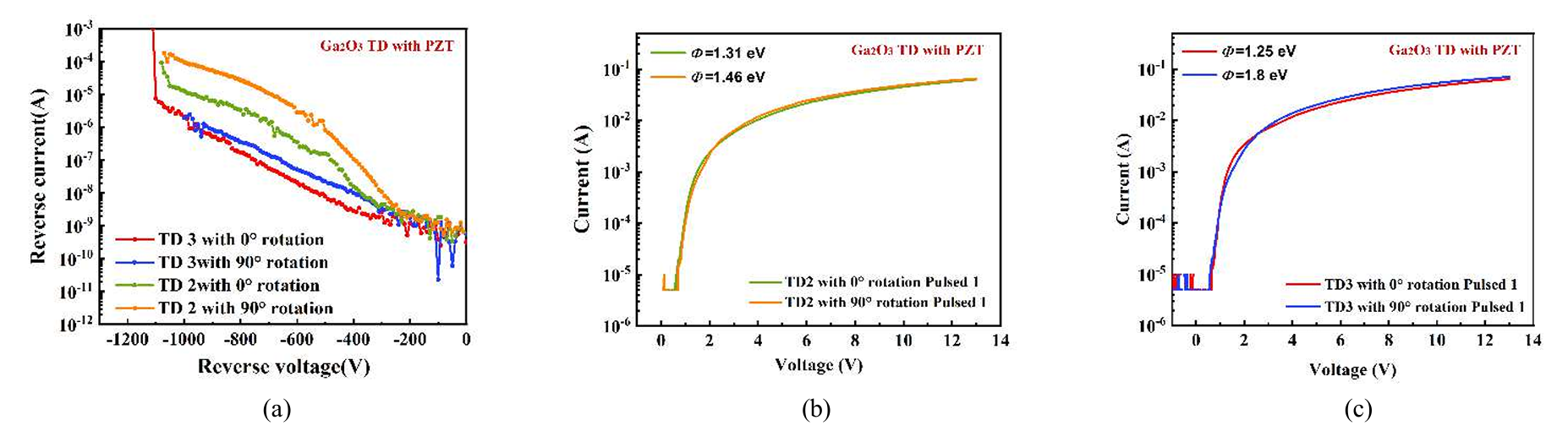
Fig. 5. (a) Reverse bias I-V characteristics of PZT TD2&3. (b) Forward I-V characteristics of PZT TD2 with 0° rotation and 90°rotation under pulsed measurement respectively. (c) Forward I-V characteristics of PZT TD3 0° rotation and 90° rotation under pulsed measurement respectively.
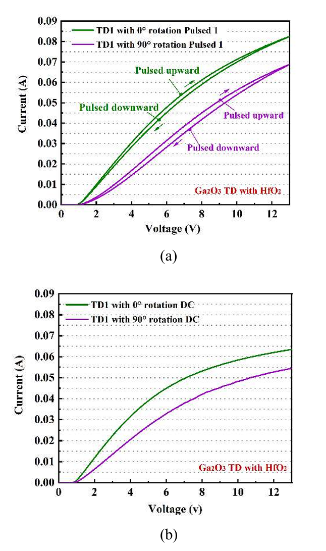
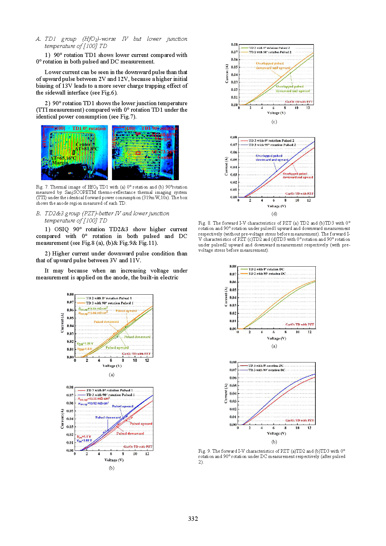
Fig. 6. (a) Forward I-V characteristics of HfO2 TD1 with 0° rotation and 90° rotation under pulsed upward and pulsed downward measurement respectively. (b) Forward I-V characteristics of HfO2 TD1 with 0° rotation and 90° rotation under DC measurement.
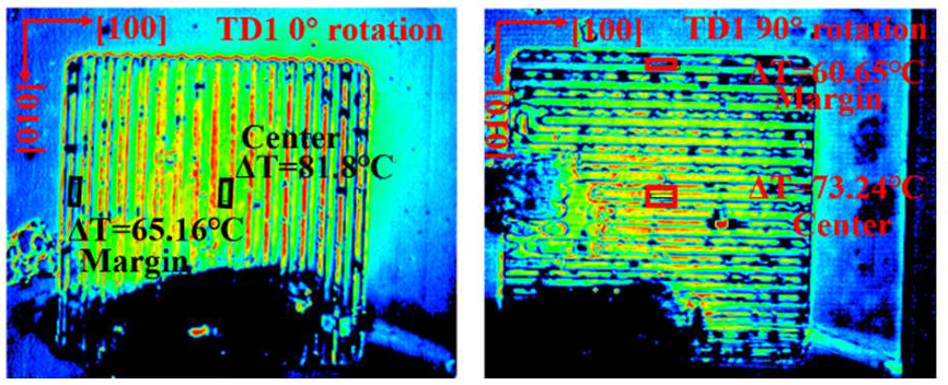
Fig. 7. Thermal image of HfO2 TD1 with (a) 0° rotation and (b) 90°rotation measured by SanjSCOPETM thermo-reflectance thermal imaging system (TTI) under the identical forward power consumption (319 mW,10s). The box shows the anode region measured of each TD.
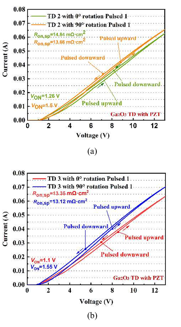
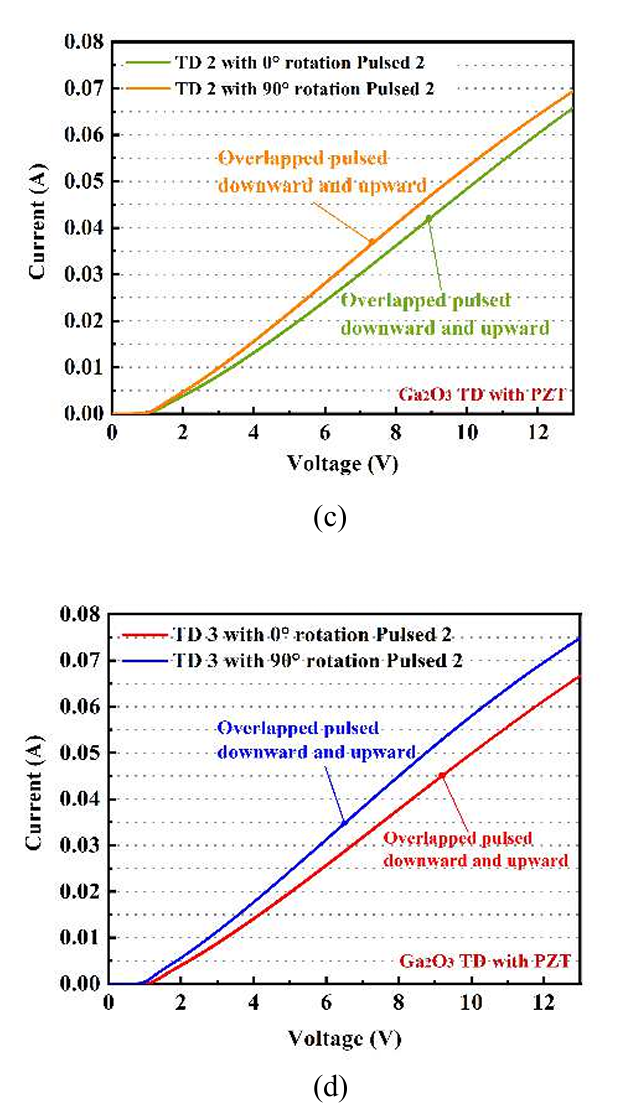
Fig. 8. The forward I-V characteristics of PZT (a) TD2 and (b)TD3 with 0° rotation and 90° rotation under pulsed1 upward and downward measurement respectively (without pre-voltage stress before measurement). The forward IV characteristics of PZT (c)TD2 and (d)TD3 with 0° rotation and 90° rotation under pulsed2 upward and downward measurement respectively (with prevoltage stress before measurement).
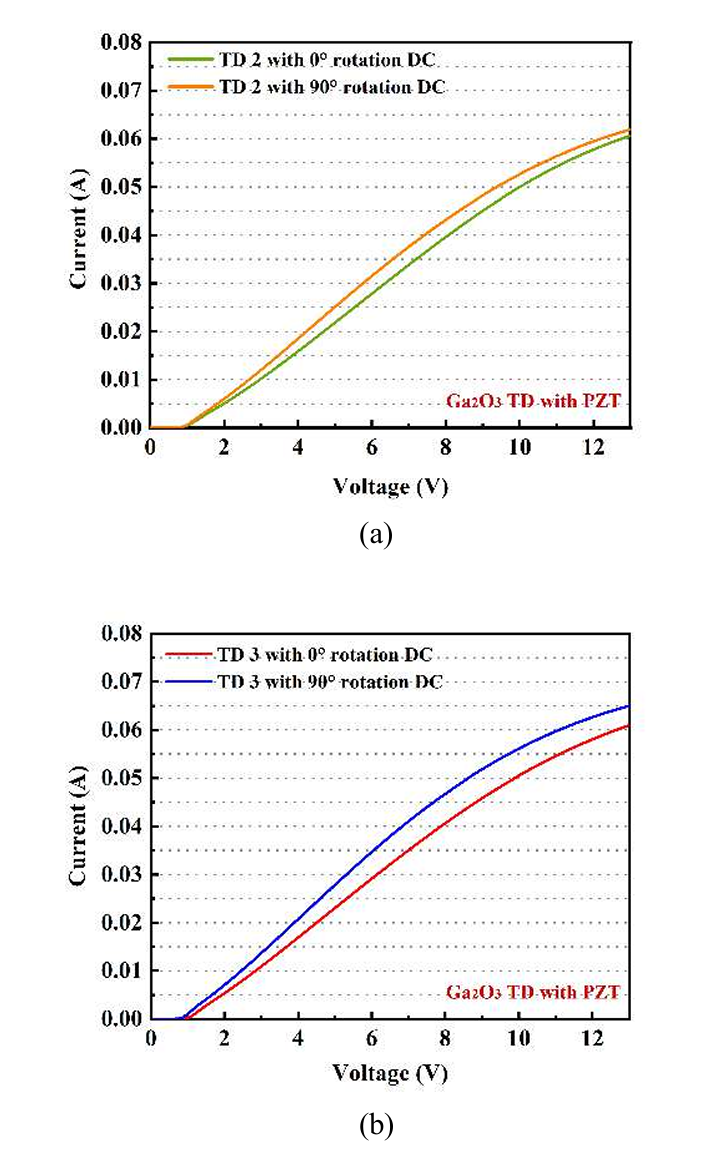
Fig. 9. The forward I-V characteristics of PZT (a)TD2 and (b)TD3 with 0° rotation and 90° rotation under DC measurement respectively (after pulsed 2).
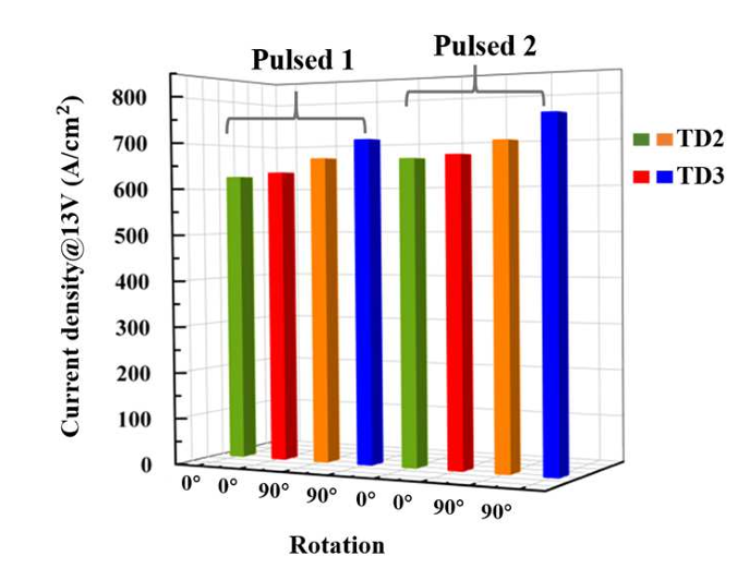
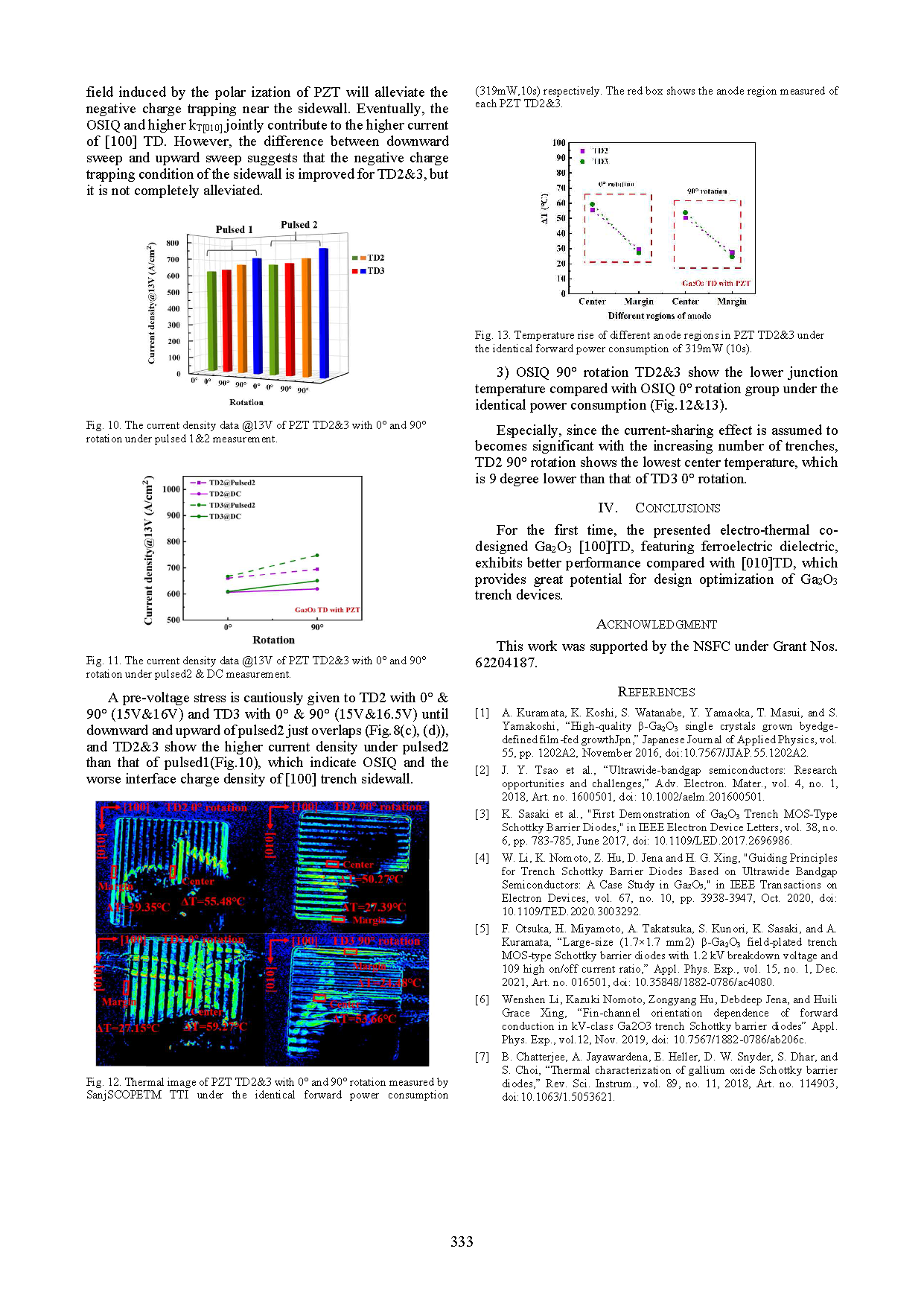
Fig. 10. The current density data @13V of PZT TD2&3 with 0° and 90° rotation under pulsed 1&2 measurement.
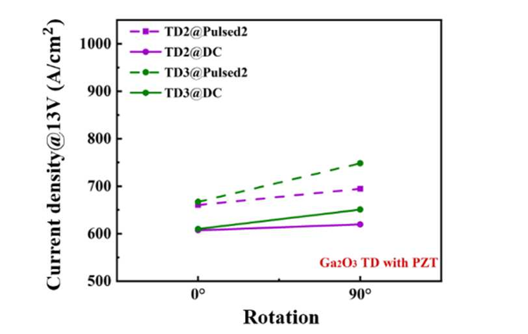
Fig. 11. The current density data @13V of PZT TD2&3 with 0° and 90° rotation under pulsed2 & DC measurement.
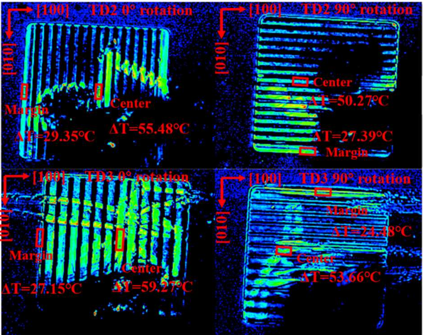
Fig. 12. Thermal image of PZT TD2&3 with 0° and 90° rotation measured by SanjSCOPETM TTI under the identical forward power consumption (319 mW,10s) respectively. The red box shows the anode region measured of each PZT TD2&3.
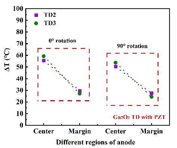
Fig. 13. Temperature rise of different anode regions in PZT TD2&3 under the identical forward power consumption of 319 mW (10s).
DOI:
10.1109/ISPSD57135.2023.10147506
Instruction
Official Account

Cooperation
Top
