


Researchers from the Shanghai University & Ningbo Institute of Materials Technology and Engineering, Chinese Academy of Sciences have published a dissertation titled "High Breakdown Voltage (>3 kV) in β-Ga₂O₃ Lateral MOSFETs Enabled by a Si₃N₄ Terminal Structure" in Electronics.
Background
The ultra-wide-bandgap semiconductor β-Ga₂O₃ has a bandgap of approximately 4.8 eV and a theoretical critical electric field of 8 MV/cm, far exceeding that of SiC and GaN, making it a promising candidate for high-voltage power devices. Large-area and high-quality native substrates of β-Ga₂O₃ can be fabricated via melt-grown techniques, which supports low-cost large-scale production. Lateral MOSFETs are suitable for planar processing and allow independent optimization of drift regions, showing great potential for power integration. However, electric field crowding at the gate edge of lateral β-Ga₂O₃ MOSFETs easily causes premature avalanche breakdown and dielectric failure, severely restricting the device breakdown performance.
Existing solutions including field plates, reduced surface field structures and high-k dielectric passivation layers have obvious drawbacks. Field plates increase parasitic capacitance and fabrication complexity, RESURF structures require precise doping control, and conventional passivation layers cannot effectively relieve field crowding without degrading on-state performance. Hence, it is urgent to develop a simple, process-compatible electric field management strategy to simultaneously improve breakdown voltage and maintain excellent forward conduction characteristics for β-Ga₂O₃ power devices.
Abstract
We report a lateral β-Ga₂O₃ MOSFET incorporating a simple Si₃N₄ terminal structure for electric-field management. The main contribution of this work is the demonstration that this process-compatible terminal design can enhance the breakdown performance while preserving the forward conduction characteristics of the device. The epitaxial layer exhibits high crystalline quality, a smooth surface morphology, and favorable carrier transport properties. With the Si₃N₄ terminal structure, the device achieves a breakdown voltage exceeding 3 kV, and the average breakdown field is increased from 0.85 MV/cm to 1.63 MV/cm. Meanwhile, the forward conduction characteristics are well maintained. Electric-field simulations further reveal that the Si₃N₄ terminal structure effectively mitigates electricfield crowding at the gate edge, accounting for the improved breakdown behavior. These results demonstrate that the Si₃N₄-based terminal design provides a simple and effective strategy for simultaneously improving breakdown performance and maintaining forward conduction characteristics in lateral β-Ga₂O₃ MOSFETs.
Highlights
A simple and process-compatible Si₃N₄ terminal structure is proposed to relieve electric field crowding at the gate of lateral β-Ga₂O₃
The device breakdown voltage exceeds 3 kV, and the average breakdown field is nearly doubled, realizing remarkable improvement of high-voltage resistance.
The Si₃N₄ terminal structure causes no degradation to device conduction performance, and key parameters such as saturation drain current density and specific on-resistance remain excellent.
Electric field simulations verify the electric field homogenization mechanism, offering a new design strategy for β-Ga₂O₃ high-voltage power devices.
Conclusion
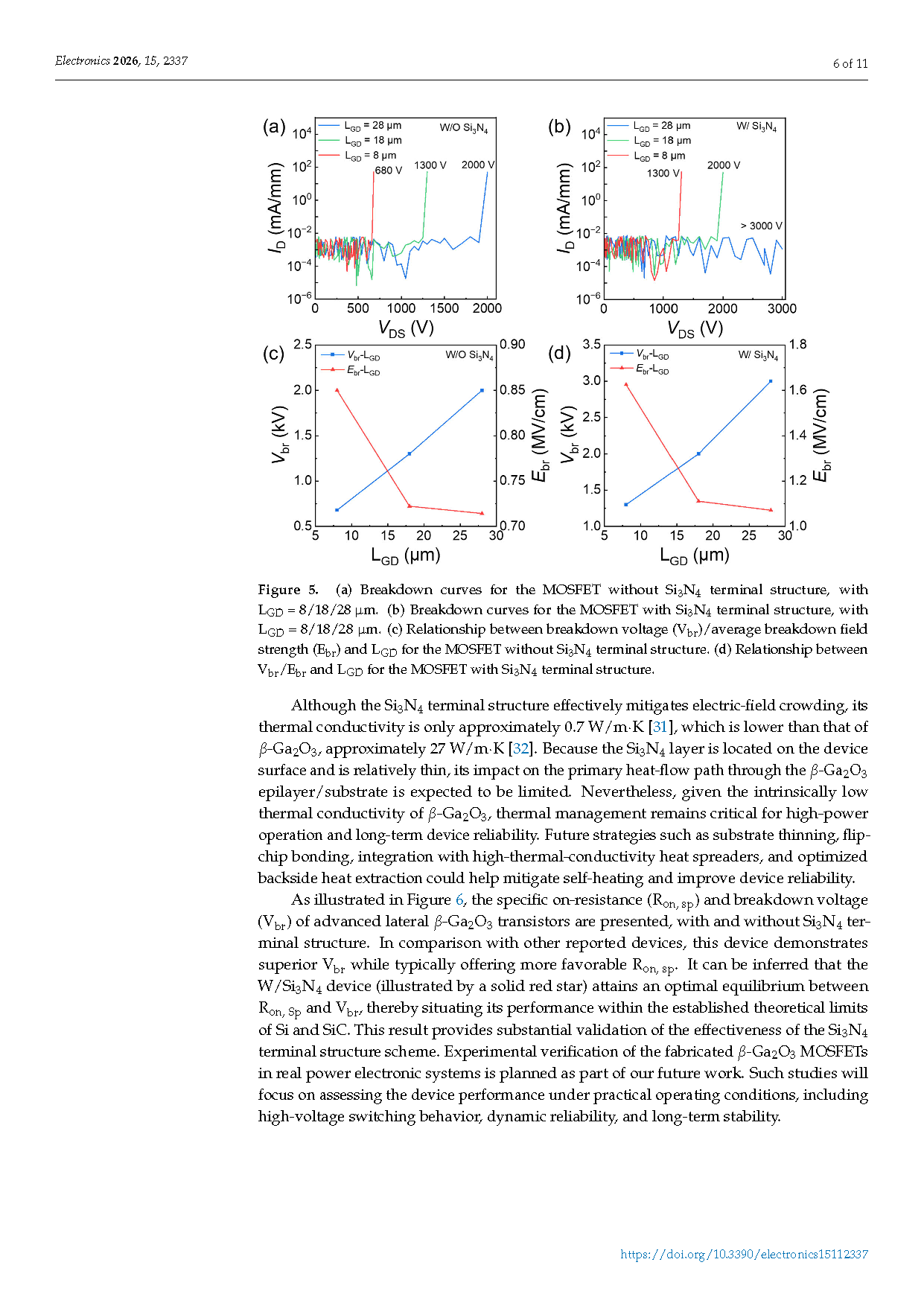
We demonstrate a lateral β-Ga₂O₃ MOSFET with a Si₃N₄ terminal structure that achieves a breakdown voltage surpassing 3 kV. After the introduction of the Si₃N₄ terminal structure, the device does not compromise the on-state device performance, with Vₜₕ=−31.75 V, SS=701.42 mV/dec, ID,sat=61.65 mA/mm and Rₒₙ,ₛₚ=165.44 mΩ·cm². For LGD=8,18,and 28 μm, the breakdown voltages increase from 680, 1300, and 2000 V to 1300, 2000, and over 3000 V, respectively. The average breakdown field is enhanced from 0.85 to 1.63 MV/cm. Electric field simulations confirm that this improvement originates from the mitigation of electric field crowding at the gate edge by the Si₃N₄ terminal structure. Collectively, these results demonstrate that the Si₃N₄ terminal design provides a simple and effective approach to improving the high-voltage performance of lateral β-Ga₂O₃ MOSFETs. Future work will focus on thermal optimization, dynamic reliability evaluation, and experimental verification in practical power electronic systems.
Project Support
This research was funded by the National Natural Science Foundation of China, grant number 62204244 and the Zhejiang Provincial Natural Science Foundation of China, grant number LQ23F040003 and the Ningbo Yongjiang Talent Introduction Programme, grant number 2021A-046-C.
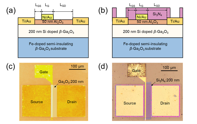
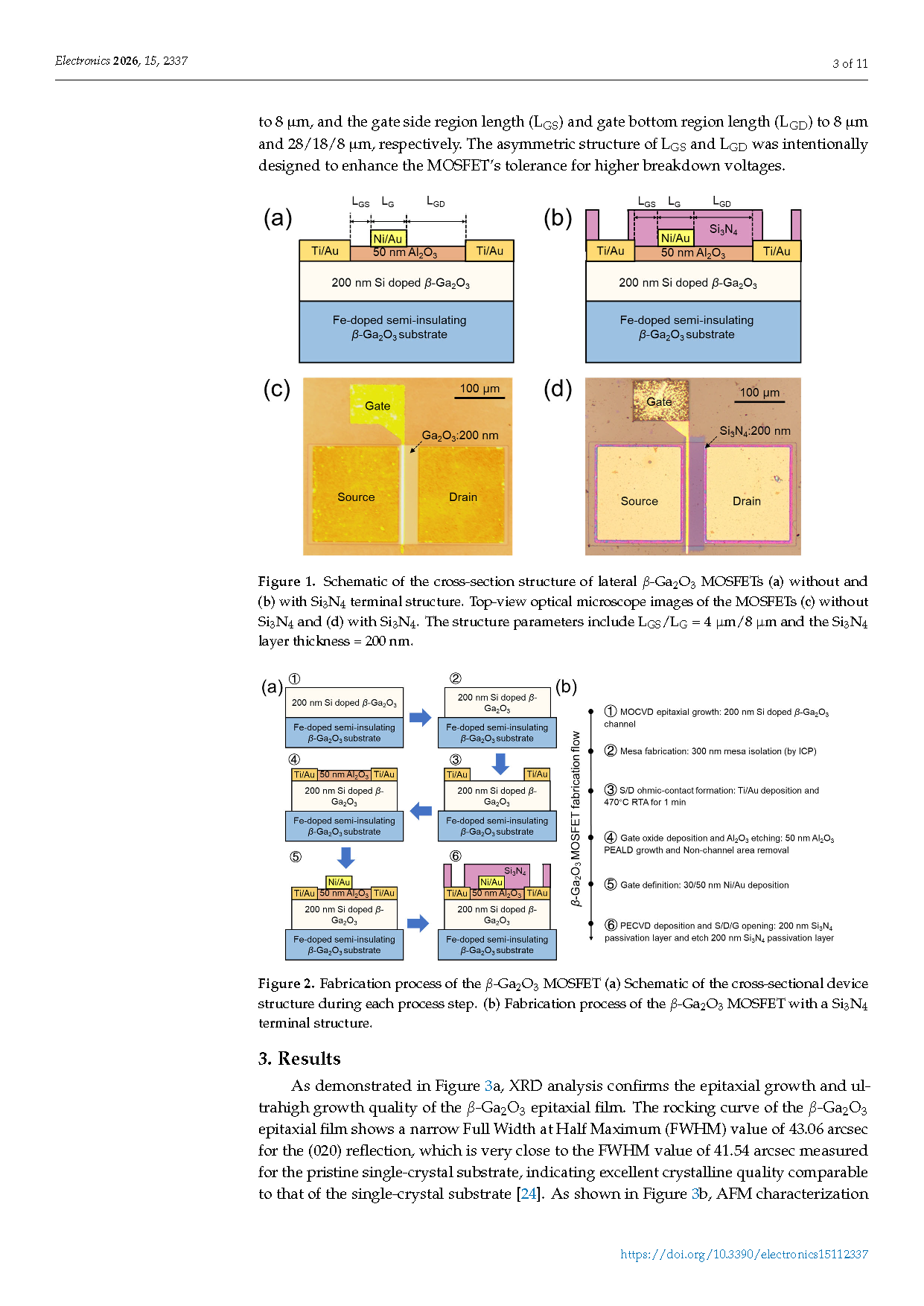
Figure 1 Schematic of the cross-section structure of lateral β-Ga₂O₃ MOSFETs (a) without and (b) with Si₃N₄ terminal structure. Top-view optical microscope images of the MOSFETs (c) without Si₃N₄ and (d) with Si₃N₄. The structure parameters include LGS/LG = 4 μm / 8 μm and the Si₃N₄ layer thickness = 200 nm
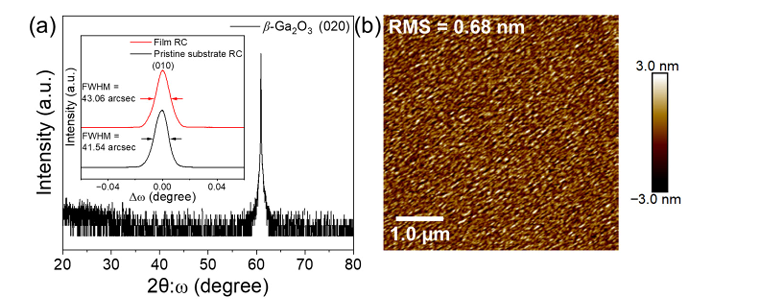
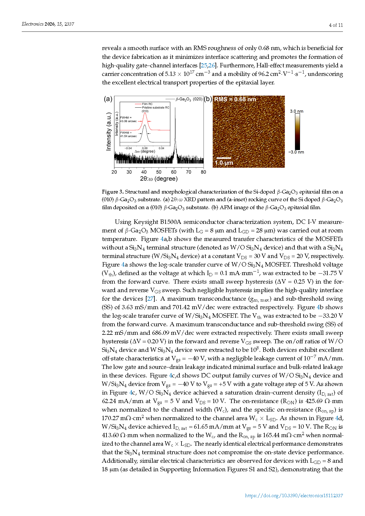
Figure 2 Fabrication process of the β-Ga₂O₃ MOSFET (a) Schematic of the cross-sectional device structure during each process step. (b) Fabrication process of the β-Ga₂O₃ MOSFET with a Si₃N₄ terminal structure.
Figure 3 Structural and morphological characterization of the Si-doped β-Ga₂O₃ epitaxial film on a (010) β-Ga₂O₃ substrate. (a) 2θ:ω XRD pattern and (a-inset) rocking curve of the Si doped β-Ga₂O₃ film deposited on a (010) β-Ga₂O₃ substrate. (b) AFM image of the β-Ga₂O₃ epitaxial film.
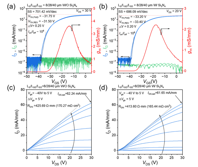
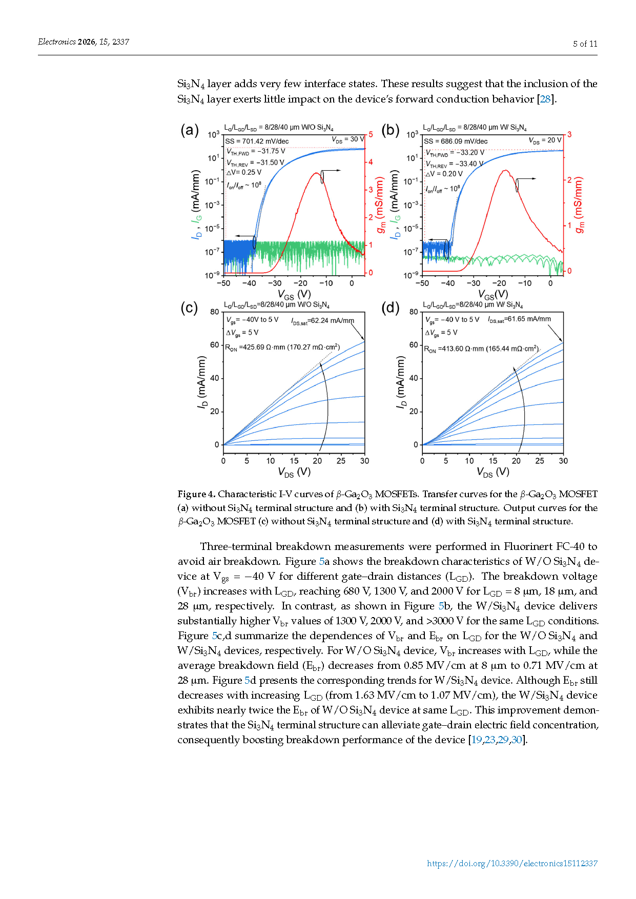
Figure 4 Characteristic I-V curves of β-Ga₂O₃ MOSFETs. Transfer curves for the β-Ga₂O₃ MOSFET (a) without Si₃N₄ terminal structure and (b) with Si₃N₄ terminal structure. Output curves for the β-Ga₂O₃ MOSFET (c) without Si₃N₄ terminal structure and (d) with Si₃N₄ terminal structure.
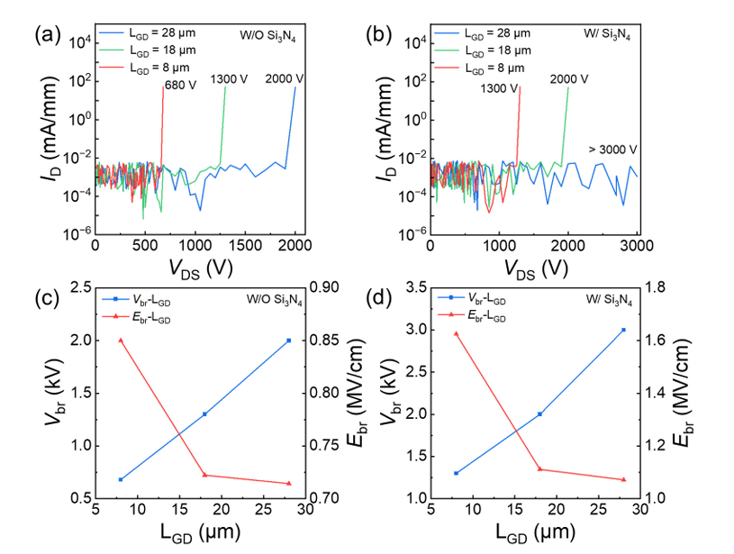
Figure 5 (a) Breakdown curves for the MOSFET without Si₃N₄ terminal structure, with LGD =8 / 18 / 28 μm. (b) Breakdown curves for the MOSFET with Si₃N₄ terminal structure, with LGD =8 / 18 / 28 μm. (c) Relationship between breakdown voltage (Vbr)/average breakdown field strength (Ebr) and LGD for the MOSFET without Si₃N₄ terminal structure. (d) Relationship between Vbr / Ebr and LGD for the MOSFET with Si₃N₄ terminal structure.
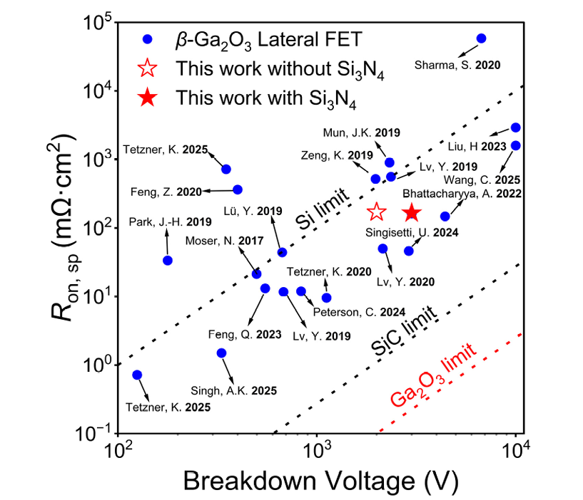
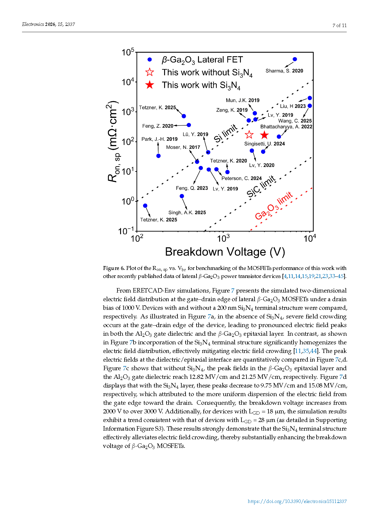
Figure 6 Plot of the Ron,sp vs. Vbr for benchmarking of the MOSFETs performance of this work with other recently published data of lateral β-Ga₂O₃ power transistor devices
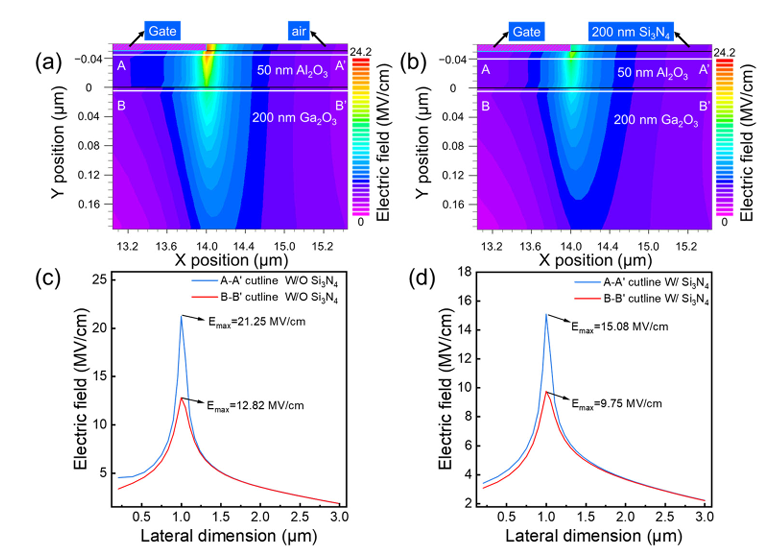
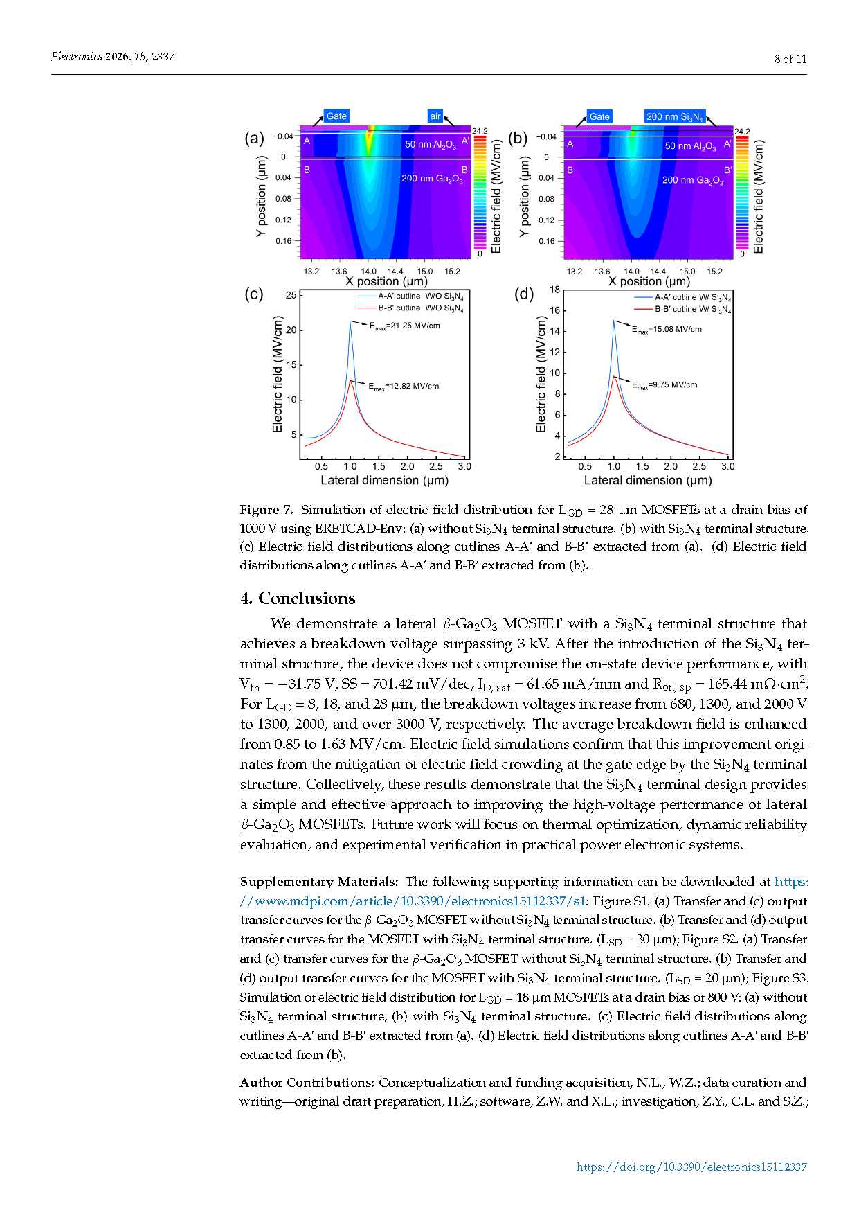
Figure 7 Simulation of electric field distribution for LGD=28 μm MOSFETs at a drain bias of 1000 V using ERETCAD-Env: (a) without Si₃N₄ terminal structure. (b) with Si₃N₄ terminal structure. (c) Electric field distributions along cutlines A-A’ and B-B’ extracted from (a). (d) Electric field distributions along cutlines A-A’ and B-B’ extracted from (b).
DOI:
doi.org/10.3390/electronics15112337

Instruction
Official Account

Cooperation
Top
