


Researchers from the University of Science and Technology of China, Harbin Institute of Technology and Institute of Modern Physics, Chinese Academy of Sciences have published a dissertation titled "Demonstration of β-Ga₂O₃ Lateral Heterojunction Diodes with 450 V Single-event Burnout Voltage" in IEEE Transactions on Nuclear Science.
Background
β-Ga₂O₃, an ultra-wide bandgap semiconductor, is a promising candidate for aerospace electronic systems due to its intrinsic radiation resistance, which enables miniaturization and weight reduction of electronic devices. However, single-event effects (SEE) under space irradiation can generate ion-induced carriers, aggravate electric field crowding, trigger localized overheating, and eventually lead to permanent degradation or catastrophic burnout of power devices.
Conventional vertical β-Ga₂O₃ power diodes suffer poor single-event burnout (SEB) tolerance. Their thick drift epitaxial layers accumulate massive charges under heavy-ion irradiation, drastically reducing reverse breakdown voltage, especially for high-voltage devices. Moreover, the intrinsic material limitations of β-Ga₂O₃ including low hole mobility and poor thermal conductivity further deteriorate the radiation reliability of vertical devices.
The availability of semi-insulating β-Ga₂O₃ substrates and mature epitaxial growth technologies (MOCVD/MBE) support the fabrication of lateral devices with thin epitaxial layers, which can effectively cut down ion-induced charge deposition and improve SEE robustness. In this work, lateral heterojunction diodes (HJDs) integrated with p-type NiO junction termination extension (JTE) are fabricated, and their SEE tolerance is systematically compared with vertical counterparts.
Abstract
This work investigates the single-event effects (SEE) tolerance of lateral β-Ga₂O₃ / NiO heterojunction diodes (HJDs). Under tantalum-ion irradiation with linear energy transfer (LET) of 82.1 MeV·cm²/mg, the lateral HJDs exhibit markedly superior SEE robustness than vertical devices. The ratio of single-event burnout voltage (VSEB) to static breakdown voltage reaches approximately 0.4, substantially surpassing our previously reported vertical HJDs. Meanwhile, the specific ON-resistance of lateral HJDs with an anode-to-cathode length (L_AC) of 10 and 20 μm is calculated to be 13.0 and 36.8 mΩ·cm² respectively, which is comparable to that of vertical diodes. Moreover, the lateral HJDs with L_AC of 20 μm present excellent reliability exposed to heavy-ion irradiation under a reverse bias of 450 V attributed to elongated junction termination extension (JTE) mitigating the surface electric field. This work demonstrates the potential of β-Ga₂O₃ lateral diodes for future radiation-hardened applications.
Highlights
Lateral β-Ga₂O₃HJDs with thin 200 nm drift layer and NiO JTE termination are fabricated for the first time. The ultra-thin drift layer drastically reduces ion-induced charge deposition under heavy-ion irradiation, fundamentally solving the severe SEB issue of vertical devices with thick drift layers.
Heavy-ion irradiation experiments verify that lateral devices own far superior SEB hardness than vertical counterparts. The VSEB/Vbr ratio of lateral HJDs reaches ~0.4, while the maximum ratio of vertical devices is only 0.21. Lateral HJDs with L_AC=20 μm maintain stable electrical performance after irradiation under 450 V reverse bias.
Optical microscopy, EMMI hotspot localization and SEM morphology characterization clarify the lateral SEB failure mode: burnout tracks horizontally extend between anode and cathode, and the anode edge is the core region of electric field crowding and thermal runaway.
A coupled electro-thermal 2D simulation model is established to reveal the physical SEB mechanism: ion-generated holes accumulate at the anode edge and trigger severe electric field crowding and impact ionization, forming a positive feedback thermal runaway loop. Increasing L_AC and extending JTE can suppress peak surface electric field and lattice temperature, thus improving radiation tolerance.
Lateral HJDs achieve comparable on-state performance with vertical diodes while delivering outstanding radiation hardness, providing a novel structural route for radiation-hardened wide-bandgap power electronics used in aerospace.
Conclusion
In summary, this work investigates the SEE hardness of β-Ga₂O₃ lateral HJDs. Benefiting from the low charge deposition within the thin epitaxial layer and the effective surface electric field reduction with JTE structure, the lateral HJDs with LAC of 10 and 20 μm achieved VSEB of 350 V and exceeding 450 V, respectively. Burnout morphology analysis and SEE simulations demonstrate that ion-induced hole accumulation at the anode edge drives electric field crowding and localized overheating, triggering thermal runaway till catastrophic failure. These results demonstrate the superior radiation hardness of the β-Ga₂O₃ lateral diodes and offer strategic guidance for surface electric field modulation to further enhance SEE resilience.
Project Support
This work is supported by the National Natural Science Foundation of China under Grant nos. U23A20358, 62522411, 62474170, 62404214, 62234007 and 62474170, the National Key Research and Development Program of China (No. 2024YFE0205200), Provincial Science and Technology Major Project of Jiangsu under Grant No. BG2024030, the open research fund of Suzhou Laboratory under Grant no. SZLAB-1208-2024-ZD012.
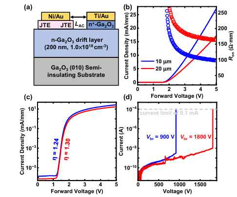
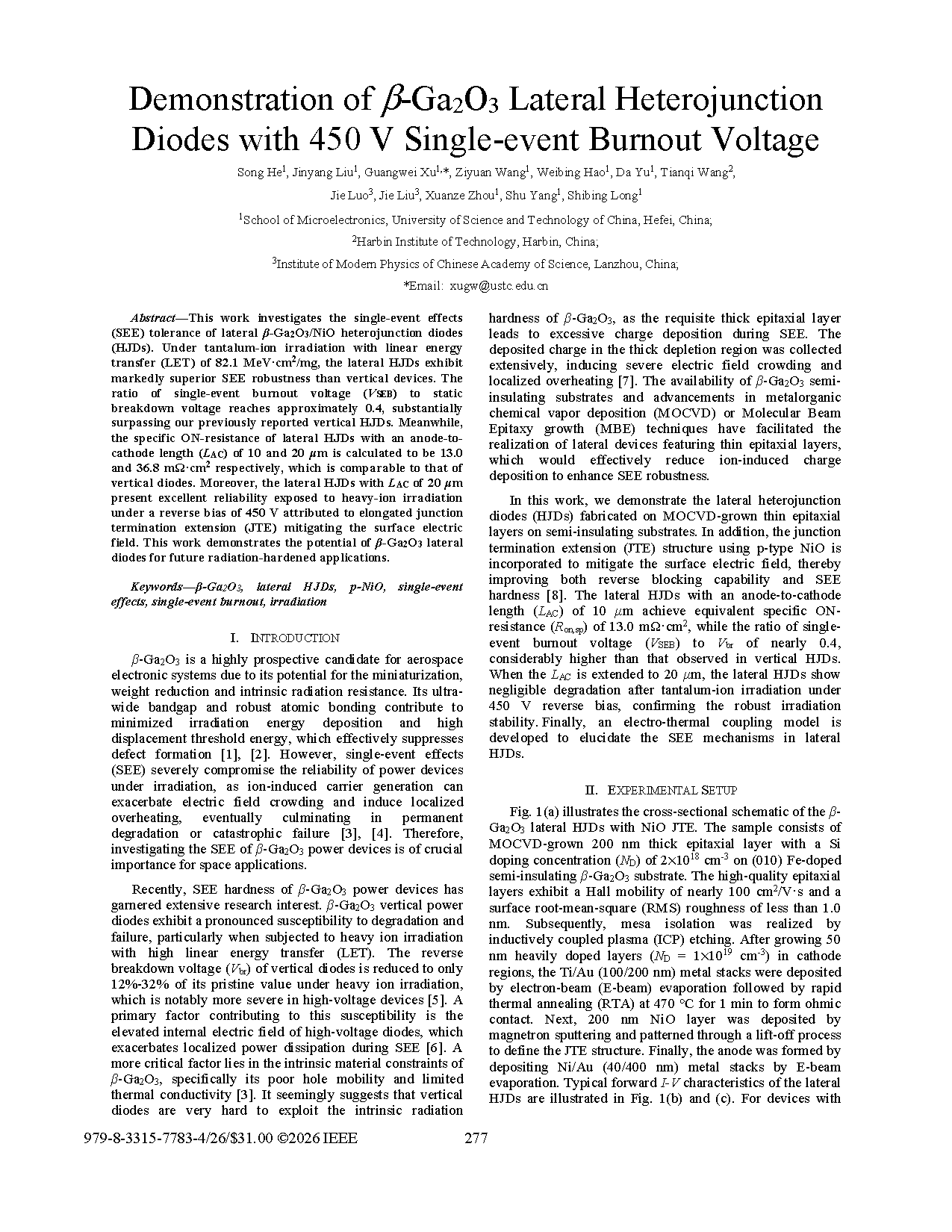
Figure 1 (a) Cross-section schematic, forward I-V characteristics in (b) linear and (c) log-scale and (d) Vbr of lateral HJDs with JTE.
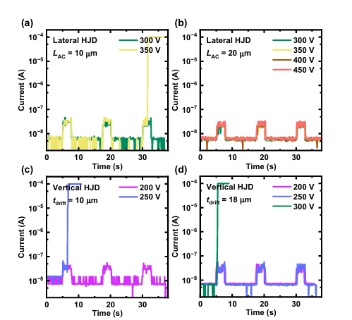
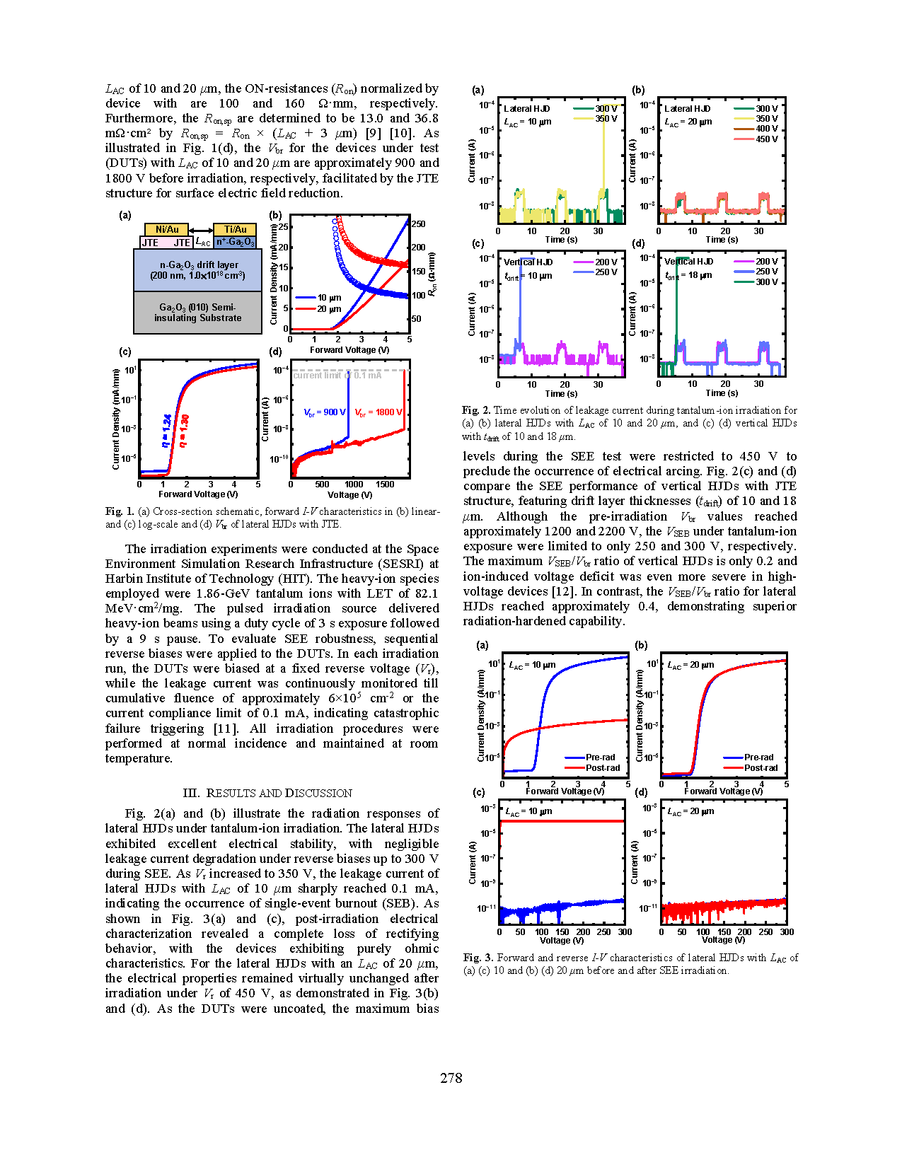
Figure 2 Time evolution of leakage current during tantalum-ion irradiation for (a) (b) lateral HJDs with LAC of 10 and 20 μm, and (c) (d) vertical HJDs with tdrift of 10 and 18 μm.
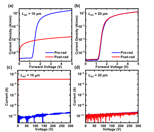
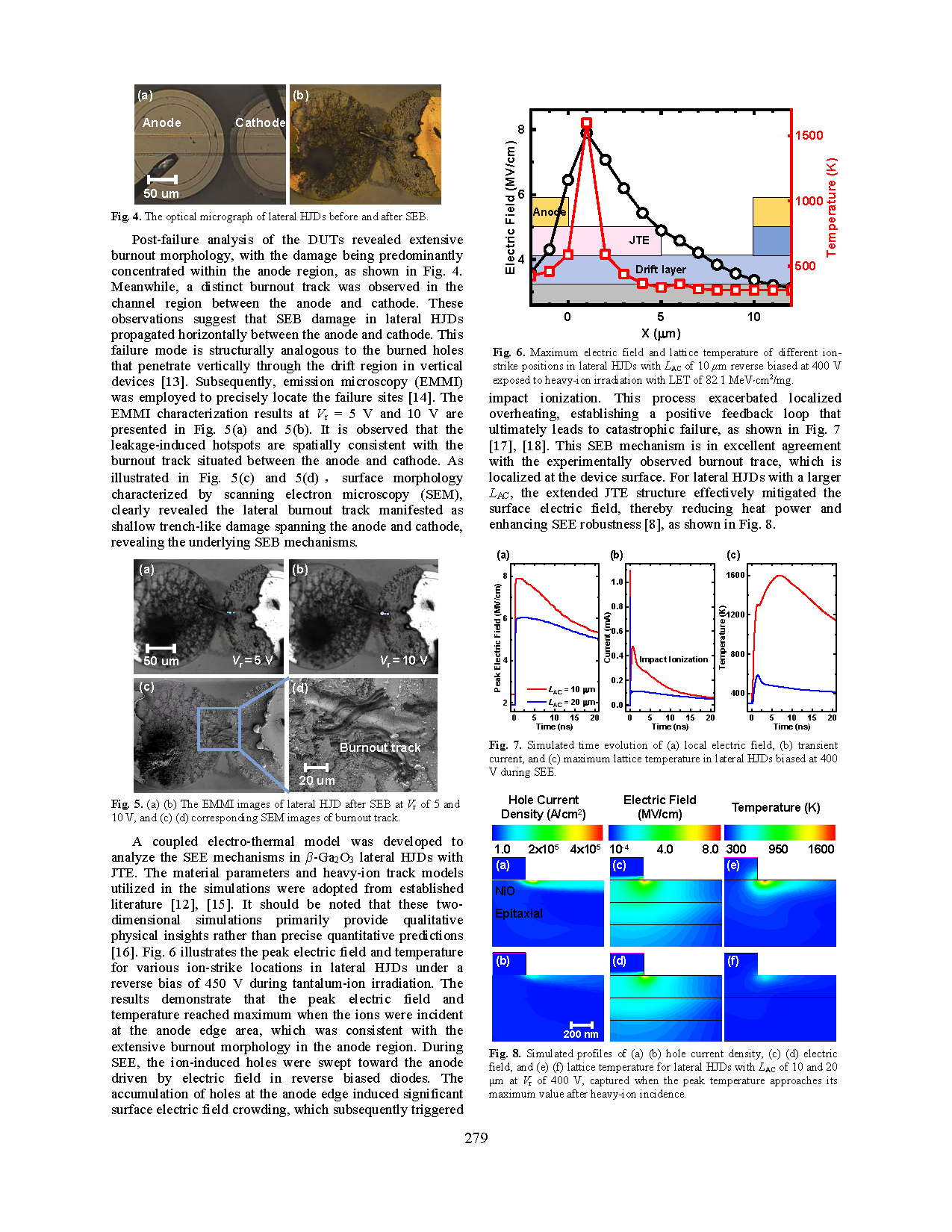
Figure 3 Forward and reverse I-V characteristics of lateral HJDs with LAC of (a) (c) 10 and (b) (d) 20 μm before and after SEE irradiation.
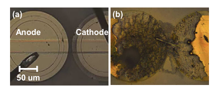
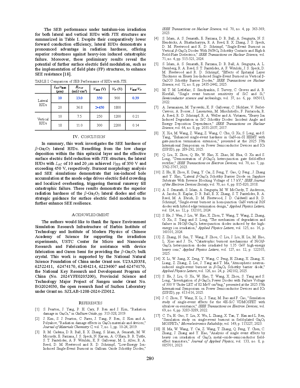
Figure 4 The optical micrograph of lateral HJDs before and after SEB.
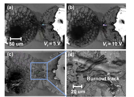
Figure 5 (a) (b) The EMMI images of lateral HJD after SEB at Vr of 5 and 10 V, and (c) (d) corresponding SEM images of burnout track.
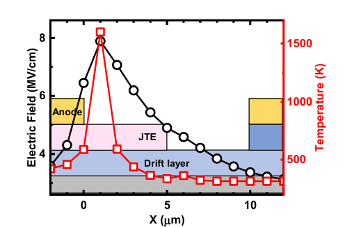
Figure 6 Maximum electric field and lattice temperature of different ion-strike positions in lateral HJDs with LAC of 10 μm reverse biased at 400 V exposed to heavy-ion irradiation with LET of 82.1 MeV・cm²/mg
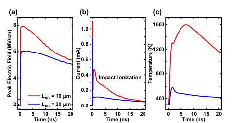
Figure 7 Simulated time evolution of (a) local electric field, (b) transient current, and (c) maximum lattice temperature in lateral HJDs biased at 400 V during SEE.
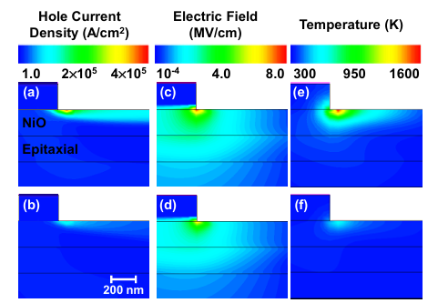
Figure 8 Simulated profiles of (a) (b) hole current density, (c) (d) electric field, and (e) (f) lattice temperature for lateral HJDs with LAC of 10 and 20 μm at Vr of 400 V, captured when the peak temperature approaches its maximum value after heavy-ion incidence.
DOI:
10.1109/ISPSD64561.2026.11553930
Instruction
Official Account

Cooperation
Top
